This project is an open source (MIT license) MIPI CSI-2 receive core for Xilinx FPGAs, supporting 4k resolution at greater than 30fps. It includes a complete demo project, designed for the Genesys 2 board with a custom FMC to camera card, that writes the 4k video into a DDR3 framebuffer and outputs at 1080p (with a choice of scaled or cropped) to the HDMI and VGA ports. The demo camera module is the Omnivision OV13850 (using the Firefly camera module), which supports 4k at up to 30fps, although the demo runs at 24fps where it seems performance is better - this may partly be down to the choice of register values though. Although the OV13850 sensor/ADC does not seem to work much above 30fps; the camera also has a "test pattern" mode which bypasses this and which I have used to test my driver up to 45fps.
- The
mipi-csi-rxfolder contains all the components (except thevideo_timing_ctrltiming generator, in thevideo-miscfolder) needed for the CSI-2 Rx itself.csi_rx_topis the top level for the CSI-2 interface, this is what you should use in your designcsi_rx_4_lane_linkencapsulates the link layer. In particularcsi_rx_hs_lane_phyis the low-level data PHY, one for each lane, containing the input buffer and input SERDEScsi_rx_byte_alignensures bytes are correctly aligned by looking for the sync byte that precedes packetscsi_rx_word_aligncorrects any slight alignment differences between lanes, concatenating the 4 lane byte inputs to a single 32-bit word outputcsi_rx_hs_clk_phyhandles the clock input and contains the necessary clock buffers
csi_rx_packet_handlerprocesses packets, looking for video packets and seperating off the payloadcsi_rx_10bit_unpackconverts 32-bit packet payload input and outputs 4 10-bit pixels (with avalidoutput, as it does not produce pixels every clock cycle)csi_rx_video_outputsynchronises the CSI-2 clock domain to the pixel clock domain using a line buffer and outputs standard video format
ov-cam-controlcontains a I2C interface for camera configuration, the 4k24 configuration for the OV13850, andov13850_control_topwhich handles camera reseting and writes the register values from the configuration ROM to the I2C interface.framebuffer-ctrlcontains the framebuffer controller, which interfaces with external framebuffer memory (providing an AXI4 master to interface with the Xilinx DDR3 controller) to scale or crop the 4k frames from the camera to 1080p for the video output.video-misccontains the video timing controller, a test pattern generator for debugging, a video register for timing purposes and the basic ISP (a simple debayering core and colour channel gain adjustment for white balance).dvi-txcontains a simple DVI transmitter, for the Genesys 2 HDMI output portdemo-topcontains the top level files for the demo project; andexamplescontains the Vivado project itself for the demo
The current test platform is the Digilent Genesys 2 (Kintex-7 XC7K325T-2) with an OV13850 camera. The CSI-2 lanes connect to 2.5V LVDS inputs on the FPGA, using a custom FMC interface board. Earlier testing was done on a Virtex-6 FPGA, unfortunately I no longer have access to this platform so support cannot be guaranteed.
The exact camera used was the Firefly RK3288 camera module, which is a convenient way of obtaining the OV13850 camera - search for "OV13850 Firefly RK3288" and various sites selling it can be found starting from $40 or so. In the future I'm looking into using smartphone replacement camera modules. I have ordered some IUNI U2 replacement back cameras which are P16V01A modules based on the 4k60-capable OV16825 and have a publicly available pinout.
The first version of my FMC breakout board, which I am using at the moment, has some serious flaws and has required various bodges so I am not releasing the design for this version. I have ordered a new version and will post the designs for this once I receive it if it works. The board also has a connector for the 4k 5.5" Z5 premium LCD; which I am also working on code to drive.
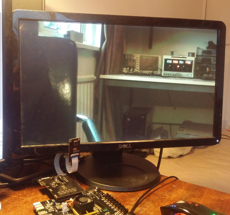
A quick picture of my test setup is below.
See csi_rx_top.vhd for more information on the parameters that need to be adjusted depending on your camera and application.
In the future the debayering block needs to be improved to reduce colour fringing at sharp edges. A driver for the focus voice coil driver inside the camera module needs to be added; along with autofocus and AEC/AGC (at the moment gain and exposure are buried deep within the camera config ROM).
