pPropQL020
An extended version of pPropQL. As MC68008 are scarce and I have some, plenty, MC68EC020s I decided to improve pPropQL with a more powerful processor, more memory, programmable logic and loads of fun.
The glue logic of pPropQL has been incorporated into three small CPLDs, they could be replaced by a bigger, and I mean with more IOs, CPLD. The rationale behind the CPLDs is: this board can be re-targeted. The memory map of the QL is just not that nice to run for instance OMU.
The two I/O Propellers have been kept but now the control over the address mux is handled by the memory-decoding logic and a wait-state generator, as well as the generation of the DSACK0/1 (bus termination signals), freeing powerful propeller pins.
The EPROM that existed in the pPropQL has been left out, so booting and loading a kernel image is the task of a boot-loader inside the video Propeller. This bootloader reads the the image from a SD/MMC card, copies it to memory and executes it.
Note: assert and negate are used to specify forcing a signal to a particular state. In particular, assertion and assert refer to a signal that is active or true; negation and negate indicate a signal that is inactive or false. These terms are used independently of the voltage level (high or low) that they represent. Note: Signals are in bold. A signal's name starting with an N means that that signal is active low, assertion will mean a logic 0 level in positive logic (used here). Only one of the three will preferably used here.
A discussion of this board can be found here.
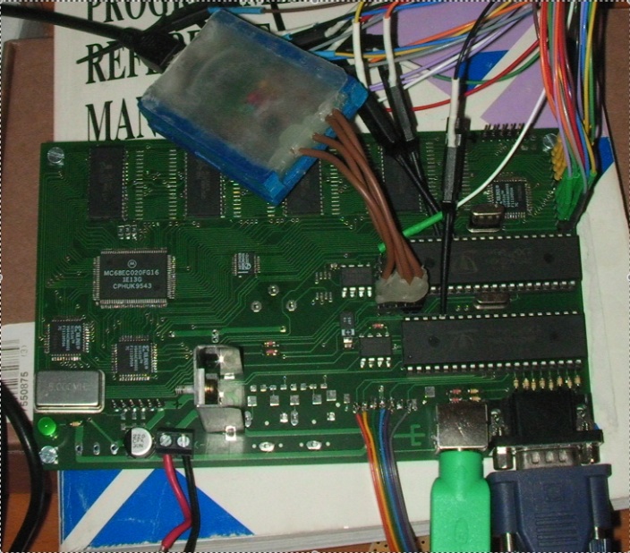
The MC68EC020 processor is a 5V part thus some level shifting is needed between the propeller and the 68K. The address bus mux, inside the third CPLD, acts as a level shifter. Its core voltage is kept at 5V while its IO voltage is 3.3V. This part is a XC9536. The data bus is buffered via a 74ABT245 and connected to the propeller using current-limiting resistors. Control lines use also current-limiting resistors.
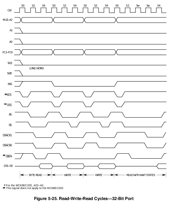
All glue logic has been implemented using XC9536s (CPLD). Memory decoding is handled by U11 and the glue is by U10. The Glue logic has to generate the byte strobe signals for memory and several other signals like NHALT, NRESET, NOE usw. The 020 uses two Data Acknowledge signals to signal the end of the bus cycle and thus to determine the port size. The port sizes used are 32 bits for SRAM and 8 bits for the propellers. At the beginning of a cycle the signals A1, A0, SIZ0 and SIZ1 say what kind of transfer size is being performed and to which address. Decoding of those signals yields the byte strobes for writing (NWE0 to NWE3). In a 32 bit port, like the SRAM here, all byte strobes are used.
| Byte strobe | bits used | Equations |
|---|---|---|
| NWE3 | D7..D0 | !(!A0 & !A1 & !RW & !NDS) |
| NWE2 | D16..D8 | !((SIZ1 & !A1 & !RW & !NDS) |
| NWE1 | D23..D16 | !((!A0 & A1 & !RW & !NDS) |
| NWE0 | D31..D24 | !((SIZ1 & A1 & !RW & !NDS) |
The QL uses only IPL2 as interrupt input and asserts the NVMA input in the MC68008 for autovector interrupts. On the MC68020 this NVMA signal does not exist but an NAVEC input for auto-vector interrupt recognition is provided. This signal is asserted when the function code outputs (FC2 to FC0) signal an interrupt acknowledge cycle.
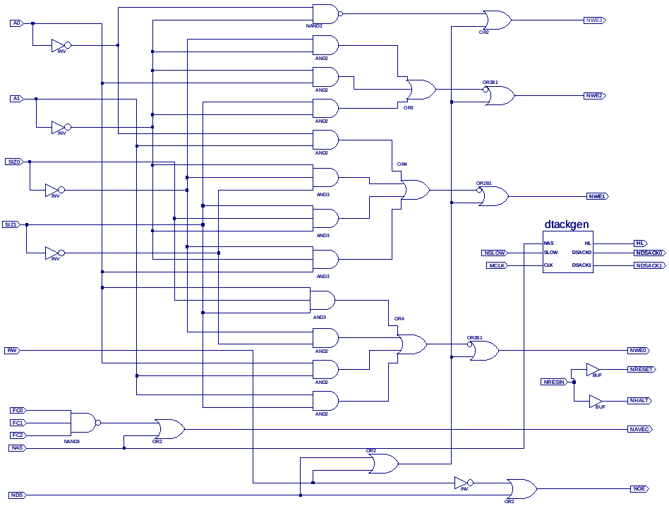
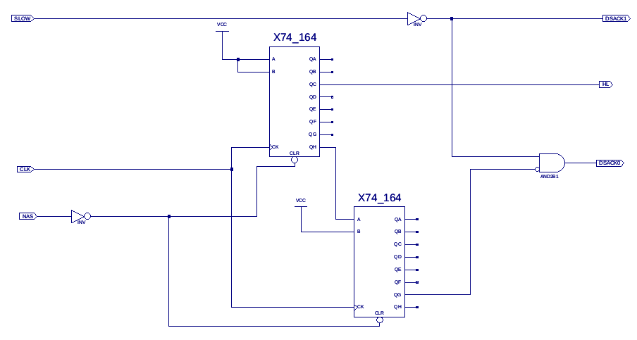
The DSACK generator for DSACK0..1 uses a pair of cascaded shift registers. HL is asserted three cycles after NAS when NSLOW is also asserted and thus the BUS cycle is not terminated by a 32-bit port access (i.e. both DSACK0 and DSACK1 are asserted before S4). This signal handles the address mux, contained in U14. After one of the IO strobes is asserted at least 50 ns pass before the propeller reads the low address byte so 3 wait states are needed as a minimum. After this read there is place for 2 or 3 more propeller instructions before the high address byte can be read. As the low address byte has to be masked and shifted this does not pose a problem. (See the logic analyzer's traces below).
Memory decoding is done with simple 3-to-8 decoders and some gates
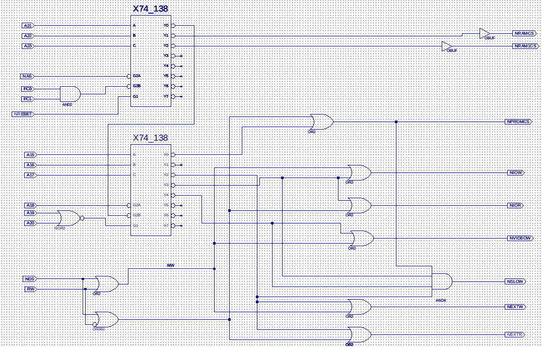
The memory map used here is similar to the QL's except for the fact that the SRAM is mapped to the addresses 0x20_0000 to 0x5F_FFFF, 4 MBytes.
As I'm not really interested in using this for QL and more in porting OMU to it, this memory configuration maximizes available memory.
Video memory is as the built prototypes only writable but that can be changed to read/write with a simple piece of wire and a change to U11 to make VIDEOR available.
A Verilog implementation of the above circuits, both condensed into one CPLD could be this one. EIOR and EIOW are not implemented due to the lack of pins in the XC9536 used. A XC9572 could be used instead, then the Address/Data MUX could be fitted inside too.
`timescale 1ns / 1ps
//////////////////////////////////////////////////////////////////////////////////
// Company:
// Engineer: Pacito.Sys
//
// Create Date:    09:04:29 01/21/2010
// Design Name: pPropQL020 glue logic
// Module Name:    gluelogic
// Project Name: pPropQL020
// Target Devices: XC9536
// Tool versions: Xilinx WebISE 10.1
// Description: Glue logic for the pPropQL
//
// Dependencies:
//
// Revision:
// Revision 0.02 - Simulated
// Additional Comments:
//
//////////////////////////////////////////////////////////////////////////////////
module gluelogic(
    input in_clk,
    input in_fc0,
    input in_fc1,
    input in_nas,
    input in_nds,
	 input in_rw,
	 input in_siz0,
	 input in_siz1,
	 input A0,
	 input A1,
    input A15,
    input A16,
    input A17,
    input A18,
    input A19,
	 input A20,
	 input A21,
	 input A22,
	 input A23,
	 output AVEC,
    output NDSACK0,
	 output NDSACK1,
    output HL,
    output IOR,
    output IOW,
    output VIDEOW,
    output NROMCS,
    output NRAMCS0,
	 output NRAMCS1,
	 output NOE,
	 output WE3,
	 output WE2,
	 output WE1,
	 output WE0//,
	 //output EIOR,
	 //output EIOW
    );

reg [3:0] r_dtackshift; // wait state counter
/* pPropQL Memory Map
 *
 * 000000..00FFFF RW NROMCS
 * 010000..017FFF R  EIOR (with wait states)
 * 010000..017FFF W  EIOW (with wait states)
 * 018000..01FFFF R  IOR (with wait states)
 * 018000..01FFFF W  IOW (with wait states)
 * 020000..027FFF W  VIDEOW, NRAMCS0 (with wait states)
 * 020000..027FFF R  NRAMCS0
 * 1FFFFF..1FFFFF RW NRAMCS0
 * 200000..3FFFFF RW NRAMCS1
 */
// Internal signals
wire int_r = ~(in_nas | ~(in_fc0 & in_fc1)) | ~in_rw | in_nds;
wire int_w = ~(in_nas | ~(in_fc0 & in_fc1)) | in_rw | in_nds;
wire int_00 = A23 | A22 | A21 | A20;
wire int_romcs = int_00 | A19 | A18 | A17 | A16;
wire int_extra = int_00 | A19 | A18 | A17 | ~A16 | A15;
wire int_io = int_00 | A19 | A18 | A17 | ~A16 | ~A15;
wire int_video = int_00 | A19 | A18 | ~A17 | A16 | A15;
wire int_nramcs0 = A23 | A22 | A21 | ~int_romcs | ~int_io | ~int_extra;
wire int_nramcs1 = A23 | A22 | ~A21;

// ** Outputs **
assign AVEC = in_nas | ~(in_fc0 & in_fc1);
// Chip selects
assign NROMCS = int_romcs | int_r;
assign NRAMCS0 = int_nramcs0 | in_nds;
assign NRAMCS1 = int_nramcs1 | in_nds;
assign VIDEOW = int_video | int_w;
//assign EIOR = int_r | int_extra;
//assign EIOW = int_w | int_extra;
assign IOR = int_r | int_io;
assign IOW = int_w | int_io;

// Extra outputs
assign NOE = int_r;
assign WE3 = ~(~A0 & ~A1 & ~in_rw & ~in_nds);
assign WE2 = ~( (in_siz1 & ~A1 & ~in_rw & ~in_nds) |
                (~in_siz0 & ~A1 & ~in_rw & ~in_nds) |
					 (A0 & ~A1 & ~in_rw & ~in_nds) );
assign WE1 = ~( (~A0 & A1 & ~in_rw & ~in_nds) |
					 (in_siz0 & in_siz1 & ~A1 & ~in_rw & ~in_nds) |
					 (~in_siz1 & ~in_siz0 & ~A1 & ~in_rw & ~in_nds) |
					 (~in_siz0 & A0 & ~in_rw & ~in_nds) );
assign WE0 = ~( (in_siz1 & A1 & ~in_rw & ~in_nds) |
					 (~in_siz1 & ~in_siz0 & ~in_rw & ~in_nds) |
					 (A0 & A1 & ~in_rw & ~in_nds) |
					 (in_siz1 & in_siz0 & A0 & ~in_rw & ~in_nds) );

// DTACK generation

wire int_slow = VIDEOW & IOR & IOW;
assign NDSACK0 = (r_dtackshift < 14) & ~int_slow;
assign NDSACK1 = int_slow;

// High, low signal
assign HL = r_dtackshift > 1;
always @(posedge in_clk)
begin
	if (in_nas)
		r_dtackshift <= 0;
	else
		if (~int_slow) begin
			r_dtackshift <= r_dtackshift + 1;
		end
end

initial
begin
	r_dtackshift = 0;
end
endmodule
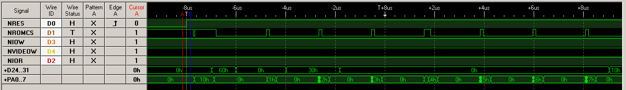
Two propellers are used as video controller one and IO controller the other one. They are memory mapped and thus act as any other memory. This propellers present a simple interface, data bus (D24..31) address bus (multiplexed A0 to A15) and one strobe signal per function, read, write and so on.
Upon assertion of the strobe signal the propeller decodes the address and performs whatever action is needed. All this processing has to take place in the allocated time, 15 or 16 MC68K cycles. 1 us @ 16 MHz or 2 us @ 8 MHz (used now for testing).
The following logic analyzers' trace show the state of various signals when NIOR is asserted. PA0..7 are the multiplexed addresses and D24..31 are the lowest significant bits of the data bus used for 8 bit transfers.
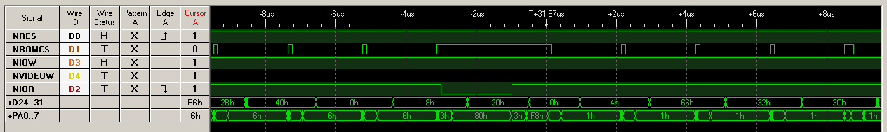
The assertion of NVIDEOW proceeds in a similar manner.
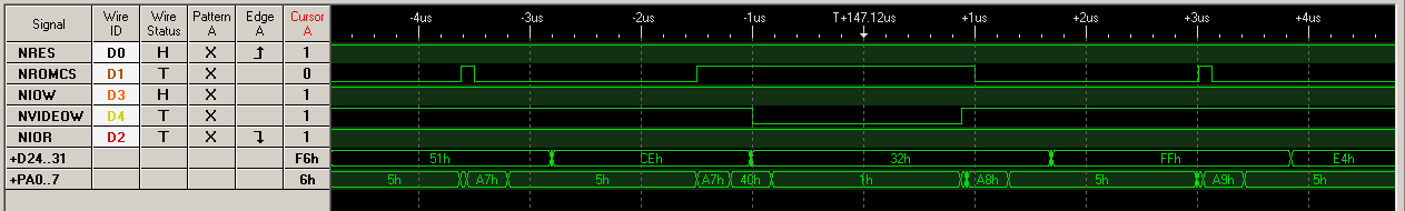
As can be seen the data bus changes state some 700 to 800 ns after the assertion of NIOR/NVIDEOW. As the data is latched on the rising edge of NDS (or'd to NIOx/NVIDEO) there is enough time. All this examples were done @ 8 MHz.
The answering code for this could be something like this:
DAT
                        org     $0

VIDEOCOG                mov     DIRA, #0

c2_videoemu             waitpne c2_c_VIDEOW, c2_c_VIDEOW ' waits for VIDEOW to be asserted

                        mov     c2_v_addr, INA          '@ 40   gets low part of address
                        shr     c2_v_addr, #16          '@ 80
                        and     c2_v_addr, #255         '@120
                        add     c2_v_addr, PAR          '@160 adds video buffer offset
#ifdef M68K_8MHz
                        nop                             ' this NOPs ensure that the high address
                        nop                             ' is available to be read
                        nop
#endif
                        mov     c2_v_addrh, INA         '@320 now it is safe to get high addr
                        mov     c2_v_data, c2_v_addrh
                        shr     c2_v_addrh, #8          '@360
                        and     c2_v_addrh, c2_c_MSKADDR
                        add     c2_v_addr, c2_v_addrh   '@400
                        wrbyte  c2_v_data, c2_v_addr    '@440
                                                        '@715 (max)
                        waitpeq c2_c_VIDEOW, c2_c_VIDEOW ' waits for NVIDEOW to be negated
                        jmp     #c2_videoemu


c2_c_VIDEOW             long    1<<VIDEOW
c2_v_addr               long    0
c2_v_addrh              long    0
c2_v_data               long    0
c2_c_MSKADDR            long    $00000f00   ' only 4 kbytes !!!!
The reset is handled by one COG and one PIN as output. As the video propeller acts as boot ROM, it answers the NPROMCS signal. After reset the stack pointer and the reset vector are fetched and execution starts at that address (0x0000_0010 in this case).
The following code fragment shows the (wasted) cog. Any COG would do in principle, so it can be devoted to something else afterwards.
DAT
                        org     $0

RESETCOG                mov     OUTA, #0
                        mov     DIRA, c1_c_DIRA

                        or      OUTA, c1_c_RESET        ' negates NRESET and NHALT
                        mov     c1_v_wait, CNT
                        add     c1_v_wait, c1_c_80M
c1_loop                 waitcnt c1_v_wait, c1_c_80M
                        jmp     #c1_loop

c1_c_DIRA               long    1<<RESET           ' RESET
c1_c_RESET              long    1<<RESET
c1_v_wait               long    0
c1_c_80M                long    80_000_000