DMASupportToReceiveTransmitPacket
The DMA support in the NetFPGA hardware to receive/transmit packets includes a DMA master in the CPCI chip and a DMA slave in the NetFPGA chip. There is a dedicated DMA interface of pins between the CPCI chip and the NetFPGA chip for two operation modes: CPU RX queue packet availability and TX queue full status in the NetFPGA chip, and packet transfer from the CPU RX queue in the NetFPGA chip to the CPCI chip. The other operation mode, packet transfer from the CPCI chip to the CPU TX queue in the NetFPGA chip, uses the pins of the CPCI chip and the NetFPGA chip, which conduct the normal NetFPGA chip register read/write operations.
In this article the focus is on the NetFPGA chip part, because a typical NetFPGA user needs to instantiate the DMA module and connect the CPU RX/TX queues to the DMA module in the NetFPA chip. The CPCI chip design needs no change for a typical NetFPGA user to implement his specific design.
- In the NetFPGA chip the DMA slave module is named nf2_dma with three submodules: nf2_dma_bus_fsm, nf2_dma_sync and nf2_dma_que_intfc. Their interaction with the NetFPGA chip pins and the CPU RX/TX queues is shown in this diagram.

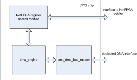
- In the CPCI chip the DMA master includes the following modules: dma_engine, cnet_dma_bus_master. Their block level diagram is shown in this figure.
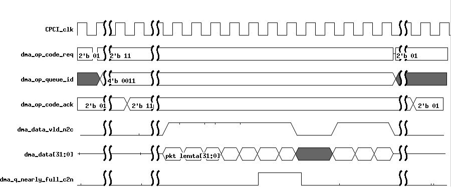
- The dedicated DMA interface between the CPCI chip and the NetFPGA chip has the following signals.
| Signal Group | Signal Name | Direction | Bits | Description |
| Operation Code Negotiation | dma_op_code_req | from CPCI chip to NetFPGA chip | 2 | CPCI requests NetFPGA to perform one of the following operations. 2'b 01: report CPU RX queue packet availability and CPU TX queue full status. 2'b 10: data transfer from CPCI to NetFPGA (to be supported by the CPCI chip). 2'b 11: data transfer from NetFPGA to CPCI. |
| Operation Code Negotiation | dma_op_queue_id | from CPCI chip to NetFPGA chip | 4 | Specifies which CPU queue to transfer from/to. 4'h F is CPU queue 15, 4'h 0 is CPU queue 0 and so on. |
| Operation Code Negotiation | dma_op_code_ack | from NetFPGA chip to CPCI chip | 2 | Acknowledges that the NetFPGA chip has received the dma_op_code_req from the CPCI chip. |
| DMA_RX | dma_data_vld_n2c | from NetFPGA chip to CPCI chip | 1 | Specifies if the dma_data is valid. |
| DMA_RX | dma_data | bi-directional | 32 | The NetFPGA chip drives the packet length in its first valid cycle and the packet data in the subsequent valid cycles on this bus. |
| DMA_RX | dma_dest_q_nearly_full_c2n | from CPCI chip to NetFPGA chip | 1 | This signal is 1 if the CPCI chip wants to pause the packet data transfer from the NetFPGA chip to the CPCI chip. Otherwise this signal is 0. |
| DMA_TX (future work in CPCI chip) | dma_data_vld_c2n | from CPCI chip to NetFPGA chip | 1 | Specifies if the dma_data is valid. |
| DMA_TX (future work in CPCI chip) | dma_data | bi-directional | 32 | The CPCI drives the packet length in its first valid cycle and the packet data in the subsequent valid cycles on this bus. |
| DMA_TX (future work in CPCI chip) | dma_dest_q_nearly_full_n2c | from NetFPGA chip to CPCI chip | 1 | This signal is 1 if the NetFPGA chip has its CPU TX queue nearly full and wants to pause the packet data transfer from the CPCI chip to the NetFPGA chip. Otherwise this signal is 0. |
- Packet data transfer from the CPCI chip to the NetFPGA chip uses the following register access signals.
| Signal Name | Direction | Bits | Description |
| cpci_req | from CPCI chip to NetFPGA chip | 1 | Be asserted for one clock cycle for every 32-bit packet data transfer. |
| cpu_rd_wr_L | from CPCI chip to NetFPGA chip | 1 | Be deasserted because the packet data transfer is done by NetFPGA register write. |
| cpci_addr | from CPCI chip to NetFPGA chip | 27 | This signal encodes the address of the CPU TX queue write interface register. |
| cpci_data | from CPCI chip to NetFPGA chip | 32 | This signal encodes the packet data transferred from the CPCI chip to the NetFPGA chip. |
| cpci_wr_rdy | from NetFPGA chip to CPCI chip | 1 | This signal is asserted when the NetGPA chip is ready to accept a register write request. |
- The interface between the nf2_dma module and the CPU RX/TX queues in the NetFPGA chip has the following signals.
| Signal Group | Signal Name | Direction | Bits | Description |
| Interface to CPU RX queue | cpu_q_dma_rd | from nf2_dma module to CPU RX queue | 1 | When asserted 32-bit packet data are read out from the CPU RX queue. |
| Interface to CPU RX queue | cpu_q_dma_rd_data | from CPU RX queue to nf2_dma module | 32 | the packet data read out from the CPU RX queue |
| Interface to CPU RX queue | cpu_q_dma_rd_ctrl | from CPU RX queue to nf2_dma module | 4 | the packet EOP information read out from the CPU RX queue |
| Interface to CPU TX queue | cpu_q_dma_wr | from nf2_dma module to CPU TX queue | 1 | When asserted 32-bit packet data are written to the CPU TX queue. |
| Interface to CPU TX queue | cpu_q_dma_wr_data | from nf2_dma module to CPU TX queue | 32 | the packet data written to the CPU TX queue |
| Interface to CPU TX queue | cpu_q_dma_wr_ctrl | from nf2_dma module to CPU TX queue | 4 | the packet EOP information written to the CPU TX queue |
The DMA slave module in the NetFPGA chip supports three operation modes: CPU RX queue packet availability and TX queue full status report mode (aka CPU queue status mode), transfer from the NetFPGA chip to the CPCI chip mode (aka DMA-RX mode), transfer from the CPCI chip to the NetFPGA chip mode (aka DMA-TX mode).
- CPU queue status mode

- DMA-RX mode
- DMA-TX mode

The DMA transfer data throughput information is as follows.
- DMA-RX operation mode:
- Transfer from a CPU RX queue to the store-and-forward FIFO in the nf2_dma_bus_fsm module of the NetFPGA chip has data throughput 4 bytes per 62.5 MHz clock cycle, i.e. 2 Gbps.
- Transfer from the store-and-forward FIFO in the nf2_dma_bus_fsm module of the NetFPGA chip to the store-and-forward FIFO in the cnet_dma_bus_master module of the CPCI chip has data throughput 4 bytes per 62.5 MHz clock cycle, i.e. 2 Gbps.
- Transfer from the store-and-forward FIFO in the cnet_dma_bus_master module of the CPCI chip to the memory location on the host computer has data throughput 4 bytes per 33.3 MHz clock cycle, i.e. 1.06 Gbps.
- DMA-TX operation mode:
- Transfer from the memory location on the host computer to an asynchronous cut-through FIFO in the CPCI chip has data throughput 4 bytes per 33.3 MHz clock cycle, i.e. 1.06 Gbps.
- Transfer from the asynchronous cut-through FIFO in the CPCI chip to the CPU TX queue in the NetFPGA chip has data throughput 4 bytes every 3 cycles in 125 MHz clock domain, i.e. 1.33 Gbps.