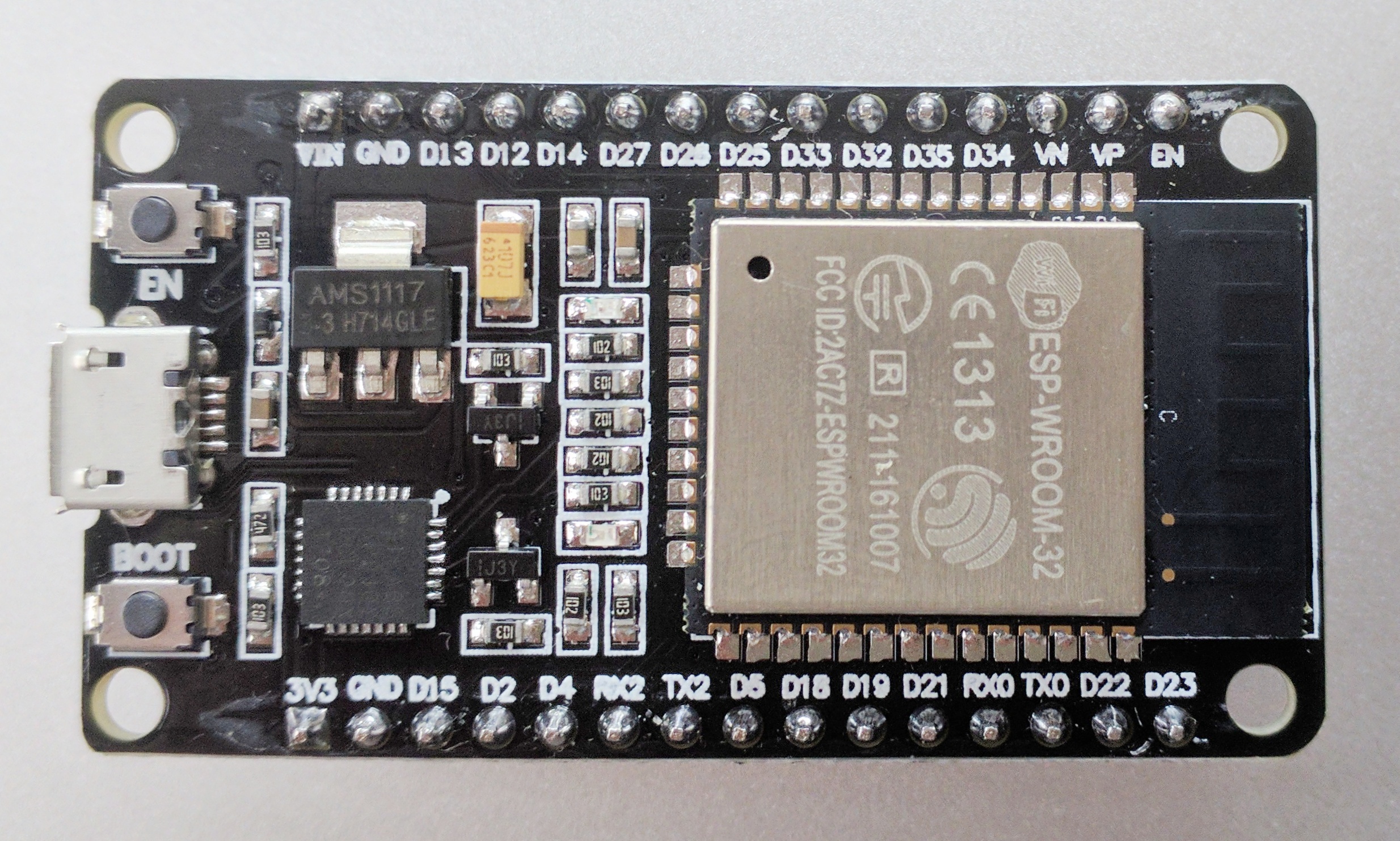
Skip to content
New issue

Have a question about this project? Sign up for a free GitHub account to open an issue and contact its maintainers and the community.

By clicking “Sign up for GitHub”, you agree to our terms of service and privacy statement. We’ll occasionally send you account related emails.

Already on GitHub? Sign in to your account

DOIT ESP32 DEVKIT V1 Board #544

Closed
dbachko opened this issue Jul 29, 2017 · 84 comments
Closed

DOIT ESP32 DEVKIT V1 Board #544

dbachko opened this issue Jul 29, 2017 · 84 comments

Comments

@dbachko
Copy link

dbachko commented Jul 29, 2017

How to match pin names? doitESP32devkitV1.
Pics:
img_20170729_150035-01
img_20170729_150023-01

@copercini
Copy link
Contributor

You can use it as "ESP32 Dev Module", D13 is GPIO13, D14 is GPIO14 and so on...

Anyway, here is a DOIT author github page: https://github.com/Nicholas3388/LuaNode, have the old board schematic and you can ask for the new one

@liqngliz
Copy link

Here you go :) It also took me a while to find the schematics. Just not the following, the GPIO pins follow the numbers 1-27 (lower right pin out schematics), but the analog pins labeled as A6-A9 are 34, 35, 32, 33, 25, 28. The board labels on board are pretty accurate except you need to know that those analog pins are not labeled unless you look at the schematic.

Some other quirks I noticed:
Also when you power the board with a 5v USB you get 5v power out of the VIN pin, I used this to power a 5v servo with no problems, even during extended stall draw was ok. Also don't accidentally cross ground on the VIN side with ground on the 3.3v side, you will blow your board when powered via USB.

SchematicsforESP32.pdf

@lonerzzz
Copy link
Contributor

@dbachko Did the information provided answer your question?

@ICELUCKBR
Copy link

You can talk about the UART Serials, I know have three Ports, but I no can't found the tx1 rx1

@copercini
Copy link
Contributor

copercini commented Sep 10, 2017

@PITDEVBR by default the pins of serial1 are rx1Pin = 9; tx1Pin = 10; and serial2 rx2Pin = 16; tx2Pin = 17;

But you can set it on any pin if you want: Serial1.begin(9600, SERIAL_8N1, gpioX_rx, gpioY_tx);

@ICELUCKBR
Copy link

@copercini but in module ESP32 the DOIT dont have the pins 9 and 10. With is command "Serial1.begin(9600, SERIAL_8N1, gpioX_rx, gpioY_tx);" I can change for anywhere pin in module?

@me-no-dev
Copy link
Member

yes. just make sure that TX is below GPIO34. RX can be above

@ICELUCKBR
Copy link

Someone have the code using the firmware the changing the serials 1 for test, a create but no have successful...

@copercini
Copy link
Contributor

@PITDEVBR like this:

HardwareSerial Serial1(1);  // UART1/Serial1 

void setup() {
  Serial.begin(115200);
  Serial1.begin(9600,SERIAL_8N1,9,10); //You can change 9 and 10 to another pins
}

Have fun =)

@sarwadenj
Copy link

Hi @liqngliz

The schematic pdf which you shared is verified , i want to use it in one of design.
Thanks.

@chinswain
Copy link

"Also don't accidentally cross ground on the VIN side with ground on the 3.3v side, you will blow your board when powered via USB." Could someone explain this to me? Are you saying not to use the GND pin next to Vin with the 3v side? I've been doing just that on a lolin32 ;(

@DavidAntliff
Copy link

@chinswain I'm looking at the schematic and I'm also not sure what @liqngliz is referring to. The schematic doesn't really make a distinction between the grounds so it's not clear to me where the separation is meant to be, or why shorting the grounds would cause an issue. The only thing I can see is that there's just a diode with no current-limiting resistor between the VCCUSB and the VIN pin, which means if you were to short VIN to ground then you'd blow the diode, probably.

I suppose if you tried to impose non-common 5V on both sides of the diode, then the ground on the VIN side would sit one diode bias voltage below the ground on the other, but I'm not sure why that would cause an issue if you connected them, since it would just stop the diode from conducting.

I'd love to know what I'm missing here.

@bobmc-rmm
Copy link

The USB is protected by SS14, a low drop schottky 1 amp diode. The other input does not have this protection so a battery should not be connected. I see only 1 ground path.

@DavidAntliff
Copy link

@bobmc-rmm so there should be no issue with connecting the "3.3V output" GND on the left side of the board with the "5V input" GND on the right side of the board?

@bobmc-rmm
Copy link

@DavidAntliff ..There is only one GND in the schematic. Then consider the 3v regulator which has GND common to it's input and output. It can only function in a common GND circuit. There can be parallel inputs to the regulator but every source must have the same GND. Moreover, each souce needs to have a protection diode to prevent reverse flow from competing sources.

@DavidAntliff
Copy link

@bobmc-rmm that makes sense, thanks. So the original statement about blowing the board if ground on each side is connected is false? The issue is around managing competing supplies.

@bobmc-rmm
Copy link

@liqngliz .. Arduino for ESP32 has variants/doitESP32devkitV1 has 'pins_arduino.h' with symbold A0..A19 not matching the one and only doit board I have seen. Is there a correct header file somewhere. I have been using Huzzah32 which costs more than most of these ESP32 but it is better quality and works according to documentation. I have ordered a different ESP32 with more pins.

@bobmc-rmm
Copy link

There is another doit ESP32 with more pins .. 2 X 18 and it is also V1. There is no schematic for it.
http://www.smartarduino.com/view.php?id=95103
I am looking for a header file or pinmap with the GPIO assignment for the symbols printed on each board.

@onyx007
Copy link

onyx007 commented Feb 27, 2018

@davenippon
Copy link

@onyx007 @bobmc-rmm Curious if either of you have ever found a pinout or other schematic for the DOIT 36-pin board. I ordered a board for my first Arduino project and that's what showed up. Most everything I find online has a GND pin beside the 3V3 pin on the same side of the board, but this one only has one GND and it is on the opposite side of the board from 3V3. Can I just connect that GND to the ground rail on my breadboard then use a jumper to connect that rail to the ground rail that is on the same side with the 3V3 pin? It's my very first attempt so I have a lot to learn :)

@bobmc-rmm
Copy link

bobmc-rmm commented Mar 3, 2018 via email

@davenippon
Copy link

@bobmc-rmm Thanks! Project complete and working like a champ! (Simple e-paper thermometer I saw on another site I wanted to build to get my feet wet.)

@bobmc-rmm
Copy link

bobmc-rmm commented Mar 4, 2018 via email

@toh1000
Copy link

toh1000 commented Mar 13, 2018

@davenippon Congrats! I am stuck with connecting the e-paper display (2.9 inch waveshare). Running the new version of the Doit V1 board (with 18 pins on each side).
Any idea how to wire the display?
Display wires:
BUSY
RST
DC
CS
CLK
DIN
GND
3.3V
Thanks in advance.

@davenippon
Copy link

davenippon commented Mar 14, 2018

Hello @toh1000 , Try these and see how it goes:
(e-paper pin -> E32 board pin):
BUSY -> D4
RST -> D21
DC -> D22
CS -> D5
CLK -> D16
DIN -> D23
GND -> GND
3.3V -> 3V3

(screenshot from a doc I made to keep it straight)
epaper_e32_pins

@johansundstrom
Copy link

Any news on the 2x18pin version of the devboard from DOIT? Schematic or pin documentation?

@plugowski
Copy link

Hi,

I'm looking for a eagle library for that development board, does anyone see that?

@ColinMarsh
Copy link

Good question johansundstrom. I originally purchased some v1's, then some v3's then some more v1's. Every single purchase is different. How can DOIT get away with same number and ver, but 6 more pins. There is only 1 ground pin now as we well. I read somewhere when using pull up/down to 5v side can let out to much smoke. Have a guess where the ground pin is? Yep, right beside the 5v input. I guess that there is going to have to be a sacrificial ESP... I actually lucked onto a site that looked like DOIT. I requested info, but guess that it ended up in a junk filter trap. Sorry about the poor quality pic, but I guess anyone looking will get the picture and be forewarned.
esp32 s

@onyx007
Copy link

onyx007 commented Apr 15, 2018

A weird board alright, still looking for a valid breakout diagram .. here is a photo from the front for the fun of it. https://www.flickr.com/photos/138684657@N03/39913883734 . Off topic: I was counting the pins with my pen while the board was live off my Mac , sliding the pen from pin to pin and then from GRND to VIN I blew one board. The good thing is, it is not expensive.

@me-no-dev
Copy link
Member

why wouldn't it? What is special about that board? Library support is architecture based and not board based. Any ESP32/8266 can use that library

@NilsBe
Copy link

NilsBe commented Sep 23, 2019

Here you go :) It also took me a while to find the schematics. Just not the following, the GPIO pins follow the numbers 1-27 (lower right pin out schematics), but the analog pins labeled as A6-A9 are 34, 35, 32, 33, 25, 28. The board labels on board are pretty accurate except you need to know that those analog pins are not labeled unless you look at the schematic.

Some other quirks I noticed:
Also when you power the board with a 5v USB you get 5v power out of the VIN pin, I used this to power a 5v servo with no problems, even during extended stall draw was ok. Also don't accidentally cross ground on the VIN side with ground on the 3.3v side, you will blow your board when powered via USB.

SchematicsforESP32.pdf

I can strongly agree. I already blew three boards by connecting ground on the Vin side with ground on the 3.3v side till I noticed that this was the reason. I still don't understand that there is a different ground. I feel there should be more details about this.

@DavidAntliff
Copy link

I already blew three boards by connecting ground on the Vin side with ground on the 3.3v side

This makes no sense to me - see earlier comments. There's only one ground on the board according to the schematics. Are you sure you're not using a Vin that isn't 5V (e.g. 3.3V), then connecting USB and blowing the D1 diode?

@nicechocolate
Copy link

nicechocolate commented Sep 23, 2019

If it is a problem caused by connecting the grounds, then maybe it's something unexpected about the low voltage loss regulator.
Mine all works fine but I have had no need to connect the grounds together. On mine, the +5V and its ground from the processor board is only connected to the modem board, not that it supplies enough juice to get a phone connection established (up to 2A!! comes from a lithium cell) the 3.3V also goes to the modem board, which detects it and sets the output levels to match, rather than shoving 5V into my little 3.3V processor. The 3.3V itself is used for a few LEDs, the IR sensor and the RTC. Thinking about it, I have assumed that both grounds are the same potential. I'll maybe check this tomorrow and edit this post if anything silly shows up.

@bklunder
Copy link

I already blew three boards by connecting ground on the Vin side with ground on the 3.3v side

This makes no sense to me - see earlier comments. There's only one ground on the board according to the schematics. Are you sure you're not using a Vin that isn't 5V (e.g. 3.3V), then connecting USB and blowing the D1 diode?

There's definitely 2 GND's on my board. However, i've only assumed this is a DOIT dev board because all it has stamped on it is 'DEVKIT 1'. I got it off of Amazon.ca a few days ago: https://www.amazon.ca/gp/product/B07KTV2RRM/ref=ppx_yo_dt_b_asin_title_o04_s00?ie=UTF8&psc=1

I appreciate the schematics people have posted here but I'm still lost. Pin #'s are the same for the left and right side of the board?? That doesn't seem right. All I want to do is be able to address which PIN to use within the code and I can't find that anywhere.

IMG_20190927_121329

@stickbreaker
Copy link
Contributor

stickbreaker commented Sep 27, 2019

@bklunder the silk screen naming of your board is what you would use.

You need to understand the configuration of your breadboards. The way you have the module inserted into the breadboards doesn't give you access to the signals from the module. Spread those breadboards apart so that the you have an air gap under the module. that will allow you to access the other 4 holes for each of the module pins.
Your breadboards have horizontal and vertical busses. The holes are labeled in a matrix 1 .. 25, a .. j.
the vertical rows are independent 1..25
The Horizontal columns are broken into 2 sections. a .. f, g .. i
the vertical power rails (+,-) are continuous from top to bottom.
1g .. 1j are connected.

the pins labeled on the right side
3v3 Power
GND
D15 pin 15
D2 pin 2
D4 pin 4
RX2 pin 16
TX2 pin 17
..

Chuck.

@bklunder
Copy link

@bklunder the silk screen naming of your board is what you would use.

You need to understand the configuration of your breadboards. The way you have the module inserted into the breadboards doesn't give you access to the signals from the module. Spread those breadboards apart so that the you have an air gap under the module. that will allow you to access the other 4 holes for each of the module pins.
Your breadboards have horizontal and vertical busses. The holes are labeled in a matrix 1 .. 25, a .. j.
the vertical rows are independent 1..25
The Horizontal columns are broken into 2 sections. a .. f, g .. i
the vertical power rails (+,-) are continuous from top to bottom.
1g .. 1j are connected.

the pins labeled on the right side
3v3 Power
GND
D15 pin 15
D2 pin 2
D4 pin 4
RX2 pin 16
TX2 pin 17
..

Chuck.

Thanks for the advice! I thought I had the breadboard configured correctly by slapping two of them together. I did this because this esp32 board doesn't fit on one breadboard (only has access to one side of pins), There is a gap between the two boards I though as the rails do not join across the two.

@stickbreaker
Copy link
Contributor

There is no automatic electrical connection when you snap the breadboards together, It is just a mechanical connection.

@cspwcspw
Copy link

@bklunder @stickbreaker Yeah, the devKit pin-spacing (width) doesn't play nicely with the standard breadboard layout. So I sliced a breadboard down the center length-ways, spread it and glued it to a piece of wood. It gives me plenty of access to every signal pin on the devKit, and allows me to route wires under the "tunnel" below the ESP32. And of course, as you see in my current project, I can drill some holes in the wood underneath and use cable ties, etc. for wiring. The red in the middle is red insulation tape, only for visual effects!
Breadboard

@stickbreaker
Copy link
Contributor

@cspwcspw Yep, your visual is a much better explanation than my words. That was a good Idea.

Chuck.

@bklunder
Copy link

Ok i still don't see the issue with my method but i'll leave that be.

I'm still confused on how to call a pin within code. Based on the second and third comment of this thread the pin #'s are the same on the left and right of the board. When I want to call a pin number in code what am I supposed to use?? For example

#define DATA_PIN 18
#define CLOCK_PIN 19

On my board the silkscreen is D18 and D19, but in the schematic from above its pin 8 and 9 (GPIO18 and 19 respectively)? but those pins also correspond to the other side of the board which are A8 and A5?

So if I want to use GPIO18 and 19, do I call 18 and 19 in the code or 8 and 9???

@stickbreaker
Copy link
Contributor

@bklunder Each pin is labeled. Each pin is different.

The only ones that don't have the correct pin numbers on their label are:

  • RX2 pin 16
  • TX2 pin 17
  • RX0 pin 3, used for Serial(), connected through USB bridge to PC
  • TX0 pin 1, used for Serial(), connected through USB bridge to PC
  • VN pin 39, input only
  • VP pin 36, input only
  • EN -- Hardware Reset, Active Low (don't connect to it unless you know how to use it)

Chuck.

@stickbreaker
Copy link
Contributor

On my board the silkscreen is D18 and D19, but in the schematic from above its pin 8 and 9 (GPIO18 and 19 respectively)? but those pins also correspond to the other side of the board which are A8 and A5?

So if I want to use GPIO18 and 19, do I call 18 and 19 in the code or 8 and 9???

// to use GPIO18 as an output
pinMode(18,OUTPUT);
digitalWrite(18,HIGH);

// to use 19 as a digital input
pinMode(19,INPUT);
uint8_t a = digitalRead(19);

//to use 36 as analog input 
pinMode(36,INPUT);
uint16_t analog = analogRead(36);   // same as analogRead(A0);

What A5, A8?

from variants/doitESP32devkitV1/pins_arduino.h

static const uint8_t A0 = 36;
static const uint8_t A3 = 39;
static const uint8_t A4 = 32;
static const uint8_t A5 = 33;
static const uint8_t A6 = 34;
static const uint8_t A7 = 35;
static const uint8_t A10 = 4;    //DAC2
static const uint8_t A11 = 0;    //DAC2
static const uint8_t A12 = 2;    //DAC2
static const uint8_t A13 = 15;  //DAC2
static const uint8_t A14 = 13;  //DAC2
static const uint8_t A15 = 12;  //DAC2
static const uint8_t A16 = 14;  //DAC2
static const uint8_t A17 = 27;  //DAC2
static const uint8_t A18 = 25;  //DAC2
static const uint8_t A19 = 26;  //DAC2

Also, you cannot use any analog input using DAC2 If you use WIFI/Bluetooth. The DAC2 is used by the radio

@bklunder
Copy link

bklunder commented Sep 27, 2019

Ah, I never thought to check the files like that. Thanks.

Also, you cannot use any analog input using DAC2 If you use WIFI/Bluetooth. The DAC2 is used by the radio.

I don't expect to be using any input at the moment, just Tx to LED strings.

@stickbreaker
Copy link
Contributor

@bklunder I just did a dive into that photo you posted, are you in Kazakhstan? or Canadia?

@cspwcspw
Copy link

@bklunder @stickbreaker Breadboards often have little tabs and recesses to allow them to clip together, and the power rail can often clip off the board too. Here I joined two small boards width-wise, and can mount this devkit very nicely with many connectors for each break-out pin on the devkit.
Breadboard2

@Naesstrom
Copy link

Since this thread seems to be alive yet... anyone found a eagle file for the dev board?
I found a couple but the footprint seems to be turned the wrong way?
image

@shridattdudhat
Copy link

https://github.com/shridattdudhat/ESP32-DEVKITV1

ESP32s
ESP32

@paulw517
Copy link

paulw517 commented May 5, 2020

Here you go :) It also took me a while to find the schematics. Just not the following, the GPIO pins follow the numbers 1-27 (lower right pin out schematics), but the analog pins labeled as A6-A9 are 34, 35, 32, 33, 25, 28. The board labels on board are pretty accurate except you need to know that those analog pins are not labeled unless you look at the schematic.

Some other quirks I noticed:
Also when you power the board with a 5v USB you get 5v power out of the VIN pin, I used this to power a 5v servo with no problems, even during extended stall draw was ok. Also don't accidentally cross ground on the VIN side with ground on the 3.3v side, you will blow your board when powered via USB.

SchematicsforESP32.pdf

I would like to power my ESP32 DEV Module with a power source other than the USB port. How would you recommend connecting 3.3 Volts to power the board alone,

Here you go :) It also took me a while to find the schematics. Just not the following, the GPIO pins follow the numbers 1-27 (lower right pin out schematics), but the analog pins labeled as A6-A9 are 34, 35, 32, 33, 25, 28. The board labels on board are pretty accurate except you need to know that those analog pins are not labeled unless you look at the schematic.

Some other quirks I noticed:
Also when you power the board with a 5v USB you get 5v power out of the VIN pin, I used this to power a 5v servo with no problems, even during extended stall draw was ok. Also don't accidentally cross ground on the VIN side with ground on the 3.3v side, you will blow your board when powered via USB.

SchematicsforESP32.pdf

How would I connect power to my ESP32 DEV Module board only, independent of USB connection? Would I use pin 3V3 and GND@1 accordingly?

@paulw517
Copy link

paulw517 commented May 5, 2020

My apologies for the duplicate comment, I needed to scroll up to your pin out diagram to ensure I referenced the ground associated with 3V3 + Volts.

@paulw517
Copy link

paulw517 commented May 5, 2020

Here you go :) It also took me a while to find the schematics. Just not the following, the GPIO pins follow the numbers 1-27 (lower right pin out schematics), but the analog pins labeled as A6-A9 are 34, 35, 32, 33, 25, 28. The board labels on board are pretty accurate except you need to know that those analog pins are not labeled unless you look at the schematic.

Some other quirks I noticed:
Also when you power the board with a 5v USB you get 5v power out of the VIN pin, I used this to power a 5v servo with no problems, even during extended stall draw was ok. Also don't accidentally cross ground on the VIN side with ground on the 3.3v side, you will blow your board when powered via USB.

SchematicsforESP32.pdf

What do you mean “cross ground VIN with 3V3”?

@paulw517
Copy link

paulw517 commented May 5, 2020

My interpretation is keep the VIN (5.0V) ground with VIN peripherals and V3V (3.3V) ground with V3V peripherals, but tie both grounds to gether?

@nicechocolate
Copy link

nicechocolate commented May 5, 2020

Some people have said that the two GND connections should NOT be connected or assumed to be at the same potential. Connecting the two grounds to each other, as though they were the same potential will apparently damage some boards beyond repair.
I have no experience of this, I wonder whether it's only some boards, maybe a bad batch, maybe a certain minor revision, but then again, I'm not in a rush to identify whether I have a board that can be damaged.
I'm using the two GND connections for different things, anyway, 5V side GND for some LEDS, the 3.3V side for I2C and an IR movement sensor, in my last project. 3.3V entirely in my current one, which is interesting, as WS8212 LEDs are not supposed to work on 3.3V, but they do, and very nicely, in spite of the current draw. For the lovers of breadboard layouts, I use a power rail strip up the middle as shown here, the yellow wire does not go to the +5V, it's the DIN to the 2812 strips with a 1k resistor from pio 13:
image

@robertpoll
Copy link
Contributor

The schematic shows that the two GND pins are connected and from a quick look at the one I have it looks like a 2 layer board with both pins connected to the ground plane on the bottom layer. Assuming the schematic is correct and your board is like mine you won't have any problems if you connect them. That said, it's not bad practice to have separate ground routes for different purposes (especially if you have noisy peripherals) - obviously unlikely to make a difference for a breadboard circuit but when you come to laying out your PCB it's a good habit to have got in to.

@hatran3e
Copy link

The schematic shows that the two GND pins are connected and from a quick look at the one I have it looks like a 2 layer board with both pins connected to the ground plane on the bottom layer. Assuming the schematic is correct and your board is like mine you won't have any problems if you connect them. That said, it's not bad practice to have separate ground routes for different purposes (especially if you have noisy peripherals) - obviously unlikely to make a difference for a breadboard circuit but when you come to laying out your PCB it's a good habit to have got in to.

the two GND are not connected in my case, and I decided to use GND near 3V3 for the 3V3 source, the other GND for 5V source. Some of my friend said they already connected them together with no problem at all.

Sign up for free to join this conversation on GitHub. Already have an account? Sign in to comment
Labels
None yet
Projects
None yet
Development

No branches or pull requests