The goal of the project is to design a five-stage RISC-V RV32i microprocessor implemented on a MAX10 FPGA. The design included a full microprocessor solution implemented on the FPGA having 128 KiB of on-chip memory using M9K blocks with streaming of programs over the JTAG interface and clocked by the onboard 50MHz clock.
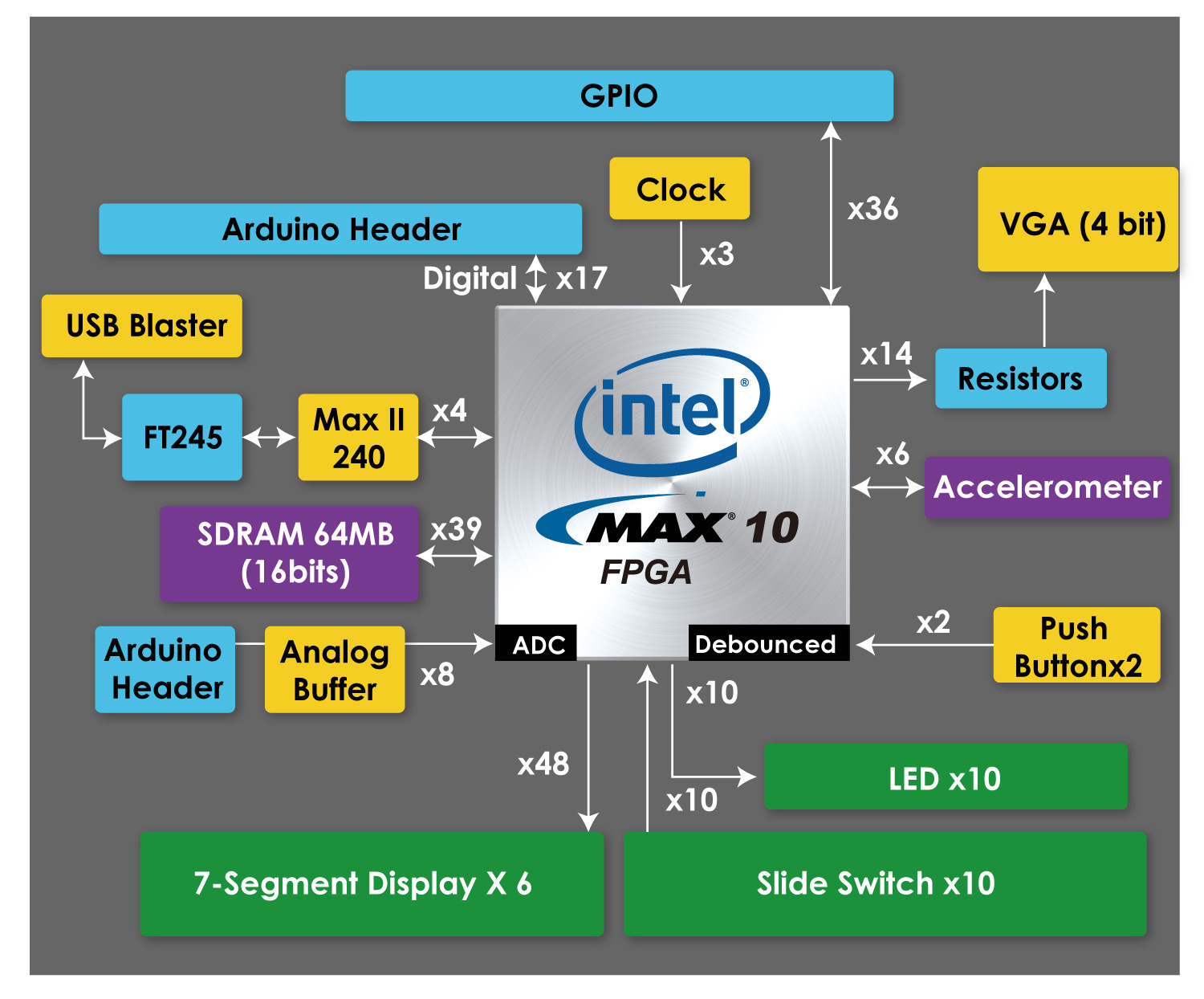
The project was implemented on a Terasic DE10-Lite FPGA board based on the Altera MAX 10 [1] that includes 50,000 Logic Elements, on-board ADC, USB Blaster, Accelerometer, GPIOs, and Arduino expanders. However, the scope of this project only required the usage of the GPIOs, the Logic Elements, and the onboard clocks. Additionally, the board also includes a 64MB SDRAM, x16 bits data bus.
The implementation of the project used the following peripherals available on board
- 10 LEDs
- 10 Slide Switches
- 2 Push buttons
- 7-Segment displays

Figure 1: Block Diagram of the DE10-Lite Board

Figure 2: The DE10-Lite board with values in the LEDs and the 7 segment display
The project was implemented using the principles of FPGA programming using the System Verilog Hardware Description Language and its paradigms. The Visual Studio Code IDE was primarily used in the development and writing of code for the project. Compilation of the design, including the Analysis and Synthesis, Fitting, Assembly, Timing Analysis, and Programming was done using the Quartus Prime - Lite IDE software.

Figure 3: Quartus Prime - Lite IDE specifications
The Five stages of the 5-stage RISC-V pipeline include:
- Instruction Fetch (IF): To fetch instruction from the memory and forward to the next stage
- Instruction Decode (ID): To decode the instruction and identify the operands
- Execution (EX): To perform the actual operation or computation of the instruction
- Memory Access (MEM): To access data from the memory, if required
- Write Back (WB): To write the result back to the register file system
In summary, the IF stage fetches the instruction, the ID stage decodes it, the EX stage executes it, the MEM stage accesses the memory (if needed), and the WB stage writes the result back to the register file. These stages are repeated for each instruction in the program. In addition to the five standard stages, each of which are programmed using a separate module, there are three additional modules in the project, they are
- DualPortRam module: The memory module
- IO: The module to handle the IO operations
- Register File System: The module to handle register file system
The pipeline stages work in parallel, allowing multiple instructions to be executed simultaneously. As one instruction is being executed in one stage, the next instruction can be fetched in the previous stage, resulting in a significant improvement in instruction throughput. However, the pipeline introduces the risk of hazards such as data hazards, control hazards, and structural hazards, which need to be addressed to ensure correct operation of the processor. The implementation can simply be summarized as in Figure 4.

Figure 4: Implementation block diagram
As seen in Figure 4, each interconnection between the blocks are representative of multiple data lines connected of widths ranging from 1 bit wide to 32 bit wide.
Following are the supported instructions by the current implementation
| Instruction | Type | Ex Operation |
|---|---|---|
| ADD | R | rs1 + rs2 |
| SUB | R | rs1 – rs2 |
| SLL | R | rs1 << rs2[4:0] |
| SLT | R | 1 if rs1 < rs2 (signed) 0 else |
| SLTU | R | 1 if rs1 < rs2 (unsigned) 0 else |
| XOR | R | rs1 XOR rs2 |
| SRL | R | rs1 >> rs2[4:0] (logical) |
| SRA | R | rs1 >> rs2[4:0] (arithmetic) |
| OR | R | rs1 v rs2 |
| AND | R | rs1 ^ rs2 |
| JALR | I | pc+4 |
| LB | I | rs1+signex(i[11:0]) |
| LH | I | rs1+signex(i[11:0]) |
| LW | I | rs1+signex(i[11:0]) |
| LBU | I | rs1+signex(i[11:0]) |
| LHU | I | rs1+signex(i[11:0]) |
| ADDI | I | rs1+signex(i[11:0]) |
| SLTI | I | 1 if rs1 < signex(i[11:0]) (signed) 0 else |
| SLTIU | I | 1 if rs1 < signex(i[11:0]) (unsigned) 0 else (2 disjoint ranges) |
| XORI | I | rs1 XOR signex(i[11:0]) |
| ORI | I | rs1 v signex(i[11:0]) |
| ANDI | I | rs1 ^ signex(i[11:0]) |
| SLLI | I | rs1 << shamt |
| SRLI | I | rs1 >> shamt (logical) |
| SRAI | I | rs1 >> shamt (arith) |
| FENCE | I | - |
| ECALL | I | - |
| EBREAK | I | - |
| SB | S | rs1+signex(i[11:0]) |
| SH | S | rs1+signex(i[11:0]) |
| SW | S | rs1+signex(i[11:0]) |
| BEQ | B | - |
| BNE | B | - |
| BLT | B | - |
| BGE | B | - |
| BLTU | B | - |
| BGEU | B | - |
| LUI | U | i[31:12]:12’b0 |
| AUIPC | U | i[31:12]:12’b0+pc |
| JAL | J | pc+4 |
Table 1: List of supported instructions
In this stage, the instruction is fetched from memory, the Dual Port RAM module and loaded into the iw_out instruction register. The program counter is incremented to point to the next instruction and is stored in the pc_out register and passed to the next stage. The signals originating from and arriving at the IF stage are summarised in Table 2.
| Signal | Type | Synchronicity Status | Width (bits) | Source/Destination (module) |
|---|---|---|---|---|
| clk | Input | - | - | Board |
| reset | Input | Synchronous | 1 | Board |
| memIfData | Input | Asynchronous | 32 | Dual Port RAM / Memory Interface |
| jump_en_in | Input | Synchronous | 1 | Instruction Decode |
| jump_addr | Input | Synchronous | 32 | Instruction Decode |
| memIfAddr | Output | Asynchronous | 32 | Dual Port RAM / Memory Interface |
| iw_out | Output | Synchronous | 32 | Instruction Decode |
| pc_out | Output | Synchronous | 32 | Instruction Decode |
| jump_en_out | Output | Synchronous | 1 | Instruction Decode |
Table 2: Signals in the Instruction Fetch Stage
In a synchronized manner, depending on the state of the reset signal, the PC is either incremented by 4 or reset to 0. Additionally, another check is performed to ensure if the instruction fetched in the previous cycle and decoded by the IF stage requires a jump. The signal indicating this is checked and the appropriate jump address is loaded into the iw_out register. Communication between the Dual Port RAM module is asynchronous so as to not delay the instruction fetch cycle and meet the timing constraints of the design.

Figure 5: Implementation of the IF stage
In this stage, the instruction word received from the Instruction Fetch stage is decoded to determine the operation to be performed and the operands to be used. Depending on the type of the instruction, the register file is read to fetch the values of the operands. Figure 6 summarizes the signals in the ID stage.

Figure 6: Signals in the ID stage
Additionally, the stage also implements Data Forwarding to handle Data Hazards by comparing the write-back register and the write-back signals forwarded from the EX, MEM and the WB stages of the previous three instructions with the rs1 and rs2 of the current instructions. If there is a match and if the write-back signal in the forwarded signals is high, then the rs1 or rs2 is updated to be the forwarded value instead of the one fetched from the Register File system. The control signals from each of the three subsequent stages are forwarded asynchronously and also checked asynchronously in the ID stage.
Instruction Decode stage also handles Branch Hazards by decoding the opcode first and determining if a jump is necessary. It must be noted that the rs1 and rs2 values used in determining the status of various jump instructions could possibly be the forwarded values from the three subsequent stages or from the ones fetched from the memory.
Upon detecting that a jump is required, a jump_enable flag is set and a jump address is calculated from the values in the opcode and both these signals are asynchronously passed back to the Instruction Fetch stage which takes appropriate action and performs the jump. The signals originating from and coming into the Instruction Decode stage are summarized in Table 3.
| Signal | Type | Synchronicity Status | Width (bits) | Source/Destination (module) |
|---|---|---|---|---|
| clk | Input | - | - | Board |
| reset | Input | Synchronous | 1 | Board |
| iw_in | Input | Synchronous | 32 | Instruction Fetch |
| rs1_data_in | Input | Synchronous | 32 | Register Interface |
| rs2_data_in | Input | Synchronous | 32 | Register Interface |
| jump_en_in | Input | Synchronous | 1 | Instruction Fetch |
| df_ex_enable | Input | Asynchronous | 1 | Execution |
| df_ex_reg | Input | Asynchronous | 5 | Execution |
| df_ex_data | Input | Asynchronous | 32 | Execution |
| df_mem_enable | Input | Asynchronous | 1 | Memory Access |
| df_mem_reg | Input | Asynchronous | 5 | Memory Access |
| df_mem_data | Input | Asynchronous | 32 | Memory Access |
| df_wb_enable | Input | Asynchronous | 1 | Write-back |
| df_wb_reg | Input | Asynchronous | 5 | Write-back |
| df_wb_data | Input | Asynchronous | 32 | Write-back |
| wb_en_out | Output | Synchronous | 1 | Execution |
| rs1_reg | Output | Synchronous | 5 | Execution |
| rs2_reg | Output | Synchronous | 5 | Execution |
| wb_reg | Output | Synchronous | 5 | Execution |
| pc_out | Output | Synchronous | 32 | Execution |
| iw_out | Output | Synchronous | 32 | Execution |
| rs1_data_out | Output | Synchronous | 32 | Execution |
| rs2_data_out | Output | Synchronous | 32 | Execution |
| w_en_out | Output | Synchronous | 1 | Execution |
| jump_en_out | Output | Asynchronous | 1 | Instruction Fetch |
| jump_addr | Output | Asynchronous | 32 | Instruction Fetch |
Table 3: Signals in the Instruction Decode Stage
In this stage, the actual operation is performed, using the operands obtained in the previous stage. The result of the operation is then stored in a temporary register, alu_temp. The value of the temporary register is latched on and passed to the next stage and forwarded back to the ID stage (data forwarding). The task of actually executing the received instruction is done asynchronously to ensure timing constraints are met and no delays are introduced.

Figure 7: Signals in the EX stage
An appropriate action is performed depending on the opcode, function-7 and the function-3 values received in the iw_in instruction word and the correct operands (rs1 and rs2) from the ID stage. Depending on the type of operation, the execution stage acts either on the operands rs1, rs2, manipulates the values of the Program Counter or calculates a register address as necessary.
If the reset button is pressed on the board, the reset signal will be synchronously passed through the stages and at the EX stage, all output signals will be cleared and set to default values (0 in most cases). If the reset signal is not active at the clock, the output signals will appropriately be updated with the values received from previous stages and the results of the EX stage. Three signals are asynchronously forwarded to the ID module for the purpose of Data Forwarding to handle Data Hazards. The signals originating from and coming into the Execution stage are summarized in Table 4.
| Signal | Type | Synchronicity Status | Width (bits) | Source/Destination (module) |
|---|---|---|---|---|
| clk | Input | - | - | Board |
| reset | Input | Synchronous | 1 | Board |
| wb_en_in | Input | Synchronous | 1 | Instruction Fetch |
| wb_reg_in | Input | Synchronous | 5 | Instruction Decode |
| pc_in | Input | Synchronous | 32 | Instruction Decode |
| iw_in | Input | Synchronous | 32 | Instruction Decode |
| rs1_data_in | Input | Synchronous | 32 | Instruction Decode |
| rs2_data_in | Input | Synchronous | 32 | Instruction Decode |
| w_en_in | Input | Synchronous | 1 | Instruction Decode |
| alu_out | Output | Synchronous | 32 | Memory Access |
| iw_out | Output | Synchronous | 32 | Memory Access |
| pc_out | Output | Synchronous | 32 | Memory Access |
| wb_reg_out | Output | Synchronous | 5 | Memory Access |
| wk_en_out | Output | Synchronous | 1 | Memory Access |
| w_en_out | Output | Synchronous | 1 | Memory Access |
| rs2_data_out | Output | Synchronous | 32 | Memory Access |
| df_ex_enable | Output | Asynchronous | 1 | Instruction Decode |
| df_ex_reg | Output | Asynchronous | 5 | Instruction Decode |
| df_ex_data | Output | Asynchronous | 32 | Instruction Decode |
Table 4: Signals in the Execution Stage
In this stage, the result obtained from the execution stage is written to memory or data cache if the instruction is a store instruction. If the instruction is a load instruction, the data is read from memory or data cache and written to a temporary register.
This is done asynchronously depending on the w_en_in signal and the 31st bit of the alu_output. alu_in[31] is set only if the instruction word was that of a Load instruction. This will cause the processor to read/write from/to the IO space, (the IO module in the design). If the two signal conditions are not met, the module will read/write from/to the memory space (the Dual Port RAM module).

Figure 8: Signals in the MEM stage
This module additionally generates another signal called the source_select. This signal will be synchronously passed on to the Write-back stage and will indicate the source of the data that must be written into the Register File System. The source can be one of the following three:
- IO space
- Memory
- ALU output Signals are passed onto the WB stage synchronously to ensure the timing constraints are accurately met. Three signals are asynchronously forwarded to the ID module for the purpose of Data Forwarding to handle Data Hazards.
| Signal | Type | Synchronicity Status | Width (bits) | Source/Destination (module) |
|---|---|---|---|---|
| clk | Input | - | - | Board |
| reset | Input | Synchronous | 1 | Board |
| wb_en_in | Input | Synchronous | 1 | Execution |
| pc_in | Input | Synchronous | 5 | Execution |
| iw_in | Input | Synchronous | 32 | Execution |
| alu_in | Input | Synchronous | 32 | Execution |
| wb_reg_in | Input | Synchronous | 5 | Execution |
| wb_en_out | Output | Synchronous | 1 | Write-back |
| pc_out | Output | Synchronous | 32 | Write-back |
| iw_out | Output | Synchronous | 32 | Write-back |
| alu_out | Output | Synchronous | 32 | Write-back |
| wb_reg_out | Output | Synchronous | 5 | Write-back |
| memif_rdata | Input | Asynchronous | 32 | Dual Port RAM |
| io_rdata | Input | Asynchronous | 32 | Dual Port RAM |
| rs2_data_in | Input | Synchronous | 32 | Execution |
| w_en_in | Input | Synchronous | 1 | Execution |
| memif_we | Output | Asynchronous | 1 | Dual Port RAM |
| memif_be | Output | Asynchronous | 4 | Dual Port RAM |
| memif_addr | Output | Asynchronous | 30 | Dual Port RAM |
| memif_wdata | Output | Asynchronous | 32 | Dual Port RAM |
| memif_rdata_out | Output | Asynchronous | 32 | Write-back |
| io_we | Output | Asynchronous | 1 | IO |
| io_addr | Output | Asynchronous | 30 | IO |
| io_wdata | Output | Asynchronous | 32 | IO |
| src_sel_out | Output | Synchronous | 2 | Write-back |
| df_mem_enable | Output | Asynchronous | 1 | Instruction Decode |
| df_mem_reg | Output | Asynchronous | 5 | Instruction Decode |
| df_mem_data | Output | Asynchronous | 32 | Instruction Decode |
Table 5: Signals in the Memory Access Stage
In this stage, the final result of the instruction is written back to the register file. This is the final stage of the pipeline before the next instruction is fetched. In the Write-back stage, the data to be written to the Register File System is determined by the src_sel_in signal received from the MEM stage. If a reset is received, the Write-back enable signal is cleared ensuring no data may be written to the Register File System. Table 6 summarizes the signals originating from the WB stage and coming into it.
| Signal | Type | Synchronicity Status | Width (bits) | Source/Destination (module) |
|---|---|---|---|---|
| clk | Input | - | - | Board |
| reset | Input | Synchronous | 1 | Board |
| wb_en_in | Input | Synchronous | 1 | Write-back |
| wb_reg_in | Input | Synchronous | 5 | Write-back |
| pc_in | Input | Synchronous | 32 | Write-back |
| iw_in | Input | Synchronous | 32 | Write-back |
| alu_in | Input | Synchronous | 32 | Write-back |
| memif_rdata | Input | Asynchronous | 32 | Dual Port RAM |
| io_rdata | Input | Asynchronous | 32 | IO |
| src_sel_in | Input | Synchronous | 2 | Write-back |
| wb_en_out | Output | Synchronous | 1 | Register File System |
| wb_data | Output | Synchronous | 32 | Register File System |
| wb_reg_out | Output | Synchronous | 5 | Register File System |
| df_wb_enable | Output | Asynchronous | 1 | Instruction Decode |
| df_wb_reg | Output | Asynchronous | 5 | Instruction Decode |
| df_wb_data | Output | Asynchronous | 32 | Instruction Decode |
Table 6: Signals in the Write-back Stage
In addition to the five modules for the five stages of the RISC-V pipelined architecture, there are three additional modules implemented to support their operations. These are:
- Register File System: Register storage system
- IO: Handle IO operations
- Dual Port RAM: Memory system
The design supports 32 general purpose registers including one always-zero register as outlined in the RISC-V architecture [4]. Values written may be written to a register only if the writeback_enable signal from the WB stage is a valid 1 and in synchronicity with the data and the register address. Additionally, the write-back register address points to the zero register, no data will be written to it. Writes to the register are synchronous while reads from it are asynchronous. Table 7 summarizes the register hierarchy.
| Register Name | Description |
|---|---|
| zero | Hardwired zero |
| ra | Return address |
| sp | Stack pointer |
| gp | Global pointer |
| tp | Thread pointer |
| t0 | Temporary/alternate link register |
| t1–t2 | Temporaries |
| s0 | Saved register/frame pointer |
| s1 | Saved register |
| a0–a1 | Function arguments/return values |
| a2–a7 | Function arguments |
| s2–s11 | Saved registers |
| t3–t6 | Temporaries |
Table 7: Register Hierarchy
The IO module maps addresses in the memory to physical IO ports that are present on the Board. The IO ports in particular that are available on the DE10-Lite MAX 10 FPGA board include 10 toggle switches, 10 monochrome LEDs and 2 push buttons. Of these, the operations and working of the LEDs and the push buttons have been extensively tested in this implementation.
In particular, the address 0x8000 0000h has been mapped to push button 1 (input) and address 0x8000 0004h has been mapped to the 10 LEDs as output. The implementation assumes that Inputs and Outputs are independent and unique and may not behave interchangeably, and therefore limits the operations at the addresses to only read or write respectively. Figure 9 shows the implementation block diagram of the IO module.

Figure 9: IO module implementation
This module is used to convert the endianness of data during reads and writes to a dual-port RAM in a RISC-V processor. It takes in a clock input and two address inputs, one for instruction port (RO) and the other for data port (RW). It also takes in a data input, which includes a write-enable signal (d_we), a byte-enable signal (d_be), and a 32-bit data input (d_wdata). The module outputs two 32-bit data values, one for instruction read data (i_rdata) and the other for data read data (d_rdata). The multi-dimensional packed array "ram" is initialized using a bitstream from the "ram.hex" file, which is used to initialize the M9K RAM modules. The always block with a posedge clock is used for instruction fetch, and the always block for data read/write is triggered by a posedge clock as well. The module uses bitwise operations to convert the endianness of data during writes to RAM and during reads from RAM.

Figure 10: Implementation block diagram of the Dual Port RAM module
- The implementation has certain difficulties in matching timing when using the 50MHz clock and specifically the IO module. If the requirement is to run the processor at 50MHz, the present implementation will need to be modified to not support IO operations. To overcome this, the 10MHz clock is used instead.
- The Dual Port RAM module requires two clock cycles at the start of a program execution before the right Program Counter (PC) and Instruction Word (IW) are fetched and passed to the Instruction Fetch (IF) stage. By observation, this is due to the time taken to sync the io_we signal between the Memory Access stage and the Dual Port RAM stage. As a work around, the first two instructions MUST be NOP (No-operation) stalls.
- Data hazards between Memory Read/Write operations are not handled in the implementation at present. To ensure this does not lead to any unexpected issues during execution two solutions may be proposed -
- Three NOPs must be inserted following each Store and Load instruction in the Assembly code itself (this will be implemented as a part of the architecture of the processor in the near term).
- Alternatively, care can be taken to ensure that a location manipulated by a Store or Load instruction is not accessed by other instructions for at least three clock cycles. This can be achieved by inserting instruction for other operations between two successive Memory/IO instructions.
[1] https://www.terasic.com.tw/cgi-bin/page/archive.pl?Language=English&CategoryNo=218&No=1021&PartNo=2#heading [2] https://www.terasic.com.tw/attachment/archive/1021/image/DE10-Lite_Blackdiagram.jpg [3] Figure 5, Figure 6, Figure 7, Figure 8, Figure 9, Figure 10 are generated images from the Quartus Prime - Lite NetList RTL Viewer tool [4] https://riscv.org/technical/specifications/