Repository navigation
DDR Memory Init
How DRAM is organised, why bringing it up needs a controller + PHY, what read / write / gate leveling actually does, and how retention skips all of it on a warm reset. Grounded in the Axxia (Lionfish / gen2) code under board/axxia/common.
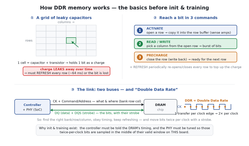
- A grid of leaky capacitors. Each cell is one capacitor + transistor holding a bit as a charge. Charge leaks, so every row must be refreshed (~every 64 ms) or the data is lost. Cells are organised into banks → rows → columns.
- Reach a bit in 3 commands: ACTIVATE opens a row into the row buffer (sense amps) → READ/WRITE picks a column (a burst of bits) → PRECHARGE closes the row. Plus REFRESH in the background.
- Two buses: CK + Command/Address says what & where (which bank·row·col, and ACTIVATE/READ/WRITE); DQ + DQS carries the actual bits with their own strobe. DDR = Double Data Rate: one transfer on each clock edge (↑ and ↓) → 2× per clock.
That last point is why init and training exist: at GHz the valid window for each bit is tiny, so the controller must be told the DRAM's timing and the PHY must be tuned to the board.
Two hardware blocks, two jobs:
| Controller (Denali) | PHY (Synopsys) | |
|---|---|---|
| Role | the protocol / brain | the electrical / muscles |
| Does | issues DDR commands, enforces JEDEC timing (CAS latency, tRCD, refresh), banks/ECC | drives the real pins: clock, strobe, data; impedance & delay-line calibration; tunes timing to the board |
| Domain | cycles & commands (digital) | picoseconds & volts (analog) |
The orchestrator is ncp_sysmem_init_synopphy() (board/axxia/common/ncp_sysmem_init_synopphy.c:3183), run per memory interface:
smId → smNode (0→0x22, 1→0x0f, 2→0x23, 3→0x24)
  ① ncp_sm_denali_2041_init_56xx()   init the CONTROLLER from the DRAM params
  ② ncp_sm_ddr4_phy_init()           PHY: PLL / ZCAL / DCAL, then DRAM reset + JEDEC init
  ③ ncp_sm_ddr4_phy_training()       the leveling pipeline (see §3)
  ④ ncp_sm_ddr4_post_phy_training_mc_setup()   hand the tuned link to the controller
The shared timing struct ctm is computed once (ncp_sm_common_setup_56xx) and passed to both the controller and the PHY, so their timing agrees.
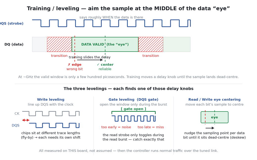
At ~GHz the valid window (the eye) is only a few hundred picoseconds, and the board routes CK / DQS / DQ at slightly different lengths (deliberately — "fly-by"). So the SoC can't assume when data lands; it must measure and set delays so every read/write is sampled dead-centre. Each step finds one delay knob:
- Write leveling — align DQS to CK at each DRAM chip (compensate the fly-by skew on writes).
- Gate leveling (DQS gate) — open the read "listen" window only while the read strobe is actually toggling (too early = noise, too late = miss).
- Read / Write eye centering (deskew) — nudge each data bit's sampling point to the centre of its eye.
- VREF — pick the voltage threshold that best separates 0 from 1.
Mechanically each step is the same: write the PIR (PHY Initialization Register) selecting one step, then poll PGSR0 for that step's done bit — in ncp_sm_ddr4_phy_training() (…ncp_sysmem_init_synopphy.c:1433). Order: WL → QSGATE → WLADJ → SRD → RDDSKW → WRDSKW → RDEYE → WREYE → VREF.
Training takes time and its result is board-specific, so on a warm / retention reset the DRAM is held in self-refresh (it keeps its own contents and calibration) and the destructive reset + full training is skipped. A persistent scratch bit flags it:
// board/axxia/common/axxia_initialize.c:86
ncr_read32(NCP_REGION_ID(0x156,0x00), 0x00dc, &value);
ddrRecovery = (value & 0x1);          // 1 = DDR retention recovery

// axxia_initialize.c:163
if (0 == ddrRecovery) {               // cold boot only:
        ... sysmem_init();            //   full DRAM reset + PHY training
}                                     // recovery: minimal re-init, RAM survives
Running the full sysmem_init() (with DRAMRST/DRAMINIT, …ncp_sysmem_init_synopphy.c:3000) on a recovery boot would wipe RAM — which is exactly what the ddrRecovery gate prevents.
| What | Where |
|---|---|
| orchestrator (per interface) | board/axxia/common/ncp_sysmem_init_synopphy.c:3183 |
| controller init (Denali 2041) | board/axxia/common/ncp_sm_denali_2041_init_56xx.c |
| PHY init (PLL/ZCAL/DCAL, DRAM reset+init) | …/ncp_sysmem_init_synopphy.c:2288 |
| training / leveling | …/ncp_sysmem_init_synopphy.c:1433 |
| retention gate | board/axxia/common/axxia_initialize.c:163 |
| entry from init path |
sysmem_init() → board/axxia/common/sysmem_asic.c:390
|
See also: SYSCACHE_ONLY_MODE — where, in SYSCACHE builds, this whole init moves from SPL into U-Boot (init_mem_axxia).