- DC operating point
- DC Sweep
- Transient analysis
- Frequency analysis
To simulate we need .cir files
- or asterisk is used for comments
.include 130nm_bulk.pm.txt
******Netlist part*********
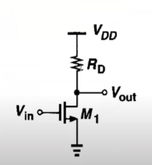
VDD net1 GND 1.5
RD net1 vout 10k
VG vin GND 0.6
** M1 Drain Gate Source Substrate
M1 vout vin GND GND NMOS W=1u L=130n
*****Analysis*******
.control
****DC Analysis*****
op
print @M1[id]
print @M1[gm]
print v(vout)
.endc
.end
.include 130nm_bulk.pm.txt

******Netlist part*********
VDD net1 GND 1.5
RD net1 vout 10k
VG vin GND 0.6
** M1 Drain Gate Source Substrate
M1 vout vin GND GND NMOS W=1u L=130n

*****Analysis*******

.control

***DC Sweep***
dc VG 0 1.5 0.1
plot v(vout)

.endc
.end
.include 130nm_bulk.pm.txt

******Netlist part*********
VDD net1 GND 1.5
RD net1 vout 10k
VG vin GND 0.6
** M1 Drain Gate Source Substrate
M1 vout vin GND GND NMOS W=1u L=130n

*****Analysis*******

.control

***DC Sweep***
save all @M1[id]
dc VG 0 1.5 0.1
plot @M1[id]

.endc
.end
.include 130nm_bulk.pm.txt

******Netlist part*********
VDD net1 GND 1.5
RD net1 vout 10k
VG vin GND 0.6
** M1 Drain Gate Source Substrate
M1 vout vin GND GND NMOS W=1u L=130n

*****Analysis*******

.control

***DC Sweep***
save all @M1[id]
save all @M1[gm]
dc VG 0 1.5 0.1
plot @M1[id]

.endc
.end
.include cmos_130nm.txt

******Netlist part*********
VDD net1 GND 1.5
RD net1 vout 10k
VG vin GND 0.6
** M1 Drain Gate Source Substrate
M1 vout vin GND GND NMOS W=1u L=130n

*****Analysis*******

.control

***DC Sweep***
save all @M1[id]
save all @M1[gm]
dc VG 0 1.5 0.1
plot @M1[id] vs v(vout)

.endc
.end
.include 130nm_bulk.pm.txt

******Netlist part*********
VDD net1 GND 1.5
RD net1 vout 10k
*VG vin GND 0.6
VG vin GND SIN(0.4 50m 10k)
** M1 Drain Gate Source Substrate
M1 vout vin GND GND NMOS W=1u L=130n

*****Analysis*******

.control

***small signal analysis***
tran 1u 0.5m
plot v(vout) v(vin)

.endc
.end
.include 130nm_bulk.pm.txt

******Netlist part*********
VDD net1 GND 1.5
RD net1 vout 10k
VG vin GND dc 0.3 ac 1
*VG vin GND SIN(0.4 50m 10k)
** M1 Drain Gate Source Substrate
M1 vout vin GND GND NMOS W=1u L=130n

*****Analysis*******

.control
*** AC/Frequency response
**Magnitude response
ac dec 100 1 100G
plot vdb(vout)
**phase response
plot ph(vout)
.endc
.end