Operations Physical Mods
What this page covers. Every documented hardware modification to the CMP 170HX: the PCIe AC-coupling capacitor mod that restores x16 link width, the soldering technique and tooling that make it succeed, how to verify the result, the teardown sequence, cooling and waterblock retrofits, the power connector situation, the strap resistors, and the things that a soldering iron categorically cannot fix on this card.
The headline result: the CMP 170HX trains at PCIe x4 because 12 of its 16 lanes ship with their AC-coupling capacitors depopulated from the factory. Hand-soldering 24 missing 0402 220 nF X7R capacitors restores a full x16 link, with no software patch of any kind. It is a beginner-to-hobbyist rework, reported at about 20 minutes per card by hand.
Warning
Width is not speed
The capacitor mod changes link width only. It never changes PCIe generation. A cap-modded card with no unlocker installed reports x16 at PCIe 1.0. Conversely, PCIe Gen2 (5 GT/s) has been reached purely in software on completely unmodified x4 cards. The two axes are independent and must never be conflated. For the speed half, see PCIe Gen2.
The CMP 170HX PCB is the NVIDIA A100 40 GB PCIe reference design with components deliberately
deleted. Every reference designator on the board matches the leaked NVIDIA Tesla A100 electrical
schematic NVIDIA-A100-GA100-883-P1001-B02-Rev-A.pdf (PG100/PG101 family). The board silkscreen
above the gold fingers reads 180-11001-DAAA-B15, 180-11001-DAAA-B35 and
180-11001-DAAA-045 across cards, the same family with a differing revision field. See
Board and variants.
The deletions are unpopulated VRM phases, missing NVLink interface ICs, a missing security-module region, and, critically, the missing PCIe AC-coupling capacitors on lanes 4 through 15. The traces are routed on the PCB. Only the parts are absent. NVIDIA populated exactly the 4 lanes the card was intended to use.
This is a board-level omission, not a fuse and not a firmware setting. The PCIe lane fuses are all clear on every 170HX probed:
| Fuse | Address | 170HX value | Meaning |
|---|---|---|---|
OPT_PCIE_LANE_DISABLE |
0x00820394 |
0x00000000 |
No lanes fused off |
CTRL_OPT_PCIE_LANE |
0x0082082c |
0x00000000 |
No lane override active |
STATUS_OPT_PCIE_LANE |
0x00820c2c |
0x00000000 |
Silicon reports full width available |
The link-status registers say the same thing. Stock lspci advertises x16 in capability and
negotiates down to x4 in status:
LnkCap:  Port #0, Speed 2.5GT/s, Width x16, ASPM not supported
LnkSta:  Speed 2.5GT/s, Width x4 (downgraded)
LnkCap2: Supported Link Speeds: 2.5GT/s
The (downgraded) marker on width is the tell: the endpoint is capability-x16 and trains x4,
which is exactly what a physical-layer discontinuity on 12 lanes produces. Independent
confirmation comes from a stock unmodified 8 GB card running the Gen2 branch, which reports
LnkCap: Speed 5GT/s, Width x16 while still showing LnkSta: Speed 5GT/s, Width x4 (downgraded):
software moved the speed and could not move the width. One host port that was itself x16-capable
still trained the card at x4.
| Attribute | Value | Notes |
|---|---|---|
| Quantity | 24 | 2 per differential pair × 12 depopulated lanes (lanes 4 to 15) |
| Package | 0402 | Metric 1005 |
| Capacitance | 220 nF (0.22 µF) | Design value from the A100 reference schematic |
| Dielectric | X7R | Frequently miswritten as "XR7"; the correct designation is X7R |
| Voltage rating | 6.3 V or higher | The x16 mod that is known to have worked used 6.3 V parts. These sit in series with a differential pair, and PCIe bounds transmitter DC common mode to 3.6 V, so 6.3 V carries ample margin |
| Confirmed part | Taiyo Yuden MAASJ105SB7224KFCA01 |
220 nF, 6.3 V, X7R, 0402, AEC-Q200. Twenty-four of these are what the first documented x16 mod used, and what a later four-card build used to reach Gen2 x16 on two board revisions (see Field report) |
| Confirmed substitute | Samsung Electro-Mechanics CL05B224KO5NNNC
|
220 nF, 16 V, X7R, 0402. Also reported working; its 16 V rating is incidental, not a requirement |
| Distributor number | DigiKey 1276-1176-1-ND; DigiKey 3886834 also cited |
Both plausibly map to the same manufacturer part in different packaging (cut-tape versus reel); neither is verified against the other |
| Reference designators | C1100 to C1350 range | Example grouping per differential pair: C1120, C1125, C1130, C1135 |
| Schematic source | NVIDIA A100 GA100-883 reference schematic P1001-B02, page 3, "IO: PCIe CONNECTOR" | The value is read off the A100 design, not measured on a 170HX |
Order spares. 0402 parts are trivially lost to tweezer flick and to solder-wick suction.
Note
Quote the manufacturer part, not the distributor number
Two different DigiKey numbers circulate for the Samsung substitute, and no source settles
which is correct; both may be valid for different packaging of the same part. Buy against a
manufacturer part, either MAASJ105SB7224KFCA01 (6.3 V) or CL05B224KO5NNNC (16 V), or
against the four-parameter specification (0402 / 220 nF / X7R / ≥6.3 V), and ignore the
distributor SKU.
The mod tolerates the general 100 nF to 220 nF decoupling class. One tester reported 100 nF 16 V X7R parts working. Another simply desoldered equivalent 0402 parts off a dead motherboard and
used those. Both are single first-hand reports. If you have the correct 220 nF part, use it: the
substitution evidence is thin, and a marginal AC-coupling network shows up as a training failure
that is indistinguishable from bad solder.
Adjudicated consensus from several people who solder professionally, including one explicit retraction of the opposite position.
| Parameter | Recommendation | Confidence |
|---|---|---|
| Solder alloy | 60/40 leaded | high |
| Flux | Gel flux | high |
| Prep | Wick away all factory lead-free solder first | high |
| Iron temperature | ~380 °C, fine point | high |
| Preheat | Not required | high |
| Hot air | Optional, faster for batches, correctly sized nozzle | high |
| Tweezers | Ceramic reverse tweezers, "tweezerable" but can flick 0.5 mm parts away | high |
| Masking | Kapton-tape the surrounding area | high |
| Low-melt alloy | Acceptable | medium |
| Practice | Do a scrap board first | high |
| Time per card | ~20 minutes by hand, experienced modder, imperfect result | medium |
The workflow that several people converged on: wick the pad pair clean of the factory lead-free solder, apply gel flux, tin one pad, place the part with tweezers and tack that side, then flow the other side. Solder paste applied with a needle plus a heat gun lets the parts self-align, which is the faster route for someone comfortable with hot air.
Caution
Do not preheat the whole board
Preheating the board in an oven was proposed in-channel and immediately rejected as a beginner trap. The documented real-world consequence of over-preheating (an IR stove plus hot air) is a bent PCB, broken internal traces and cooked ICs, producing subtle defects that are extremely hard to diagnose afterwards. This is the dominant beginner failure mode on this rework. A fine-point iron at 380 °C with no preheating is sufficient.
The 170HX x4 to x16 rework is beginner-to-hobbyist level. Experienced modders called it "probably the easiest card to do PCIE mod" and "way easier" than the CMP 100HX to V100 conversion, which needs full BGA equipment. The capacitor area is not cramped.
A separate caution recorded in-channel: the circulating a100-unlock.pdf /
cmp-170hx_a100_hardware-restore.pdf bill of materials includes a Winbond backup VBIOS chip
and other parts that have nothing to do with the lane mod. An experienced modder reading that
guide reasonably concluded it implied a full BGA job requiring a stencil. It does not. The PDF's
author stated that only the small components on the PCIe lanes are needed for x16; everything
else in that build was an attempt to replicate an A100 under the hood.
PCIe width negotiation falls back to the next legal width (16, then 8, then 4, then 1) rather than failing outright. That makes the reported lane count a direct diagnostic of solder quality.
| Capacitors correctly populated | Trained width |
|---|---|
| 0 of 24 (factory) | x4 |
| 12 of 24 | x8 |
| 12 to 23 of 24, or any bridged/cold joints | x8 |
| 24 of 24 | x16 |
An x8 result after a cap mod means incomplete or bridged solder work, not a distinct hardware limit. One modder's progression across three cards was x4, then x8, then x16 as technique improved. Another card came up x4, then x8, then x16 "after smaller readjustments". A third tester plateaued at x8 and speculated the link needed active load to widen; the better-supported explanation is cold or marginal joints.
The remedy is mechanical, not electrical: reflow and inspect all 24 joints under magnification, looking for tombstoned parts, solder bridges between the two pads of a pair, and joints that merely rest on the pad without wetting it.
Verify with LnkSta, never LnkCap. LnkCap is the advertised capability and can read
x16 (or Gen2) while the link is trained lower. That trap is the stated source of most "it works"
claims that do not hold up.
# 1. Find the card. Both SKUs enumerate as GA100 [CMP 170HX] (rev a1).
lspci -nn | grep -i nvidia
#   e.g. 0a:00.0 3D controller [0302]: NVIDIA Corporation GA100 [CMP 170HX] [10de:20c2] (rev a1)

# 2. The authoritative read: link status on the endpoint.
sudo lspci -s 0a:00.0 -vvv | grep -E 'LnkCap:|LnkSta:'

# 3. Kernel's own view, no root required.
cat /sys/bus/pci/devices/0000:0a:00.0/current_link_width   # want 16
cat /sys/bus/pci/devices/0000:0a:00.0/max_link_width       # 16
cat /sys/bus/pci/devices/0000:0a:00.0/current_link_speed   # 2.5 GT/s unless Gen2 is also applied

# 4. Driver's view.
nvidia-smi --query-gpu=pcie.link.gen.current,pcie.link.gen.max,pcie.link.width.current --format=csv
Expected transitions:
| State | LnkSta |
nvidia-smi gen.cur, gen.max, width |
|---|---|---|
| Stock, no mod, no unlocker | Speed 2.5GT/s, Width x4 (downgraded) |
1, 1, 4 |
| Capacitor mod only | Speed 2.5GT/s, Width x16 |
1, 1, 16 |
| Gen2 branch only, no mod | Speed 5GT/s, Width x4 (downgraded) |
2, 2, 4 |
| Capacitor mod + Gen2 branch | Speed 5GT/s, Width x16 |
2, 2, 16 |
Note that the (downgraded) suffix disappears from the width field once all 24 parts are in
place, which is the single clearest before/after signal.
Tip
(overdriven) on the speed field is normal
Depending on how Gen2 was applied, lspci may print
LnkSta: Speed 5GT/s (overdriven), Width x16. That suffix only means LnkSta reports a
higher speed than LnkCap advertises, which is exactly what happens when the link speed is
forced without rewriting the advertised capability. It is not an error and not instability.
See Verify for the full verification procedure and Troubleshooting for failure triage.
Tip
Test under load
Many platforms idle a link down when there is no traffic. If a width or speed reading looks wrong, re-read it during a bandwidth test rather than at idle.
| Configuration | Measured host bandwidth | Notes |
|---|---|---|
| Gen1 x4 (stock) | ~0.85 GB/s (send 0.80, receive 0.84) | OpenCL-Benchmark / clpeak |
| Gen1 x16 (cap mod only) | 2.88 GB/s flat, error-free | Nominal would be ~4 GB/s; the gap is attributed to PCIe 1.1 signalling overhead |
| Gen2 x4 (software only) | 1.68 GB/s send / 1.71 GB/s receive | OpenCL-Benchmark, one archived screenshot, unmodded card; the setup script independently predicts "~0.85 to ~1.7 GB/s, exactly 2x". Confidence medium |
| Gen1 → Gen2 on a cap-modded card that negotiated x8 | 1.67 → 3.24 GB/s | One A/B, single card, Asus Prime Z370 / i3-8100 / 8 GB RAM. Confidence medium. This is not a Gen2 x4 result: 3.24 GB/s exceeds the ~2.0 GB/s ceiling of Gen2 x4, because the card was running at x8 |
| Gen2 x16 (both) | 6.63 to 6.67 GB/s |
ocl_pcie_bw; nvtop showed TX 7.061 GiB/s at PCIe GEN 2@16x
|
| Gen2 x16 (both), second rig | 5.97 GB/s host-to-device, identical on all 4 cards | Four-card build on MAASJ105SB7224KFCA01, CUDA H2D, MaxPayload 256 bytes. Host-side difference from the 6.63 GB/s rig; both sit in the normal band for PCIe 2.0 x16 against an 8 GB/s ceiling. See Field report
|
Note
Gen2 x16: reproduced on a second rig
Gen2 x16 was first observed once, on 2026-07-26, on a single capacitor-modded card
running the unreleased Gen2 branch, at 6.63 to 6.67 GB/s, with no error telemetry and no
second rig. It has since been reproduced independently on four cards across two board
revisions, at 5.97 GB/s each, with lspci captures and zero AER errors after 90 minutes of
continuous four-card load. Confidence is now medium-high: two rigs, five cards total, and the
first actual stability evidence. Long-term burn-in beyond a few hours is still unmeasured.
See Field report.
A note on why lane count still matters even though speed is cheaper to obtain: platform lane budgets cap card count independently of bandwidth. A purely software Gen3 x4 unlock would need no soldering at all, which is why Gen3 x4 is the community's next target. It was described in-channel as speed-equivalent to Gen2 x16, but the arithmetic does not support that: Gen3 x4 is about 3.9 GB/s (8 GT/s, 128b/130b, four lanes) against Gen2 x16's 8 GB/s, so it lands nearer Gen1 x16. Either way, "lanes are lanes" for anyone packing many cards into one host. See PCIe Gen3 and Gen4.
For what link width does and does not do to inference throughput, see LLM inference and Performance. Pipeline-parallel inter-card traffic is negligible (a 5120-hidden-dimension model moves 10,240 bytes per token per hop, so roughly 25,000 tokens/s would be needed to saturate a single PCIe 1.0 lane), while tensor and expert parallelism were judged unworkable even at PCIe 2.0 x16.
The capacitor mod is invisible to the unlocker, and that is a verified negative rather than an
assumption. No file in shipping master or in any of the 12 unreleased branches contains the
strings "capacitor", "AC coupling" or "solder", nor any lane-width register. A grep over the full
git history returns nothing. The experimental Gen2 branch's 0007-pcie-gen2.patch manipulates
link speed registers only.
Note
Sourcing correction
A widely repeated claim states that the distributed unlock README documents the limitation as
"PCIe width is x4 (not x16): This is a hardware limitation of the CMP 170HX -- missing AC
coupling capacitors on lanes 4-15." The shipping README.md contains no such text, and
neither does any branch or any point in the git history. The technical claim is true and well
evidenced; only the attribution to the shipped README is wrong. It most likely originates in a
third-party guide.
A community member modified four CMP 170HX cards with twenty-four Taiyo Yuden
MAASJ105SB7224KFCA01 each (220 nF, 6.3 V, X7R, 0402) and supplied photographs and logs. All
four train PCIe 2.0 x16 and have run continuous four-card LLM inference with zero PCIe
errors. This is the second independent rig to reach Gen2 x16, after the single
2026-07-26 observation, and the first with more than one card, more than one board revision, or
any error telemetry at all.
Tip
Only the capacitors were fitted
No VBIOS was flashed: all four cards still report the stock 92.00.6D.00.0A. No VRM phases
were populated, no strap resistors were moved, no backup flash chip was added, and no other
footprint on the board was touched. The circulating a100-unlock.pdf bill of materials lists
a Winbond flash chip and a number of other parts; none of them were needed for x16. This
is direct confirmation of the PDF author's own later statement that only the components on
the PCIe lanes matter for lane width.
The populated AC-coupling rows on lanes 4 to 15, on board revision 180-11001-DAAA-B35. The
parts sit between the fan-out traces and the gold fingers, two per differential pair:
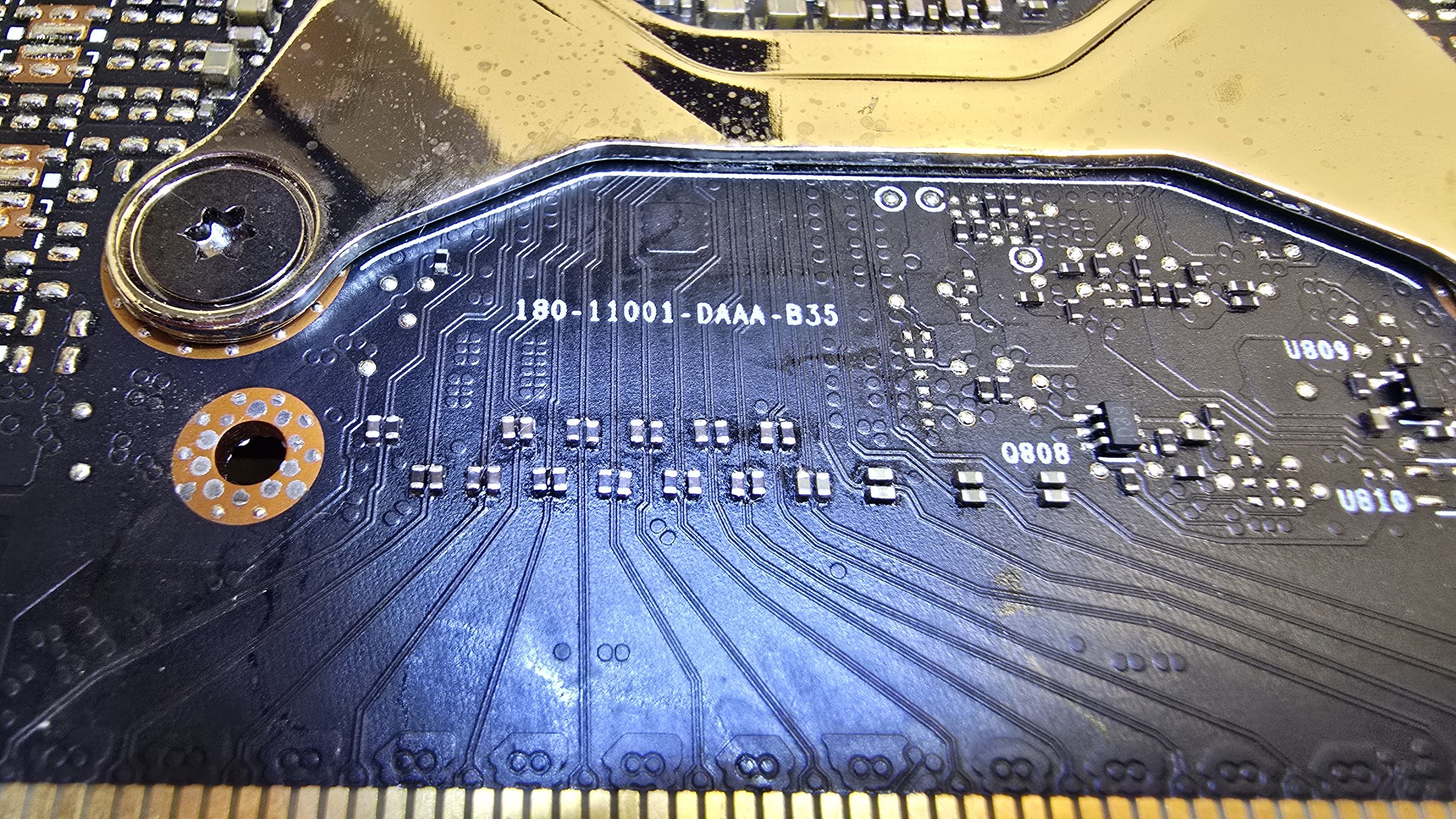
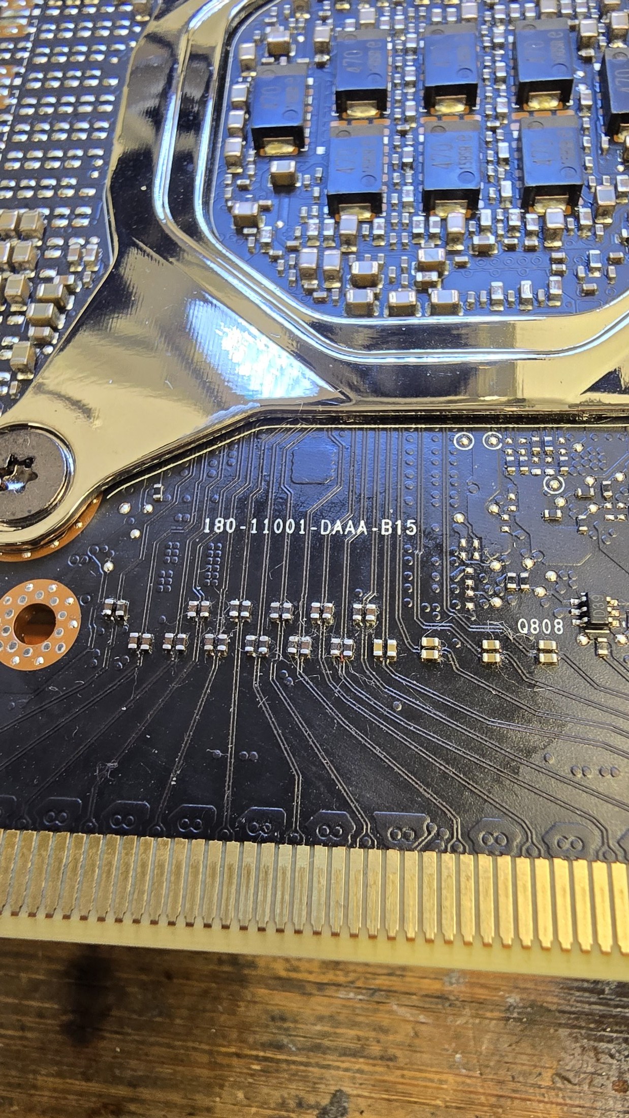
The same area on a 180-11001-DAAA-B15 board:
Wider views of both cards. The large arrays of unpopulated footprints across the middle of the board remain empty; only the capacitor rows beside the edge connector were populated.
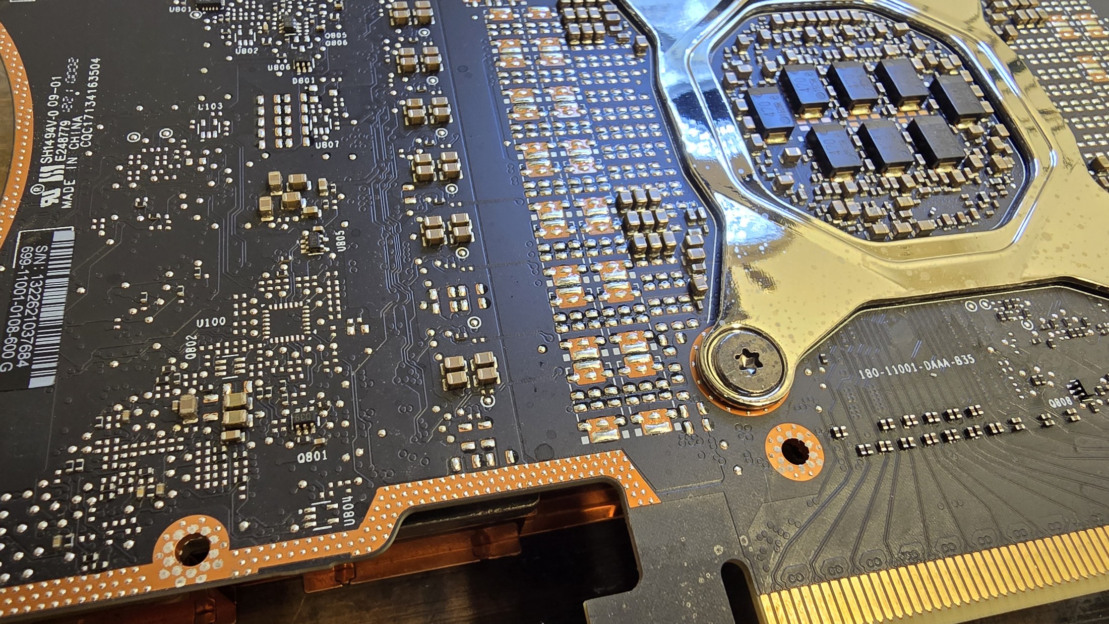
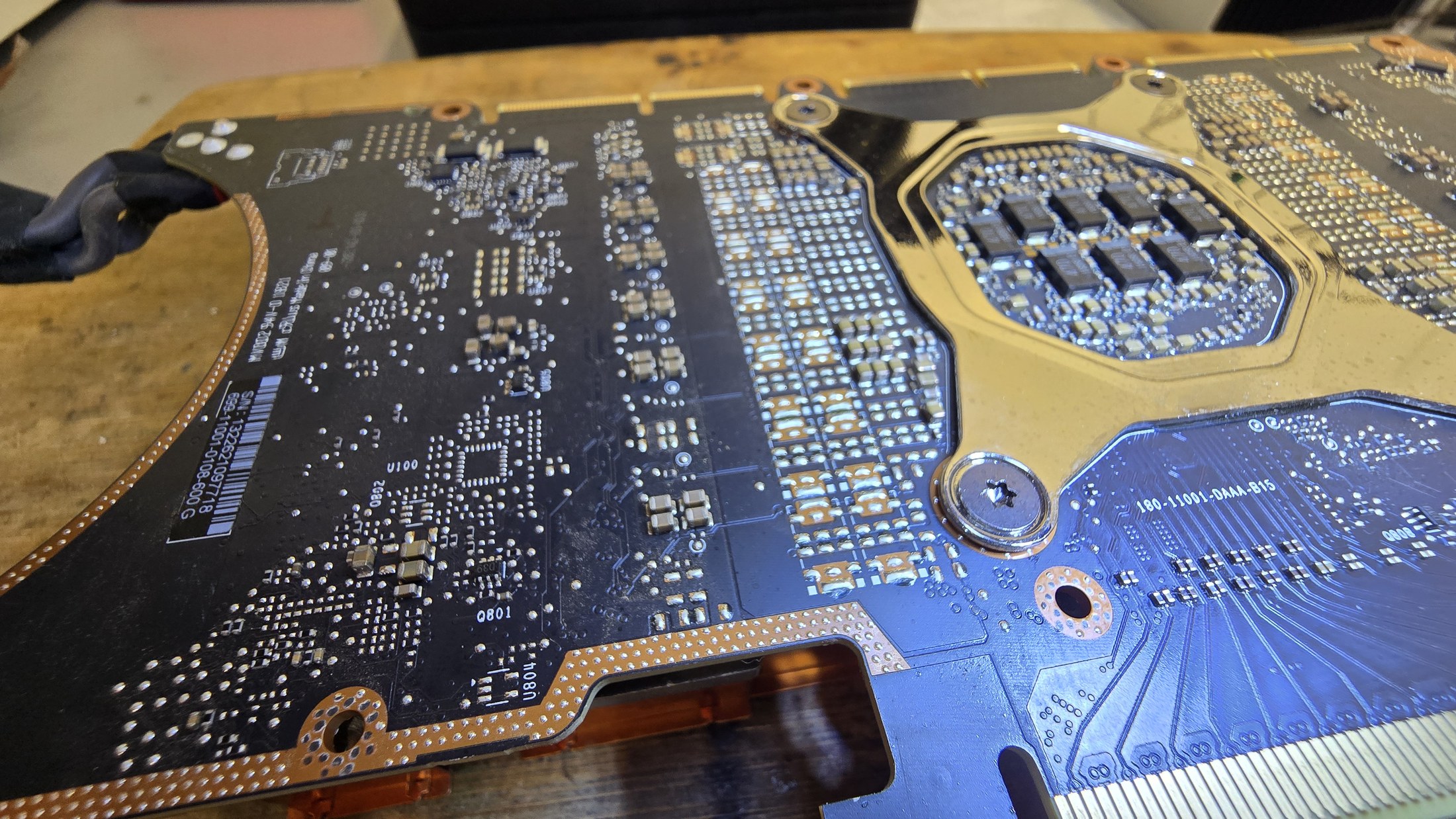
Two different silkscreen revisions were modified with identical results, 180-11001-DAAA-B15 and
180-11001-DAAA-B35, both carrying board part number 699-11001-0108-600 G. Revision B35 was
not previously recorded. All four cards are the 8 GB SKU running the 64 GB memory unlock, so
they report 65536 MiB.
All four cards, same host, capacitor mod plus the patched driver loaded with
NVreg_RegistryDwords="RmForceEnableGen2=1;RMPcieLinkSpeed=0x2":
LnkCap:  Port #0, Speed 2.5GT/s, Width x16, ASPM not supported
LnkSta:  Speed 5GT/s (overdriven), Width x16
LnkCap2: Supported Link Speeds: 2.5GT/s, Crosslink- Retimer- 2Retimers- DRS-
         MaxPayload 256 bytes, MaxReadReq 512 bytes
0000:03:00.0: width=16 speed=5.0 GT/s PCIe maxwidth=16
0000:04:00.0: width=16 speed=5.0 GT/s PCIe maxwidth=16
0000:88:00.0: width=16 speed=5.0 GT/s PCIe maxwidth=16
0000:89:00.0: width=16 speed=5.0 GT/s PCIe maxwidth=16
Note that on this rig the registry-dword route moves LnkSta only; LnkCap still advertises
2.5 GT/s, which is why lspci prints (overdriven) rather than a plain 5GT/s. An earlier
report of the Gen2 branch showed LnkCap: Speed 5GT/s instead. Either presentation is a
working Gen2 link. What matters is LnkSta, and specifically that Width x16 carries no
(downgraded) suffix.
Kernel AER counters after 90 minutes of continuous four-card inference:
0000:03:00.0: RxErr 0 BadTLP 0 BadDLLP 0 Rollover 0 Timeout 0 NonFatalErr 0 CorrIntErr 0 HeaderOF 0 TOTAL_ERR_COR 0
0000:04:00.0: RxErr 0 BadTLP 0 BadDLLP 0 Rollover 0 Timeout 0 NonFatalErr 0 CorrIntErr 0 HeaderOF 0 TOTAL_ERR_COR 0
0000:88:00.0: RxErr 0 BadTLP 0 BadDLLP 0 Rollover 0 Timeout 0 NonFatalErr 0 CorrIntErr 0 HeaderOF 0 TOTAL_ERR_COR 0
0000:89:00.0: RxErr 0 BadTLP 0 BadDLLP 0 Rollover 0 Timeout 0 NonFatalErr 0 CorrIntErr 0 HeaderOF 0 TOTAL_ERR_COR 0
Zero correctable errors and no fatal errors on any card. A marginal AC-coupling network or a cold
joint that still trains x16 would be expected to accumulate BadTLP or RxErr under sustained
traffic. Burn-in beyond 90 minutes has not been measured.
| Measurement | Result |
|---|---|
| Host-to-device, CUDA, per card | 5.97 GB/s, uniform across all four |
MaxPayload |
256 bytes (measured optimal on this host; 128 bytes cost throughput) |
MaxReadReq |
512 bytes |
Against a PCIe 2.0 x16 ceiling of 8 GB/s after 8b/10b encoding, 5.97 GB/s is about 75 percent, which is the normal range once TLP and DLLP overhead is accounted for. It is below the 6.63 to 6.67 GB/s recorded on the first Gen2 x16 rig; the difference is host-side (different root complex and chipset), not a property of the mod. The same 75 percent ratio appears in the Gen1 x16 figure of 2.88 GB/s against a 4 GB/s ceiling.
Required before waterblock installation, before reaching the SPI flash chip, and (on an assembled card) before any board-level rework. Fasteners are Torx T10 and T15.
- Remove the 4 PCIe mounting-bracket screws and save the bracket: it is reused as a spacer in the waterblock install. The bracket on the opposite side need not be removed.
- Flip the card and remove the 10 screws on the back.
- Flip again, open the front cover; the PCIe bracket comes off, revealing the heatsink.
- Unscrew the bracket holding the power cable and connector at the top right.
- Pry the stiff power cable free of the backplane with a plastic spudger. The board cannot move until the cable is freed.
- The hardest step. The PCB cannot be lifted vertically, because the PCIe connector slides into a slot in the backplane. Slide the board horizontally away from the connector until it clears by a few millimetres, then lift while continuing to move it horizontally. This step is documented as having defeated a well-known hardware channel on its first attempt.
- Remove the 4 spring-loaded screws on the back of the PCB and keep the 4 washers. They are not interchangeable with the plastic washers supplied with aftermarket waterblocks.
- Pry the heatsink off with a plastic spudger from a component-free edge, supporting it so it cannot fall onto the PCB.
Physical dimensions useful for planning: PCB 27 cm long, 29 cm all-in including the I/O shield and a plugged-in EPS connector; heatsink bolt pattern 57 × 68 mm centre to centre (68 mm vertical, 57 mm horizontal); die package about 55 × 55 mm.
Covered in operational depth on Cooling; this section covers the physical work only.
The Bykski N-TESLA-A100-X-V2 fits the A100 40 GB, CMP 170HX and A30 24 GB boards and uses
standard G1/4 fittings. It must be the V2 (all-metal) revision; the earlier non-V2 uses
transparent acrylic. Do not confuse it with the A100 80 GB block, which is incompatible.
Practical warnings from the one documented installation: the block ships with no user manual, only
a two-sentence online quick-start, and the included hex wrench is the wrong size, so bring a
metric hex set. A100-PCB waterblocks fit and expose the NVLink fingers.
Caution
Cover every unpopulated IC footprint before lowering the block
The single most damaging waterblock-installation mistake is leaving unpopulated IC footprints uncovered. The block's metal contact pillars can short across the exposed copper pads and permanently kill the card. Because the 170HX is a depopulated A100 board it has far more bare footprints than a real A100 and is correspondingly more dangerous to waterblock.
Pad every footprint within reach of a pillar: the DrMOS MOSFETs left and right of the ASIC; bottom-left and bottom-right of the ASIC; the PMIC to the right of the die between an inductor and a capacitor; and the two PMICs to the left of the die below the 3.3 µH inductor. Thermal paste (pea-sized) goes only on the GPU/HBM copper spreader.
Confidence note: the instruction is documented procedure and the mechanism is sound, but the causal attribution rests on one card that died about an hour after installation. The author's leading suspicion competes with a pre-existing mining-wear fault and with an omitted-bracket theory. It was never definitively isolated. Pad anyway.
Assembly specifics:
- Reuse the 4 original washers saved in teardown step 7, not the plastic washers supplied with the block, but use the waterblock's spring-loaded screws rather than the original screws.
- Install one spring screw first, then insert the power connector into the waterblock slot. The connector holder cover (item 4) must first be removed by unscrewing two hex nuts (item 5). Then fit the remaining 3 washers and screws.
- Reinstall the original PCIe slot bracket between the PCB and the backplane on the left as a spacer. Its additional height sets the spacing between backplane and board.
- The backplane is secured with four 9.5 mm M2 screws, two first, then two more.
- Finish with a 15-minute pressurised leak test before adding coolant.
Thermal interface on the stock cooler: 1.5 mm soft pads on the main areas and 3 mm soft on the inductors, plus a liquid thermal compound or liquid thermal pad on the die. A competing "2 mm" figure for the main pads was offered but prefaced with "I think" and is lower confidence; the T10/T15 bits are corroborated by both reports.
The 57 × 68 mm bolt pattern is close enough to an RTX 4080 heatsink or a socket-478/370 mount to allow retrofits; a 4080 heatsink was reported to fit "kinda". Two printed options circulate:
- The common 3D-printed shroud (
CMP_170HX_Fan_Shroud_Fixed.stl,CMP_170HX_Dual_Shroud_Fixed.stl) is friction-fit, falls off over time, and has walls thin enough to be weak even in PETG. Only STLs exist, so modifying it easily would need a STEP file. - The Level1Techs A-series blower adapter (
l1 a100 blower.stl, 52.3 KB, posted 2023-07-05) is a support-free print that bolts to the existing screw holes at the far end of the card, with an angled low section beside the power connector for finger access. Filament material, print settings, airflow direction and durability follow-up were asked in-thread and never answered.
Warning
Whatever cooler you fit must also cool the VRM
Die-only coolers leave the power stages unserved. One disputed field report describes cards that repeatedly blew a rear-board component after prolonged mining, with the suspicion that the operator was monitoring the core sensor (~56 °C) while overheating the VRM on a bandwidth-bound workload. An experienced long-time owner disputes that failure mode entirely. Unsettled, but the design rule stands regardless.
Note
Open problem
Do V100 vapour-chamber waterblocks fit the 170HX? Asked, never measured. Publish the 57 × 68 mm bolt pattern and 55 × 55 mm die dimensions against the block's spec sheet before buying. Related known-good data: SXM3 radiators are interchangeable with SXM2 with minor modifications. Caution: the 170HX card body is thick, so generic NVIDIA blower ducts may not fit.
The card takes a single EPS 8-pin, not a PCIe 8-pin. Most PSU-integrated EPS cables have
oversized retention clips that physically will not fit, so a 2× PCIe-8-pin-to-EPS adapter is
the usual solution. A modular EPS12V cable must carry 4× 12 V and 4× GND on both ends, and one
good-quality pin carries only about 70 to 80 W. Slot power limit from DevCap is 75 W; TDP is
250 W, and 300 W is not a software ceiling: on stock firmware the maximum equals the default, so
nvidia-smi -pl can only lower the card between 100 W and 250 W. Only the NVIDIA-issued 300 W
"OC mining" VBIOS raises the ceiling, and only on cards that carry it. See
Power and PSU.
Caution
Never performed, never measured
Restoring full A100 TDP is expected to be a simple shunt mod rather than a firmware change. Nobody in the corpus performed or measured one. The assessment is expert judgement from an experienced hardware modder and is plausible for this class of card, but the shunt locations, the resistor values, the resulting power figure and the thermal consequences are all unknown. A software or VBIOS route to a 400 to 500 W limit was proposed as the alternative for people uncomfortable with shunt modding, and was also never achieved. Attempting a shunt mod on this card is unmapped territory with an obvious path to destroying it.
An unpopulated 4-pin pad on the PCB was measured carrying 12 V and is suspected to be a fan header.
Note
Open problem
Nobody established the mating receptacle part, whether a tachometer line is present, or whether it is PWM-controllable. Wanted because it would enable standalone per-card fan control with no external controller. Next step: scope the remaining two pins at idle and under load, and trace them on the leaked schematic.
The board carries five strap resistor pairs in the top-left area near the decoupling capacitors: ten pads for five straps, unmarked parts, typically 100 kΩ 0402, pulled to 0 V or 1.8 V. Each strap is one resistor plus one empty pad, so moving the part between positions flips that strap bit. Reading left to right on the PCB:
| Strap | Designators | Function |
|---|---|---|
| Strap1 | R986, R987 | RAMCFG[1] |
| Strap0 | R989, R990 | RAMCFG[0] |
| Strap3 | R993, R994 | VGA_DEVICE |
| Strap4 | R999, R1000 | PCIE_CFG |
| Strap2 | R1004, R1005 | RAMCFG[2] |
R1004 and R1005 are the two alternative footprints of the same strap position, not two separate resistors. A sixth strap, DEVID_SEL at R240/R241, is named in the same source but has never been physically located.
Stock patterns: the A100 40 GB and the 170HX 10 GB share LLLLH; the 170HX 8 GB is HHLLH.
Caution
One strap pattern bricks the host
LLHHH on a 10 GB card produced no POST at all. Copying the A100's full strap
configuration onto a 170HX resulted in card not detected at boot. Strap experiments are
reversible in principle, but you can lose a working system to one until you move the part
back.
Note
Open problem
What do Strap3 (VGA_DEVICE, R993/R994) and Strap4 (PCIE_CFG, R999/R1000) actually do? Asked
2026-07-26, never answered. One accidental data point exists: a tester who intended to move
R1004 in fact moved Strap4, taking LLLLH to LLLHH, and reported no memory effect. Whether
PCIe capability negotiation changed was never measured. Next step: repeat that experiment
deliberately and capture lspci -vv LnkCap/LnkSta before and after.
Note
Open problem
Locate R240/R241 (DEVID_SEL) on the physical board. The device ID is what the shipping driver
keys geometry off, and OPT_DEVID_SW_OVERRIDE_DIS @ 0x00820584 = 0x00000001 closes every
software route to changing it. Search heuristic, sound and untried at scale: find a resistor
with an empty pad directly next to it, in the 200-series designator region, on the PCB side
that carries sub-500 designators. Asking a commercial AI assistant produced a confident,
entirely fabricated board topology and is recorded as a cautionary data point.
There is no OS-level flash path for this board. Writing the VBIOS means putting a chip clip on the SOIC part directly, which requires removing the heatsink, but no board passives need modifying to write with a clip.
Caution
Write-protect before power-on
Flashing failure 0xBADF3000, with the board unable to read flash, is caused by not
write-protecting the SPI chip before powering back on. Recovery is to reflash the SOIC
directly with a chip clip and then set write protection. The related symptom is an RM init
adapter failure. Confidence: medium (advice from someone who had done SOIC and VRM work on
these boards; the reporting user recovered the card shortly afterwards). See
Recovery and VBIOS.
The Winbond BIOS chip in the circulating hardware-restore bill of materials is a backup VBIOS chip for recovering from a bad flash. It is not part of the PCIe or memory unlock.
These boundaries are burned into fuses or into the package, and they bound every hardware idea on this page. Details in Fuses and OTP.
| Limit | Mechanism | Why solder does not help |
|---|---|---|
| SM count 70 (5 GPCs, 35 TPCs, CC 8.0) |
OPT_GPC_DISABLE 0x00820350 OTP |
Every per-GPC CTRL_OPT (0x00820838 + i*4) and RECONF_OVR (0x00820a40 + i*4) already reads 0x00000000; the enumerated count equals the fuse floor exactly. Nothing is being held back |
| Memory capacity ceiling |
FUSE_FBP_DISABLE 0x00820364, FUSE_FBPA_DISABLE 0x00820368, FUSE_FBIO_DISABLE 0x0082036c, ROP_L2_DISABLE 0x008202c4
|
The corresponding DEFECTIVE registers all read 0x0, so there are no real silicon defects, only an active disable mask; writing 0 to the DISABLE registers does not move them |
| Dead HBM stacks | Bonded to the silicon interposer, not the PCB | Reflow cannot work. One member spent several hours at a range of temperatures with a heat gun on several HBM2 GPUs, with no success. HBM stacks also contain internal fuses, so faulty dies can be permanently fused out inside the stack |
| NVLink |
FUSE_NVLINK_DIS plus unpopulated interface ICs |
The edge fingers are physically present and A100 waterblocks expose them, but bringing NVLink up would need the missing ICs and a fuse that is set. Plausibly the interposer itself carries eFuses. See NVLink |
| ECC | Fused off, no lever, no telemetry | See ECC |
| Display output | No display hardware on the board | Display pads exist on some CMP boards but would need "a ton of missing SMD components"; on the 170HX it is recorded as permanently absent |
| Device ID |
OPT_DEVID_SW_OVERRIDE_DIS 0x00820584 = 0x00000001; DEVIDA/DEVIDB fused on-die, selection strap-latched |
Software cannot override it and the selecting strap has never been located |
The accurate general statement, correcting an early flat "hardware unlock is impossible" verdict: hardware modification cannot move fused boundaries, but it can restore depopulated PCB features. The capacitor mod is the one place where that distinction pays.
The CMP 100-210 (a V100-class part) conversion to V100 or Titan V requires both a
strap-resistor move and a force-flash, in that order: on the strap array, move the existing
resistors from the bottom pads to the top pads to obtain HHLLHH (stock reported as HLLLHH or
HLLHHH), then force-flash the official Tesla V100 16 GB VBIOS with omgvflash. No different
resistor values are needed, only relocation. Flashing alone was tested and fails: the card
enumerates but the device ID is unchanged, so the Linux driver binds it as a CMP 100 and loads
incorrect binary blobs. Confidence: medium for the full procedure (one person with photos and
multiple successful units, no second party completed it in-log); high for the
"flashing alone is insufficient" half, which was directly tested.
Warning
The capacitor result does not transfer to the CMP 100-210
Lane count on the 170HX is purely a capacitor question (soldering alone gives x16 with no software at all, confirmed by several parties). A competing report on the CMP 100-210 says adding capacitors near the PCIe slot did not unlock x16 there, and that lane count is also software-gated on that card. Different silicon; there is no reason the answers must match, but the 170HX claim circulates without that qualifier.
By late July 2026 a large Shenzhen supplier offered the capacitor mod as a service for 1000 RMB (about $140) on Xianyu. Cap-modded cards listed at 8800-9800 RMB against 7000-7500 RMB unmodded; on Alibaba, about $1500 against roughly $1150-1300, so about a $300 premium, and one seller confirmed x16 as the reason.
Warning
Buyer warning: two different things cost about $1500
A separate ~$1500 tier from a different supplier is refurbishment, not the cap mod. Ask which tier you are being sold. Some Xianyu listings also charge extra for a bundled "cracked system disk", which is a pre-built unlock boot image. In-channel reports warn that inexperienced buyers attempting the mod themselves are likely to brick cards by improperly soldering the decoupling capacitors.
The Shenzhen service price is not the floor. One builder had their cards done at a local electronics repair shop for about $50 per card, roughly a third of the 1000 RMB service charge, with no shipping and no card leaving the country.
The hard part is not the soldering, it is finding someone willing to do it. That builder was turned away by more than ten shops before one agreed to simply fit the parts without arguing about it. Expect refusals: shops commonly want to diagnose the card first, dispute that missing capacitors are the real fault, or decline to work on hardware they did not sell. The job itself is unremarkable by board-repair standards, which is what makes the refusal rate surprising.
Guidance that follows from that, rather than from any measurement:
- Ask for the work by description, not by explanation. "Populate 24 0402 capacitors on these marked pads, parts supplied" is a quotable job. Explaining that it unlocks PCIe lanes on a mining card invites a debate about whether it will work, which is how the refusals start.
- Supply the capacitors yourself. The full set costs a few dollars and it removes any sourcing objection. See the bill of materials.
- Board-level micro-soldering and phone-repair shops are a better target than general PC repair. They already own the hot air, the microscope and the flux, and 0402 work is routine for them.
- Accept that the shop will not warranty the outcome. It cannot: whether the link trains x16 depends on the card, not on the solder joints alone.
At $50 per card this undercuts both the 1000 RMB service and the roughly $300 premium charged for a pre-modded card.
- PCIe subsystem: the link, its registers, and the fuse evidence
-
PCIe Gen2: the software half, patches
0007and0008 - PCIe Gen3 and Gen4: why the next step up is categorically harder
- Board and variants: silkscreen, SKU identification, depopulation inventory
- Cooling and Power and PSU: operating the modified card
- Fuses and OTP: the hard physical boundary
- Dead ends: every hardware idea that was tried and failed
- Risks: read before touching the board