Hardware Guide
[caption id="attachment_2298" align="alignnone" width="800"]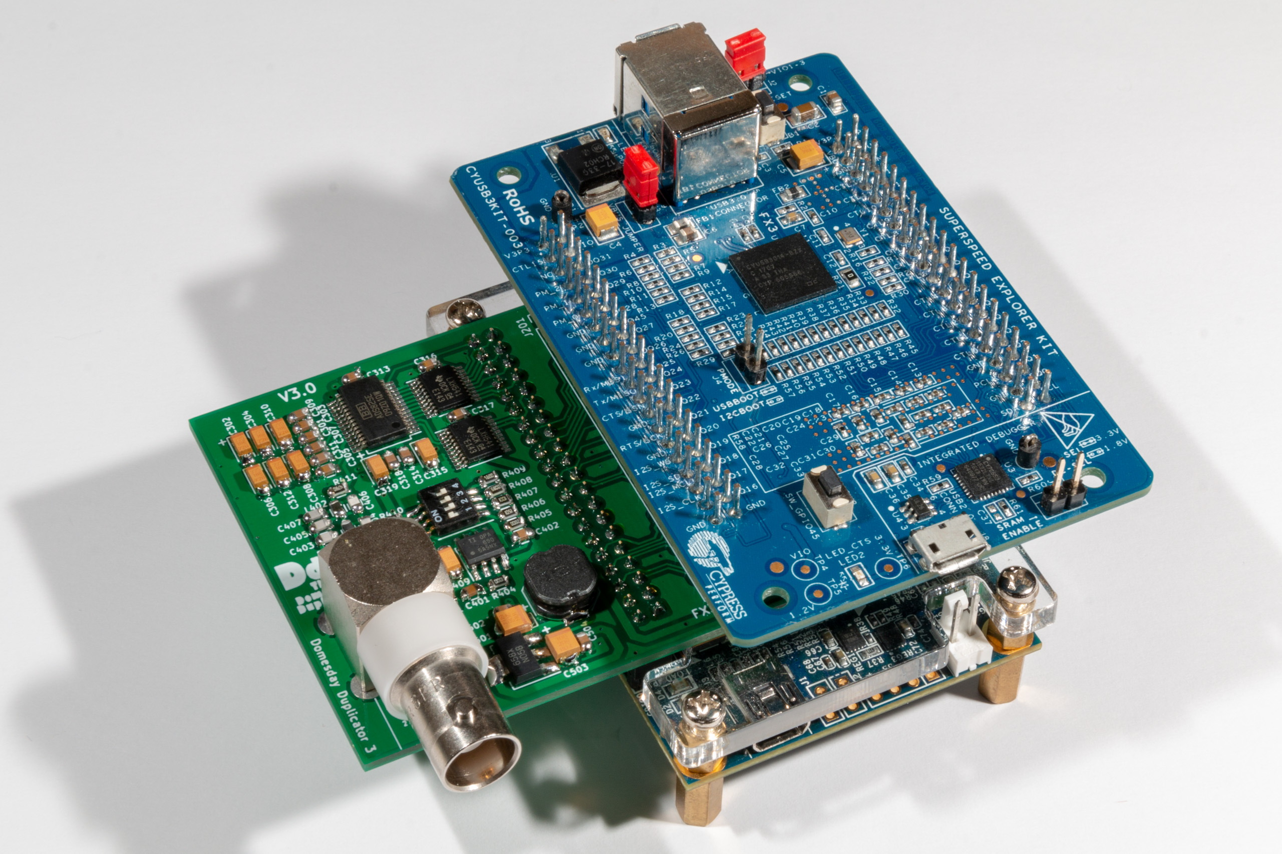
The Domesday Duplicator 3.0 design is split logically over 5 schematic pages. The following sections describe each schematic along with details of the design and how it functions. The Domesday Duplicator is designed specifically for the digitization (sampling) of RF spectra generated by a LaserDisc player when reading both NTSC and PAL LaserDiscs. For a non-technical overview please see the project overview page.
The expected signal for NTSC LaserDiscs is shown in the following diagram: [caption id="attachment_1388" align="alignnone" width="800"]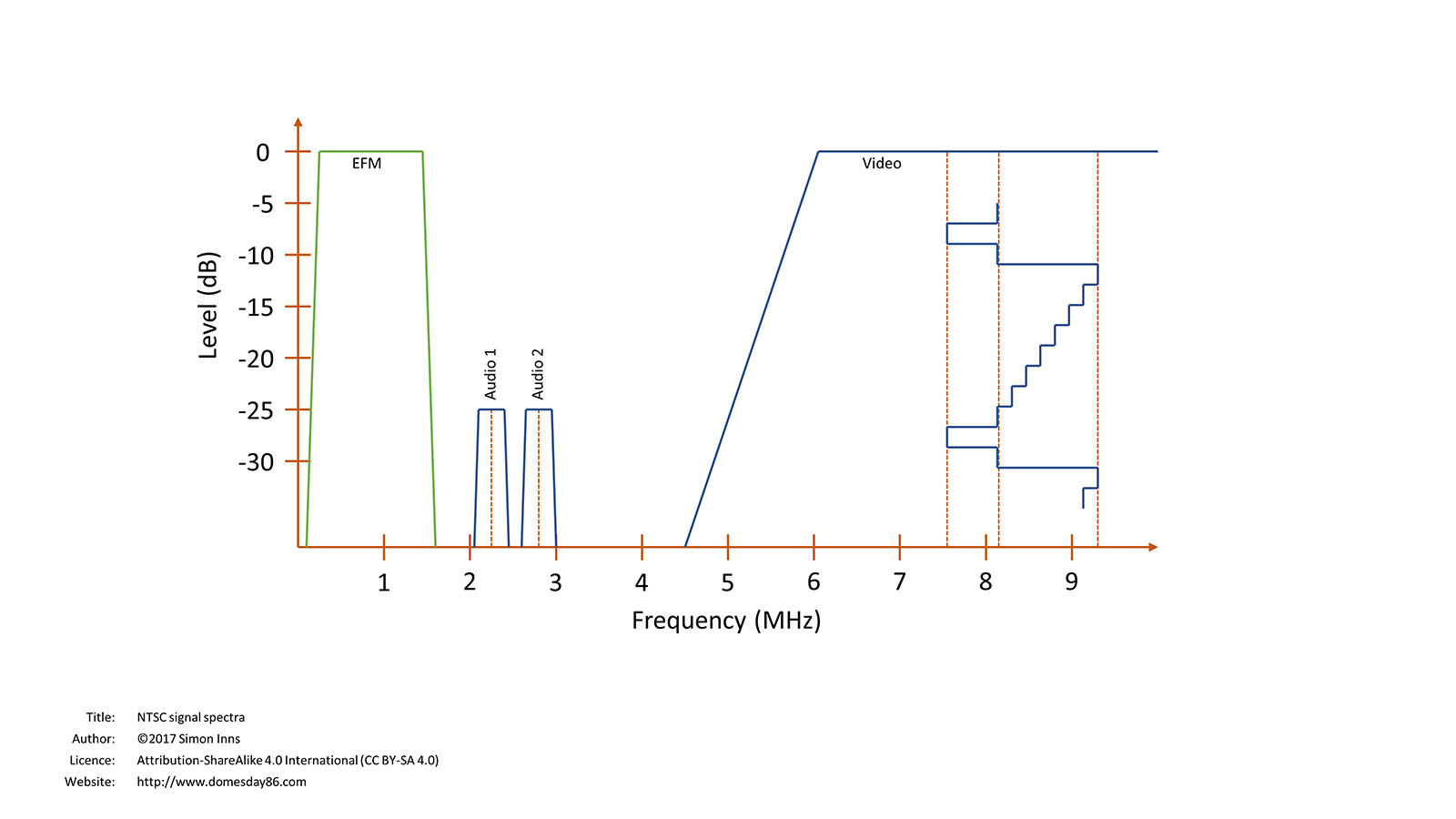
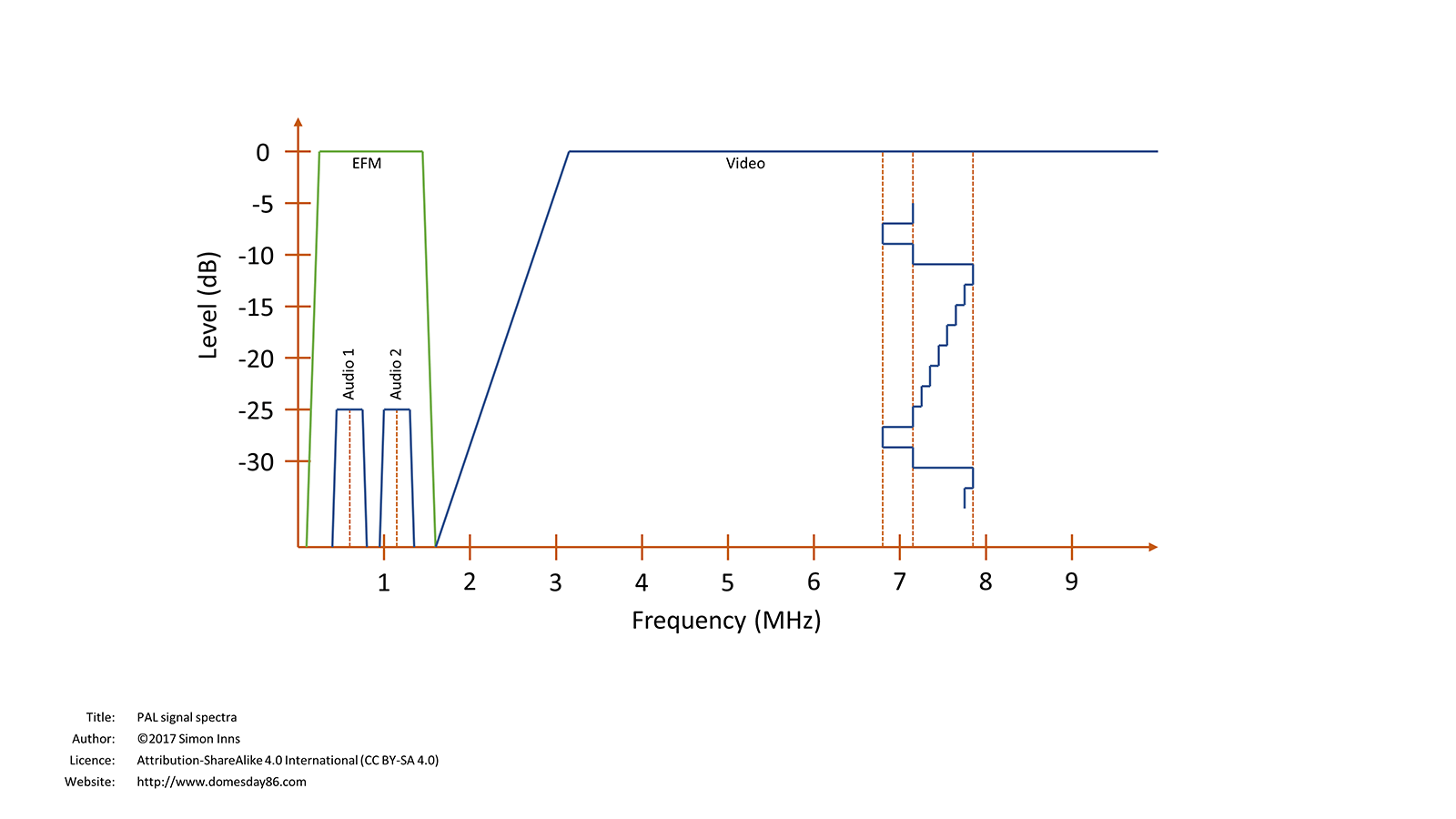
The expected input signal to the Domesday Duplicator is a 50 Ohm impedance source. The Domesday Duplicator gain and other amplitude measurements are based on this impedance. When measuring the amplitude of signals care should be taken to match the impedance of the test equipment to the signal impedance under test (this includes measuring the RF amplitude from LaserDisc players to select the correct gain on the Domesday Duplicator). To measure the peak-to-peak output from a LaserDisc player connect the RF output from the player to the Domesday Duplicator using a BNC T-adaptor, then connect the oscilloscope probe to the T-adaptor using a BNC probe adaptor. This will ensure that the RF signal is correctly terminated and the oscilloscope will show the correct peak-to-peak amplitude (as seen by the Duplicator itself).
The overview schematic shows the high-level interconnection of the 4 child-schematics consisting of:
- RF Amplifier
- ADC (Analogue to Digital Converter)
- Cypress Superspeed Interface (USB 3.0)
- Power supply
The schematic is shown in the following diagram: [caption id="attachment_2237" align="alignnone" width="800"]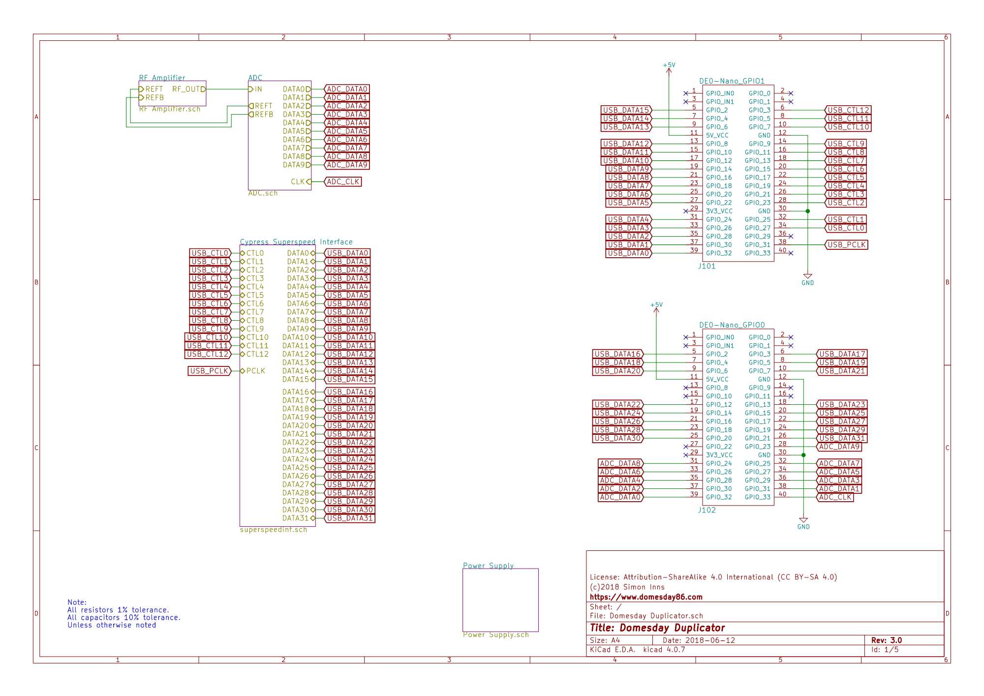
The RF Amplifier provides two basic functions. Firstly it amplifies the LaserDisc RF signal to the appropriate levels for the ADC (including setting the DC offset of the signal correctly for the ADC). Secondly it filters the RF signal using a low-pass filter to remove signal frequencies above the supported Nyquist limit of the ADC. The RF Amplifier schematic is shown in the following diagram: [caption id="attachment_2239" align="alignnone" width="800"]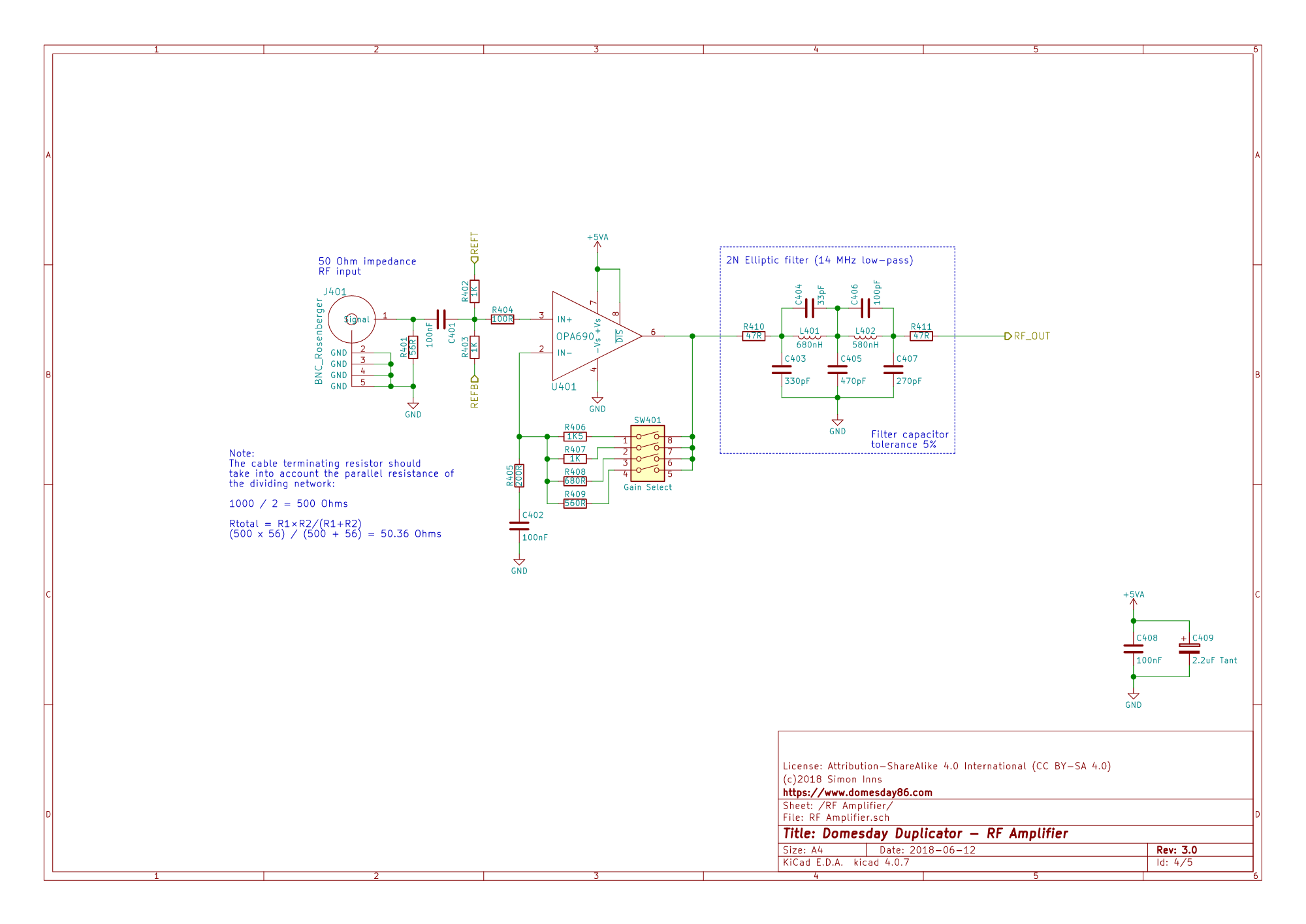
The input stage of the RF Amplifier is responsible for setting the impedance of the input from the RF source as well as removing any DC offset from the source signal and applying the required DC offset for the amplification stage.
The initial resistor R401 sets the overall impedance of the input however, the resistance of R401 is changed due to the presence of R402 and R403. The actual input impedance is the parallel resistance caused by the three resistors. This means that, in order to provide a 50 Ohm impedance, R401's value must be modified to account for the overall impedance. As R402 and R403 form a voltage divider the resistance at the centre-point of the divider is half the overall resistance of the resistor (i.e. 1000 Ohms / 2 = 500 Ohms). Ohm's law can be used to specify the overall impedance by calculating the parallel resistance between R401 and the 500 Ohm voltage divider: (500 x 56) / (500 + 56) = 50.36 Ohms. As the impedance of a LaserDisc player's RF test-point is typically 47 to 50 Ohms, this provides a close match across the expected range. For the purposes of calculation a 50 Ohm impedance is assumed by the rest of this description.
The DC offset of the incoming RF signal is removed by C401. Resistors R402 and R403 form a voltage divider between the reference top and reference bottom voltages (provided by the internal reference of the ADC). This places the DC offset at 2.5V which is the centre-point of the amplification stage. This same DC offset is used by the ADC removing the need to further correct the DC offset after amplification (therefore simplifying the circuit).
The amplification stage is fed the DC corrected RF signal via R404 (which provides some resistance to the input of the operational amplifier IC as recommended by the data-sheet). The operational amplifier is configured as a non-inverting amplifier with the linear gain set by the resistance between the op-amp output and the inverted input. The operational amplifier is a Texas Instruments OPA690 selected due to its high bandwidth (over 100 MHz) and rail-to-rail operation from a single supply (i.e. using ground and 5Vs only). The gain of the amplification stage is set by the combination of R405 to R409. The exact combination of resistors is user-selectable using a 4 way DIP switch that acts to make and break connection physically to the 4 resistors R406 to R409 (note: R405 is always included in the circuit).
Within the circuit R406 to R409 act as a single resistor providing one side of the gain calculation (identified as 'A' in this text). The other resistor R405 provides the second gain setting resistance (identified as 'B' in this text). The OPA690 data-sheet provides a set of rules for setting the linear gain of the operational amplifier: The individual resistance of both A and B should be greater than 200 Ohms and less than 1500 Ohms. The parallel combination of A and B should be less than 300 Ohms ( (A * B) / (A + B) = parallel combination resistance). So, (220 * 1200) / (220 + 1200) = 185.92 Ohms for example. The overall gain is given by 1+(A / B), so and example calculation would be 1+(1500 / 200) = 8.5. Note that the gain calculation is linear.
Gain configuration is provided using a 4-way DIP switch which allows the user to connect from one to four resistors in parallel. This configuration is used as a low-cost form of Variable Gain Amplifier (VGA). As the Domesday Duplicator uses a relatively high RF frequencies, solutions such as digital potentiometers do not provide the required bandwidth. Specialised ICs for variable and programmable gain do exist, however are cost prohibitive and generally require a fully differential ADC configuration. By using a carefully chosen set of resistor values along with a small footprint switch the amplification stage can provide 15 configurable gain settings that require only a few passive components to implement (keeping both the cost and signal noise to a minimum). The resistor values for R406 to R409 are selected due to the gain setting rule that the resistors A and B must both be between 200 Ohms and 1500 Ohms. The values 1500, 1000, 680 and 560 Ohms allow the maximum value for A (by selecting only the 1500 Ohm resistor) and the minimum value for A due to the parallel resistance combination of all four values: 1/R = (1/1500 + 1/1000 + 1/680 + 1/560) = 203.13 Ohms Once the maximum and minimum allowed values are established (by one resistor and all four resistors together), the other 13 configurations are formed by the other possible switch settings. To represent the various configurations it is useful to consider the 4 available switches as binary forming the numbers 0 to 15 (note: 0 is not a valid configuration as all resistors are disconnected, leaving 1-15 for use). The following table shows the configuration number, the switch position and the linear gain for each possible configuration (in order of increasing gain):
Configuration
Switches
Gain
15
1111
2.02
7
0111
2.17
11
1011
2.27
13
1101
2.45
3
0011
2.54
14
1110
2.59
5
0101
2.79
6
0110
3.02
9
1001
3.04
10
1010
3.34
1
0001
3.8
12
1100
4
2
0010
4.4
4
0100
6
8
1000
8.5
The gain values in the table above are calculated by the parallel resistance of the connected resistors (according to the DIP switch position) as the A value and the fixed 200R resistor (R405) as the B value.
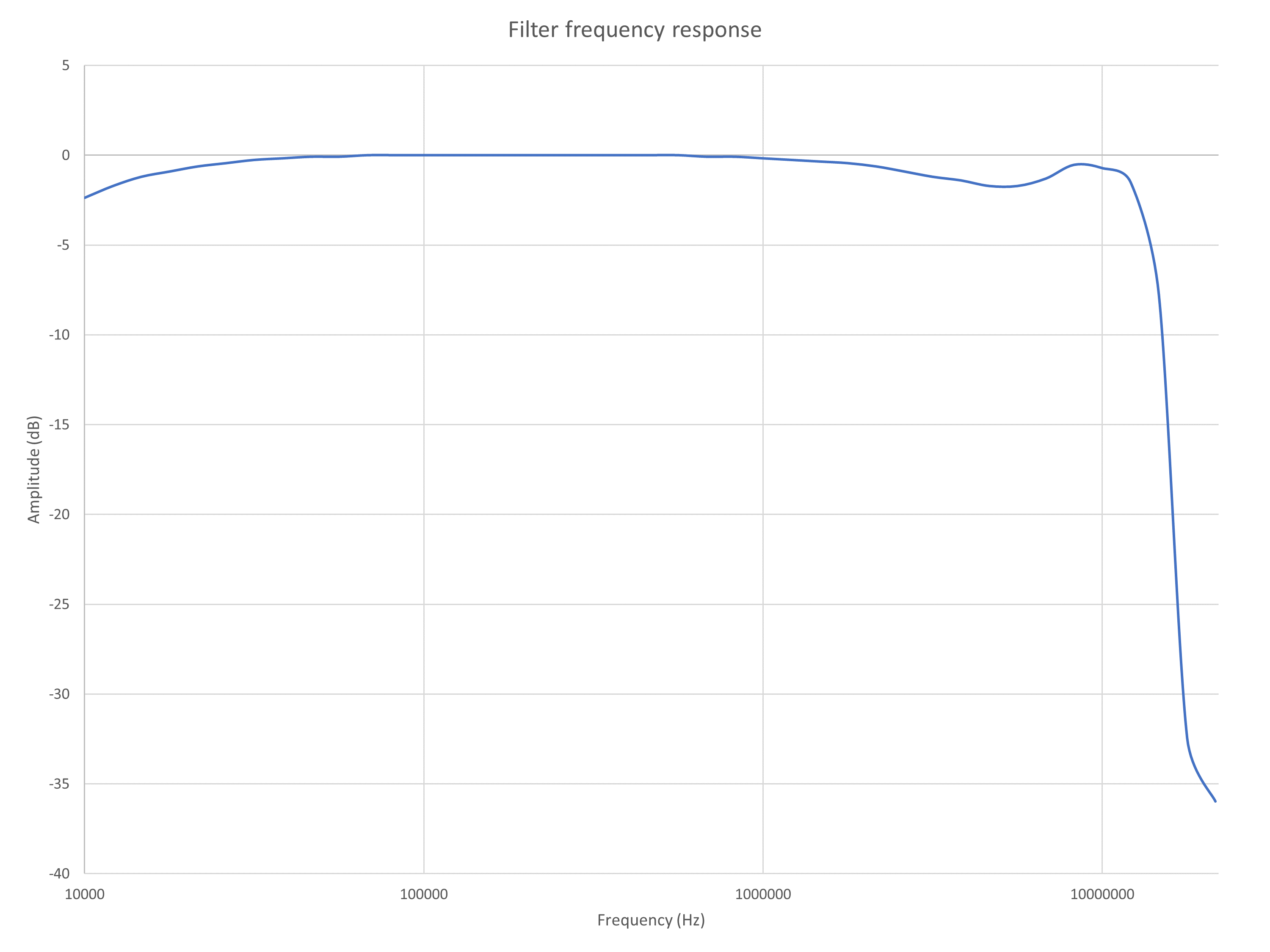
The amplification stage has a wide bandwidth and amplifies the whole RF signal with linear gain up to (and over the 100 MHz) range. In order for this signal to be digitized it's important that all frequencies above the Nyquist are removed before the ADC stage. Nyquist theorem states that the highest frequency that can be sampled is half the total sampling rate; therefore, with a 40 MSPS ADC, the highest allowed frequency is 20 MHz. An issue with the ADC process is that any frequencies present in the sampled signal above the Nyquist are 'reflected' into the sample distorting the signal and these 'aliases' of the signal cannot be removed once the sampling is complete. Therefore it is important to remove as much of the unwanted frequencies as possible in the analogue stage. To remove unwanted high-frequencies a low-pass filter (often referred to as an anti-alias filter) is employed. The filter is placed after the amplification stage to prevent additional noise since the signal amplitude is greater versus relative noise (i.e. it has a better signal to noise ratio). A passive filter design is used as it generally causes less distortion, but at the cost of signal attenuation. LaserDisc players often employ a filter which has a stop-band of 13.2 MHz (above the upper parts of the video signal) and this design is also used by the Duplicator. There are many different types of passive LPF filter designs available, however the filter used is a 2 pole elliptic D low-pass filter. Elliptic filters are desirable as they provide a very steep attenuation of the signal in the stop-band however, this is at the cost of 'ripple' in the pass-band. For the purpose of the filter design the pass-band should attenuate the signal less than -3dB. In the stop-band, attenuation should be as great as possible. The filter used by the Domesday Duplicator was designed using a filter design tool as shown in the following screen-shot (of the predicted frequency response as well as phase): [caption id="attachment_2281" align="alignnone" width="800"]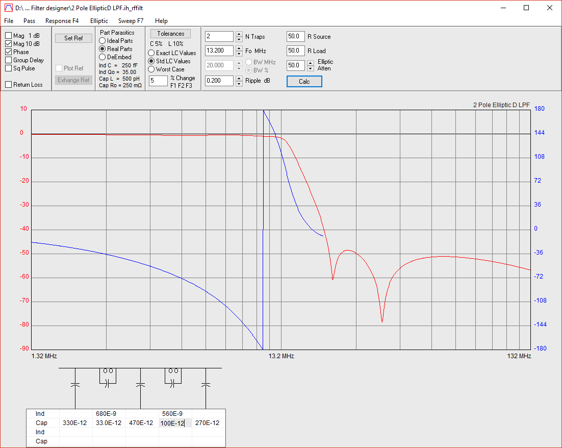
The Analogue to Digital Converter accepts the incoming RF signal from the RF Amplifier stage and converts the analogue signal into a digital sample at a rate of 40 million samples per second (MSPS). The ADC schematic is shown in the following diagram: [caption id="attachment_2240" align="alignnone" width="800"]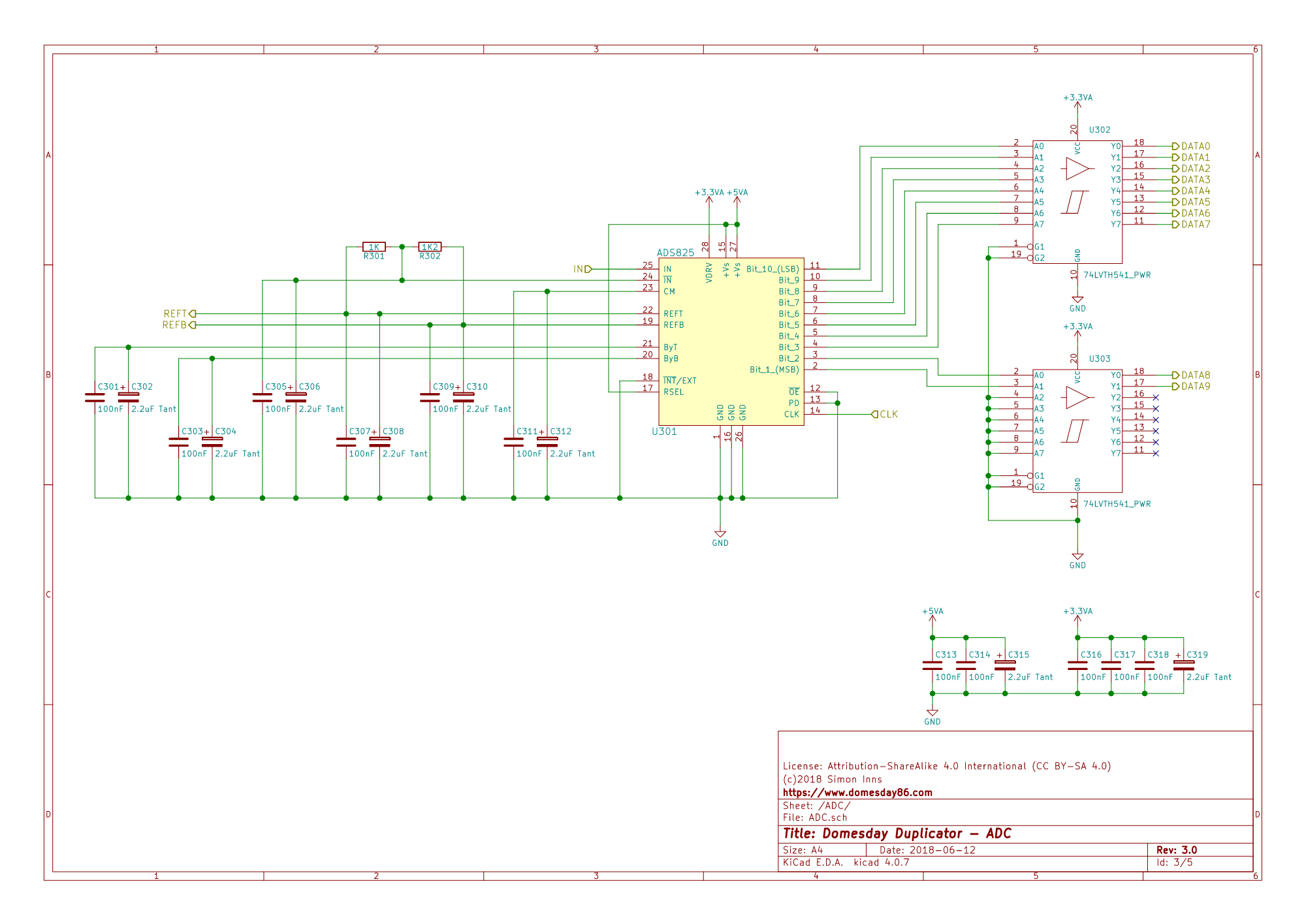
Due to the unpredictable performance of a USB 3.0 interface, an FPGA is used to act as a FIFO buffer between the ADC and the USB hardware. Although a modern PC can handle many times the bandwidth required by the application, the bandwidth is not guaranteed (since a general purpose PC is not a real-time system, other system activities can cause the available bandwidth to vary). The FPGA is provided by a DE0-Nano. The DE0-Nano is a low-cost FPGA development board from Terasic containing an Intel (Altera) Cyclone IV FPGA. The interconnection between the Domesday Duplicator and the FPGA development board is shown in the main schematic diagram above. The FPGA uses a PLL function (Phase Locked Loop) to provide a 40MHz sampling clock to the ADC as well as a communication clock to the FX3. Both clocks are generated from the DE0-Nano's on-board 50MHz clock. Data from the ADC is collected by the FPGA into a 10-bit wide dual-clock FIFO buffer. The dual-clock FIFO buffer supports separate clock rates on both the input and output of the FIFO. The interface between the FPGA and the Cypress FX3 interface is clocked at 60MHz. This dual-clock implementation allows the USB 3.0 interface to ‘catch up’ with the ADC data collection in the event of temporary loss of bandwidth. In addition the FPGA changes the 10-bit unsigned FIFO output to scaled 16-bit signed data before passing the data to the USB 3.0 interface via a 16-bit data-bus. In addition to the data-bus the FPGA provides several additional control signals used to provide flow-control of the data between the FPGA and the Cypress FX3 GPIF interface. The data bandwidth from the FPGA to the USB 3.0 interface is typically 40 million 16-bit words per second (a data transfer rate of 610 Mbits/sec) , however this can peak at 60 million words as required (a data transfer rate of 916 Mbits/sec). Note that a data transfer rate average of 610 Mbits/sec is approximately 73 Mbytes of data per second. The design provides a full 32-bit data bus between the FPGA and the FX3 and 13 control lines. Currently only 16-bits of the data-bus is used by the software (additional data bus and control signals are provided by the board to support future expansion).
The USB 3.0 interface between the FPGA and the host PC is provided by a Cypress SuperSpeed Explorer development board. This board provides a Cypress FX3 SuperSpeed USB 3.0 peripheral controller. USB 3 is required due to the data bandwidth requirement of the Domesday Duplicator (USB 2.0 only provides a realistic bandwidth of around 280Mbits/sec which is too low for the application). The FX3 provides a state-machine model (called GPIF II) that handles the transfer of data from the FPGA output data-bus to the USB 3.0 interface and can run at a maximum of 100MHz (100 million words of 32-bit data per second). For the Domesday Duplicator, the FX3 is configured to use a 16-bit data-bus and the synchronous data clock is provided by the FPGA (at 60MHz). The Cypress Superspeed Interface schematic is shown in the following diagram: [caption id="attachment_2242" align="alignnone" width="800"]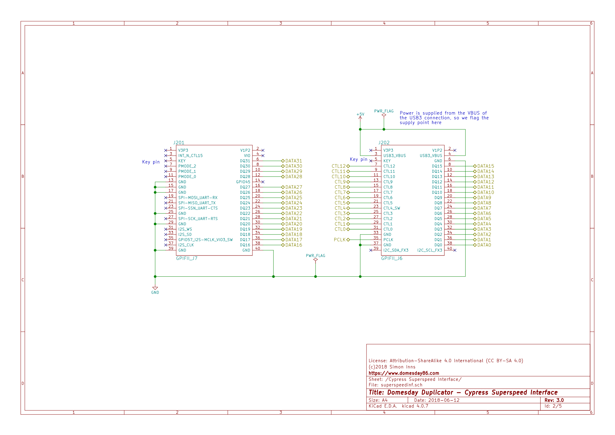
The power for the Domesday Duplicator board is sourced from the 5V supply provided by the host computer through the USB 3.0 interface on the Cypress FX3. Although the board also supplies 3.3V, there are long traces involved when routing the power from the FX3 to the Duplicator (due to the physically stacked configuration used by the design). Therefore the Duplicator provides local regulation of the 5V supply to 3.3V as well as smoothing and noise suppression of both the 3.3V and 5V supplies. The power supply schematic is shown in the following diagram: [caption id="attachment_2243" align="alignnone" width="800"]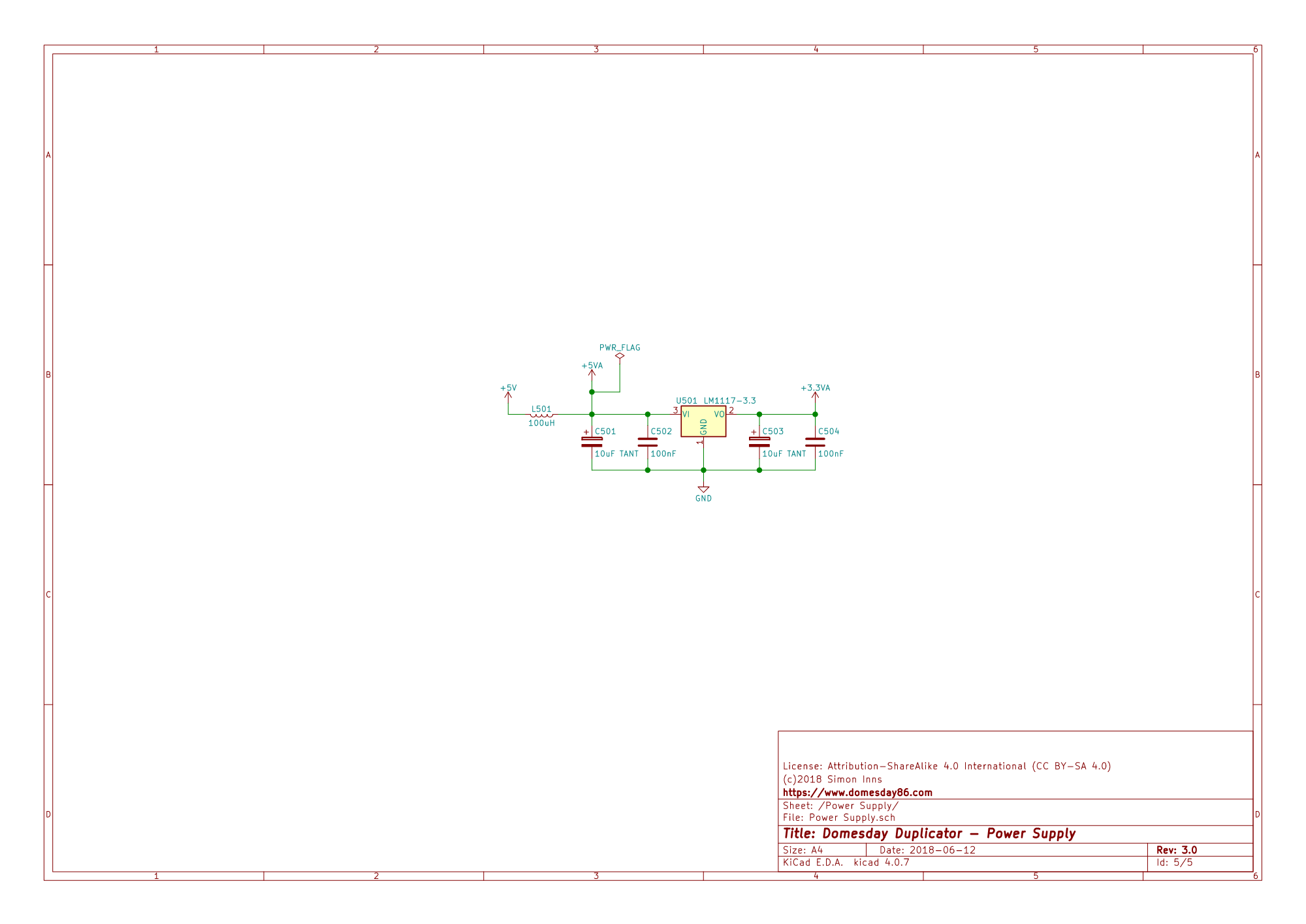
The overall layout of the Domesday Duplicator PCB can be divided in to several distinct sections namely:
- Power supply
- RF front-end
- Analogue to Digital converter
- Stacked board interconnection
These sections are illustrated by the following diagram: [caption id="attachment_2260" align="alignnone" width="800"]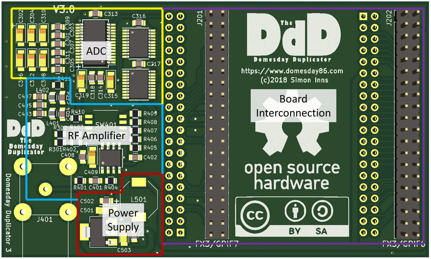
The Domesday Duplicator revision 3_0 PCB uses the following components (in order of suggested assembly sequence):
Ref
Qnty
Value
Footprint
Vendor
Article number
U301
1
ADS825E
SSOP-28 5.3x10.2mm Pitch 0.65mm
RS Components
662-0082
U302, U303
2
74LVTH541_PWR
TSSOP-20 4.4x6.5mm Pitch 0.65mm
RS Components
662-9187
U401
1
OPA690
SOIC-8 3.9x4.9mm Pitch 1.27mm
RS Components
620-0082
U501
1
LM1117-3.3
SOT-223-3
Distrelec
300-19-198
SW401
1
Gain Select DIP
Switch DIPx4 W7.62mm
Distrelec
300-90-640
C501, C503
2
10uF TANT
B_EIA-3528-21
Distrelec
300-47-865
C305, C307, C301, C303, C313, C314, C316, C317, C318, C309, C311, C401, C402, C408, C502, C504
16
100nF
0805
Distrelec
300-65-839
C302, C304, C308, C310, C315, C319, C312, C306, C409
9
2.2uF Tant
A_EIA-3216-18
RS Components
648-0660
C404
1
33pF
0805
RS Components
264-4264
C406
1
100pF
0805
RS Components
264-4292
C407
1
270pF
0805
RS Components
723-6262
C403
1
330pF
0805
RS Components
723-6271
C405
1
470pF
0805
RS Components
723-6290
R410, R411
2
47R
0805
Distrelec
300-56-808
R401
1
56R
0805
Distrelec
300-56-823
R404
1
100R
0805
Distrelec
300-56-716
R405
1
200R
0805
Distrelec
300-56-755
R409
1
560R
0805
Distrelec
300-56-819
R408
1
680R
0805
Distrelec
300-56-829
R301, R402, R403, R407
4
1K
0805
Distrelec
300-56-717
R302
1
1K2
0805
Distrelec
300-56-729
R406
1
1K5
0805
Distrelec
300-56-740
L401
1
680nH
0805
RS Components
775-4726
L402
1
560nH
0805
RS Components
786-7087
L501
1
100uH
Bourns SRN8040 Series SMD
RS Components
743-5197
J101
1
DE0-Nano_GPIO1
Pin Header Straight 2×20 Pitch 2.54mm (female)
Distrelec
300-24-958
J102
1
DE0-Nano_GPIO0
Pin Header Straight 2×20 Pitch 2.54mm (female)
Distrelec
300-24-958
J201
1
GPIFII_J7
Pin Header Straight 2×20 Pitch 2.54mm
Distrelec
143-70-334
J202
1
GPIFII_J6
Pin Header Straight 2×20 Pitch 2.54mm
Distrelec
143-70-334
J401
1
BNC_Rosenberger
BNC Socket – Rosenberger 51K204-400A5
Distrelec
146-44-967
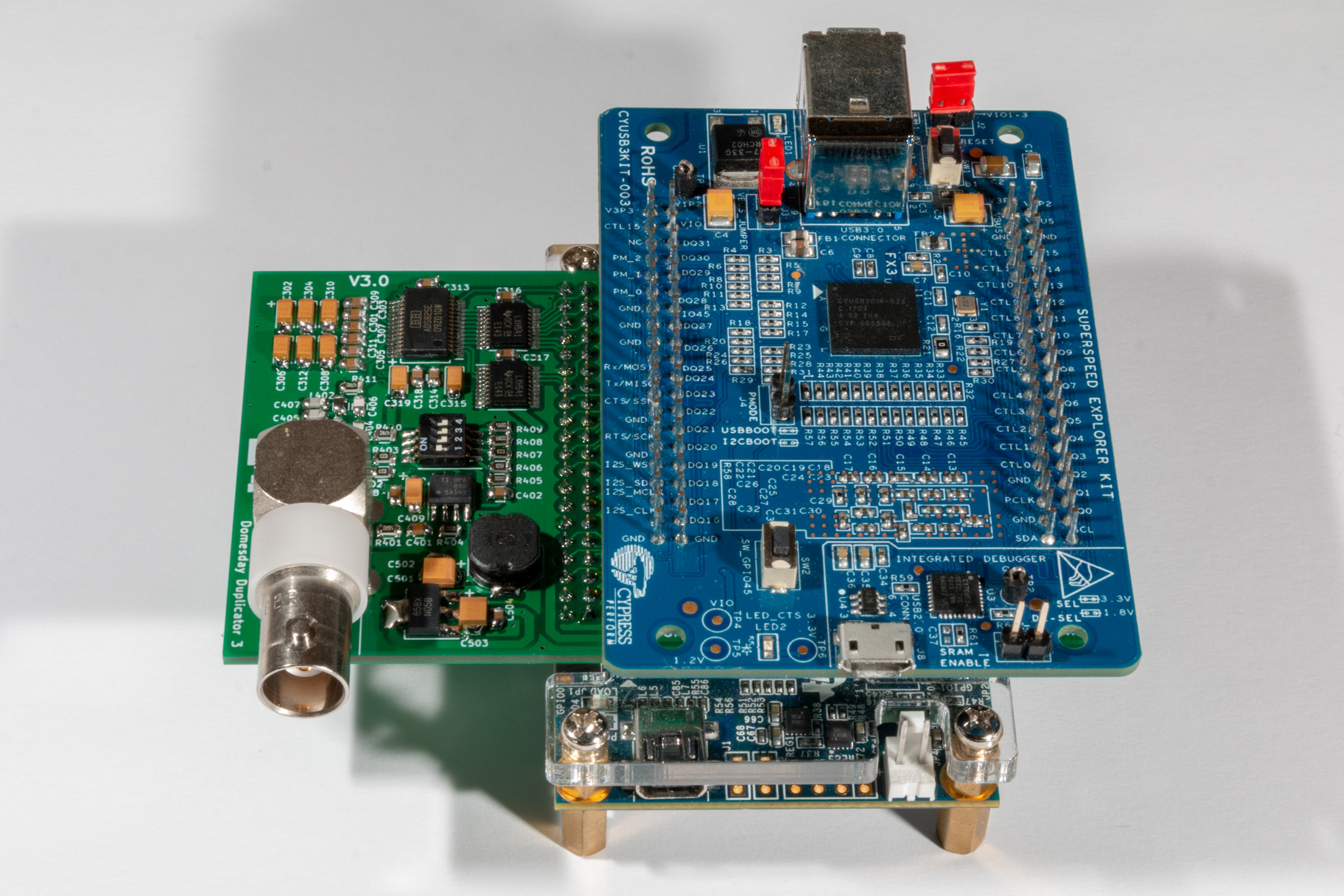
Step 1: Mount the active components and the DIP switch on the top-side of the board (U301, U302, U303, U401, U501 and SW401). Note the orientation of the integrated circuits and DIP switch; pin 1 is highlighted with a red dot: 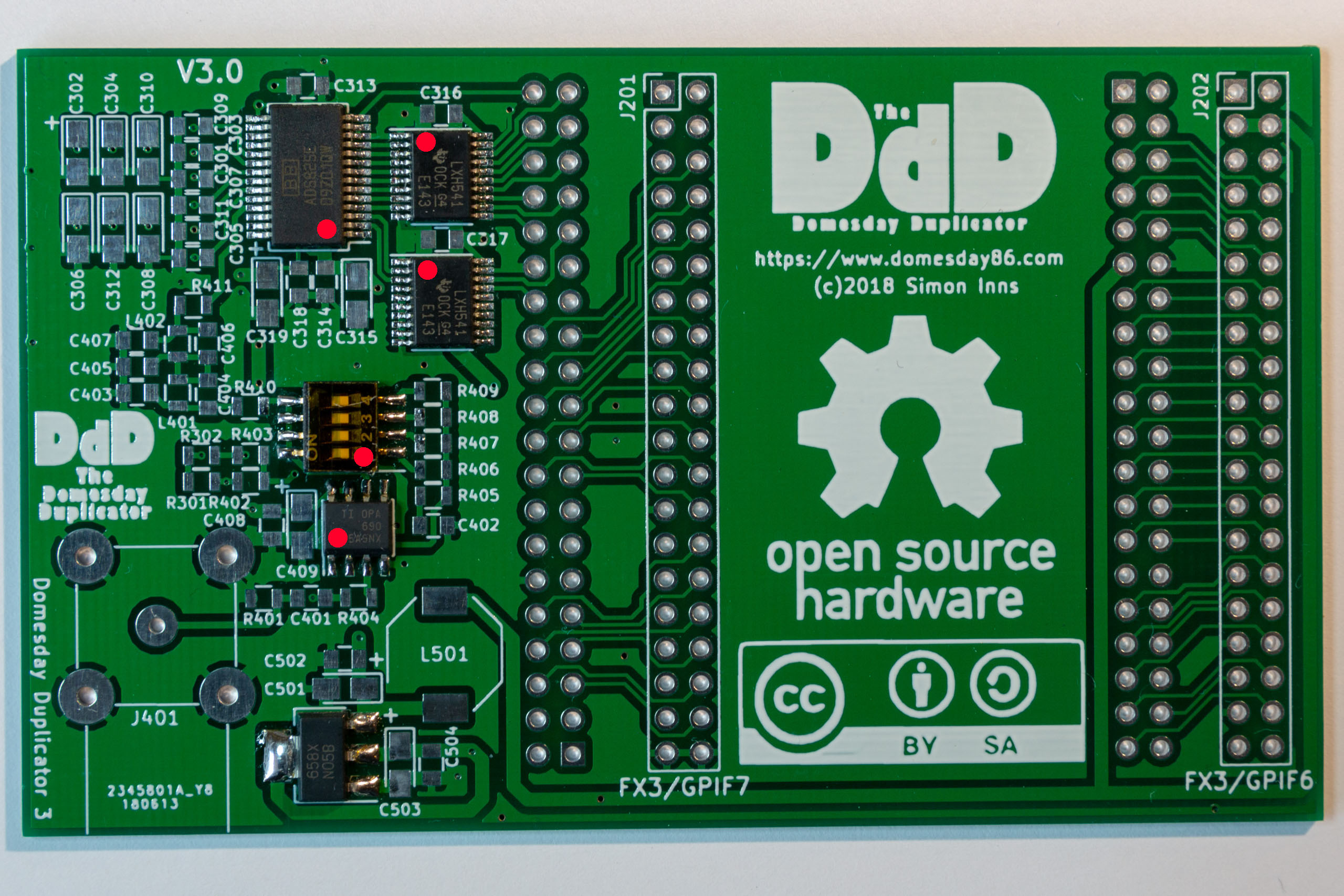
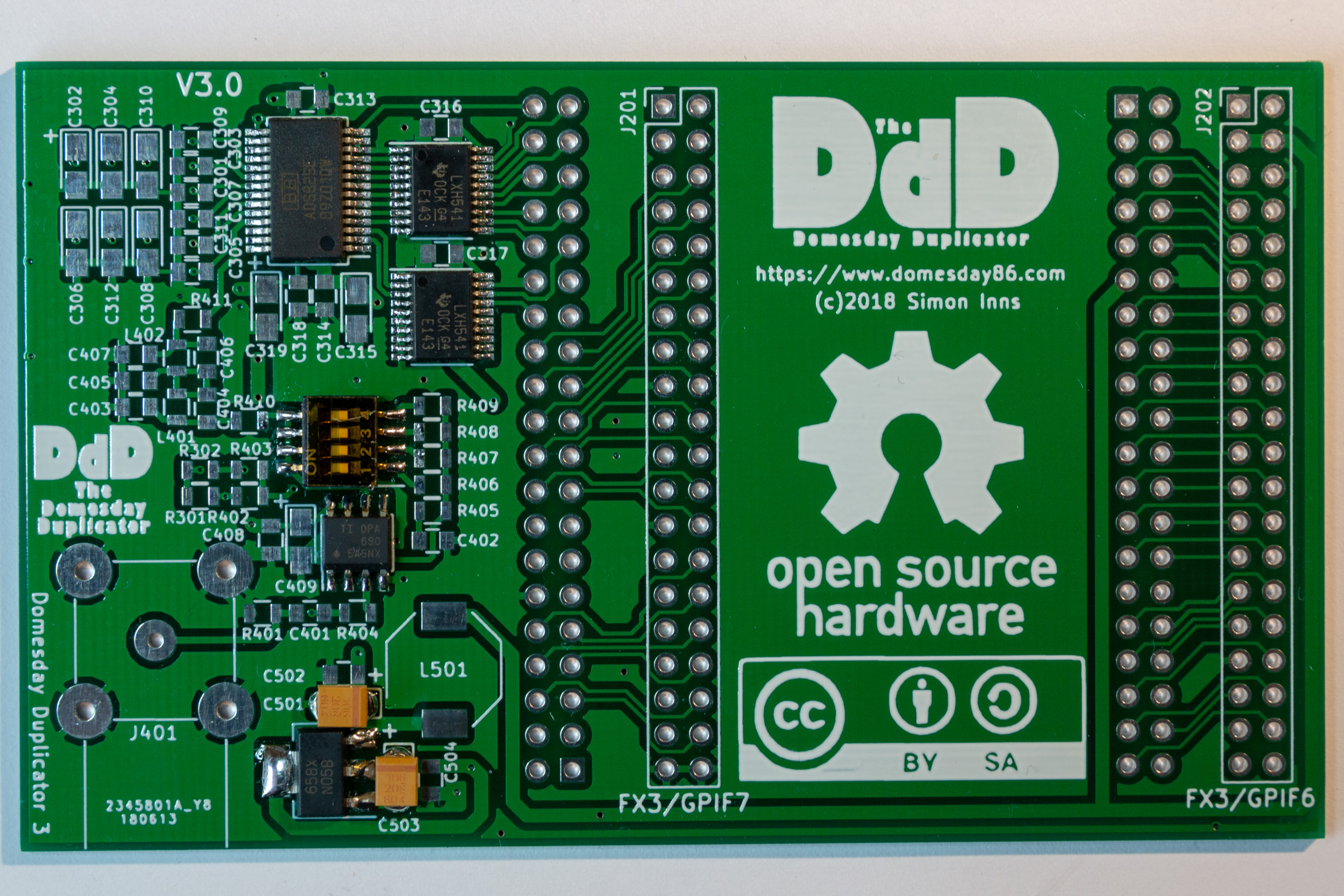
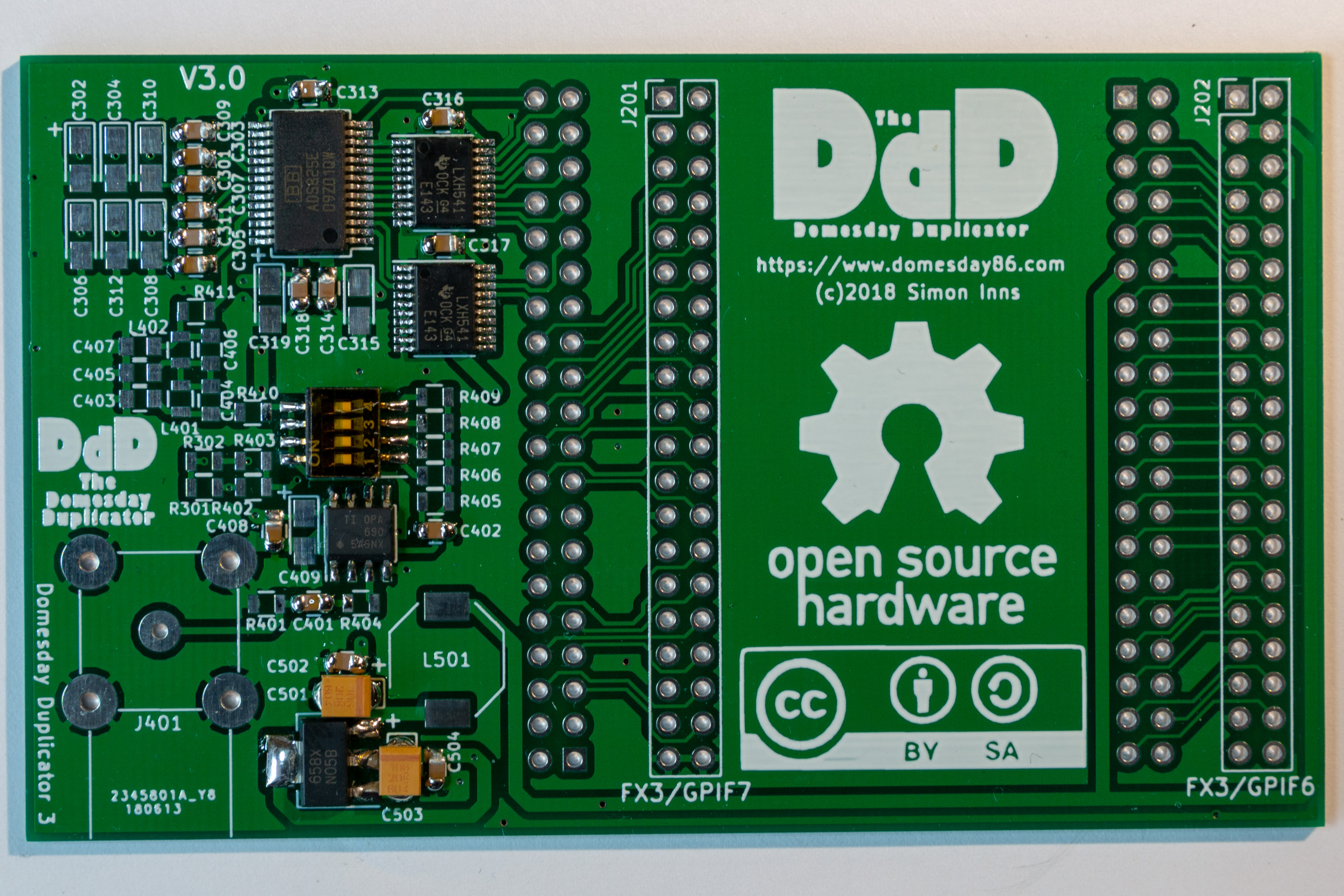
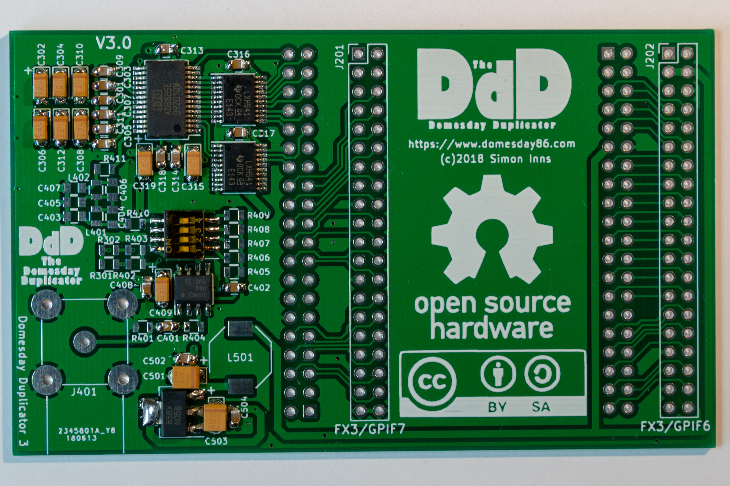
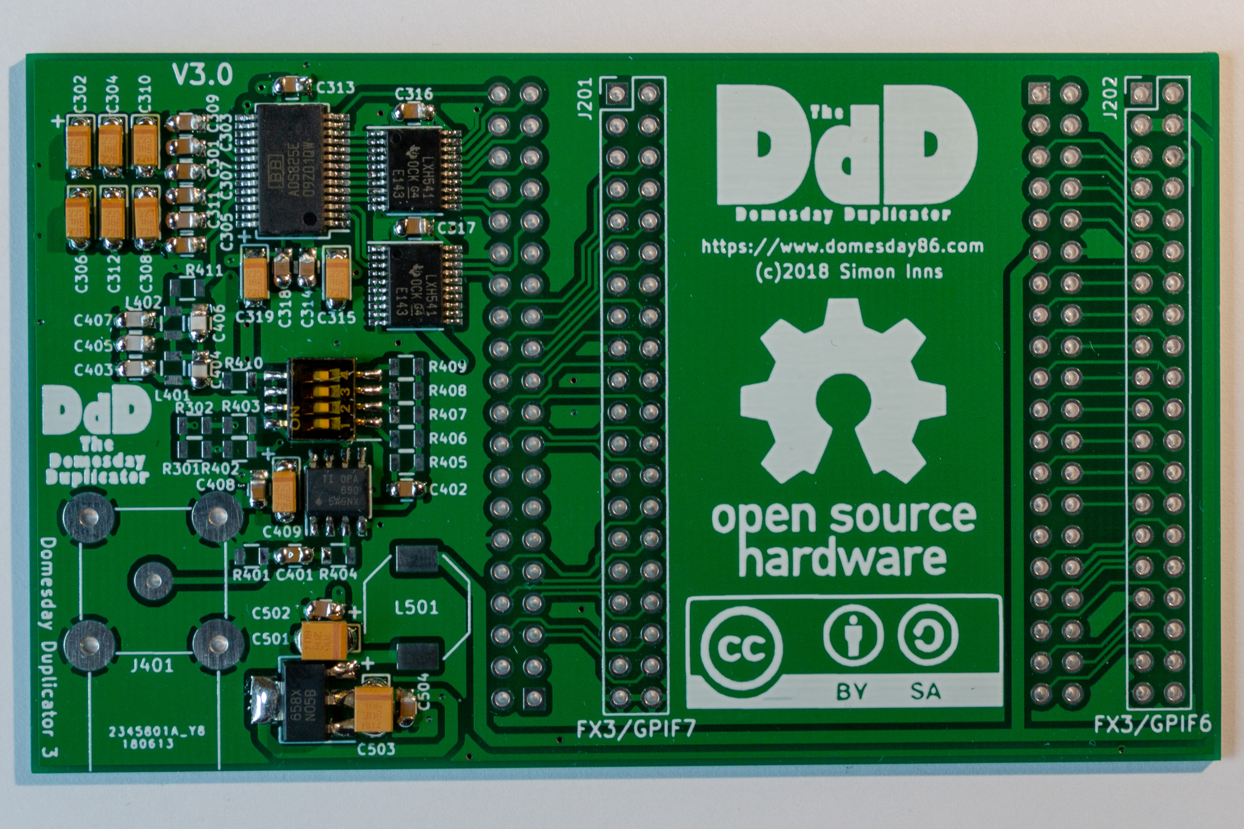
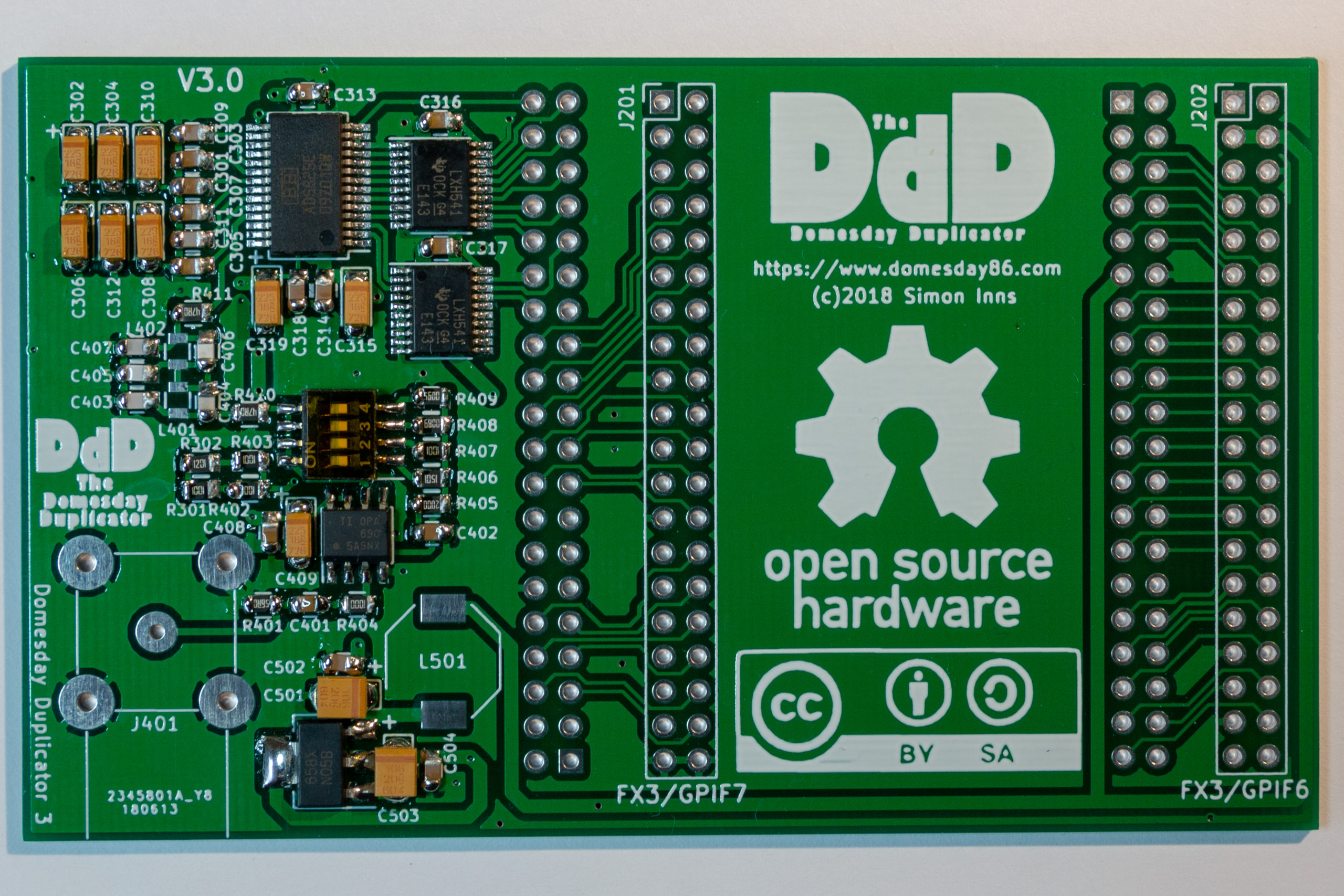
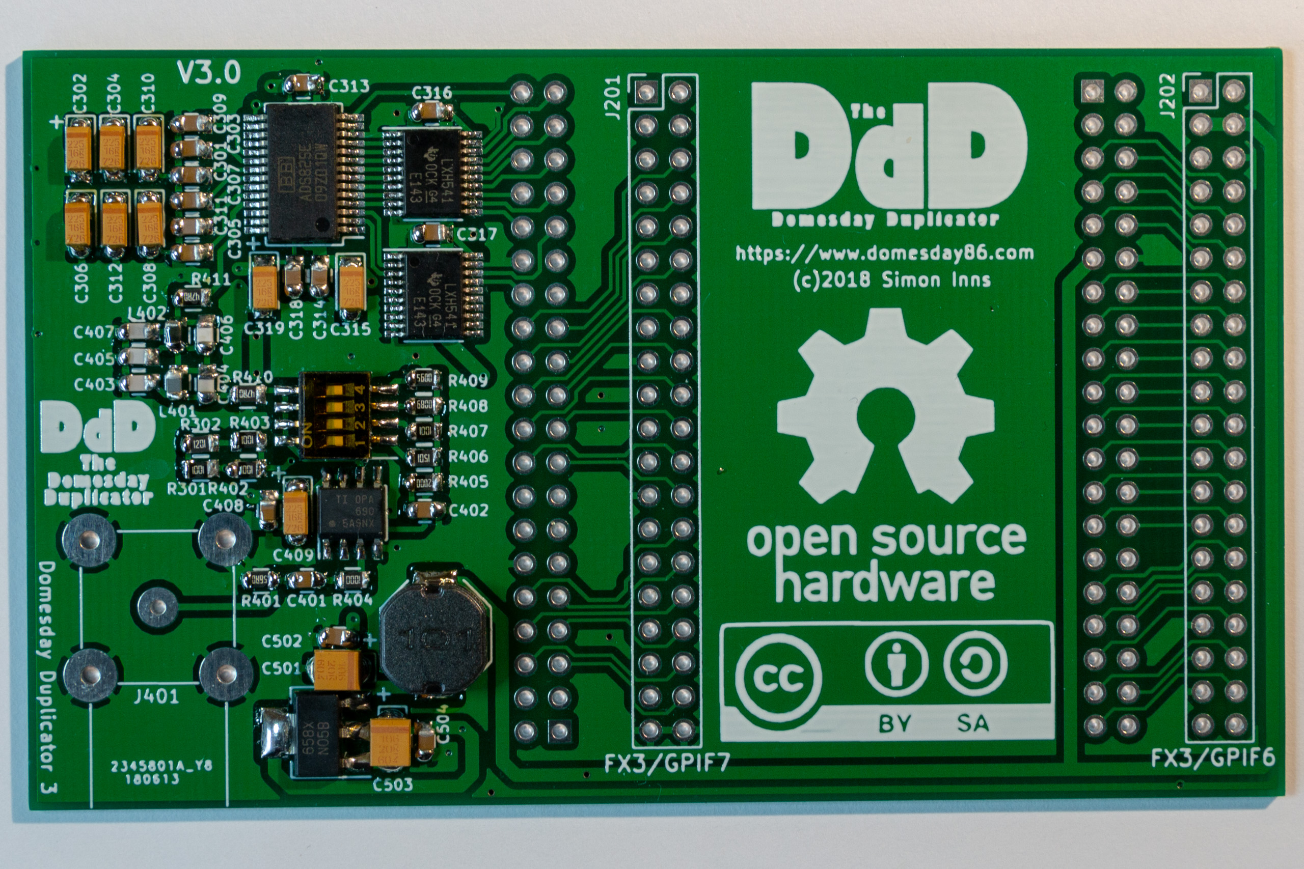
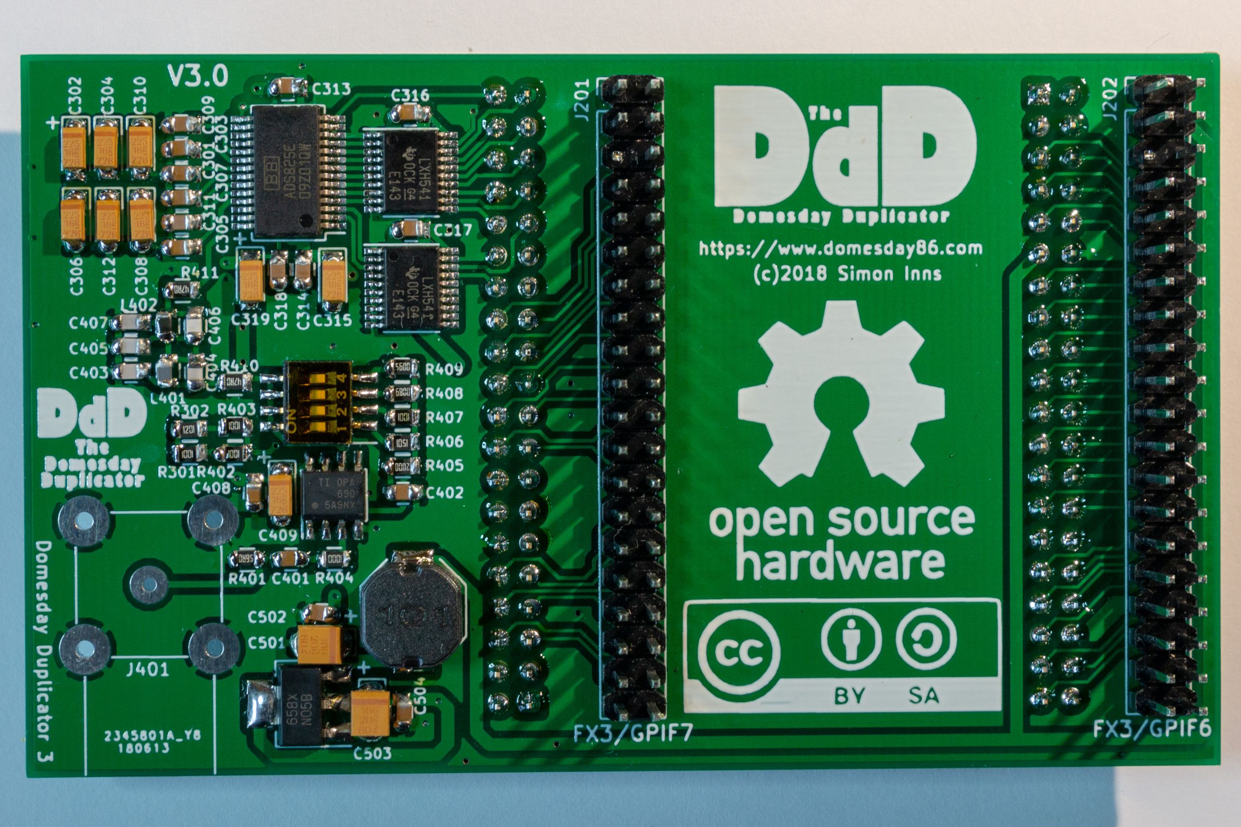
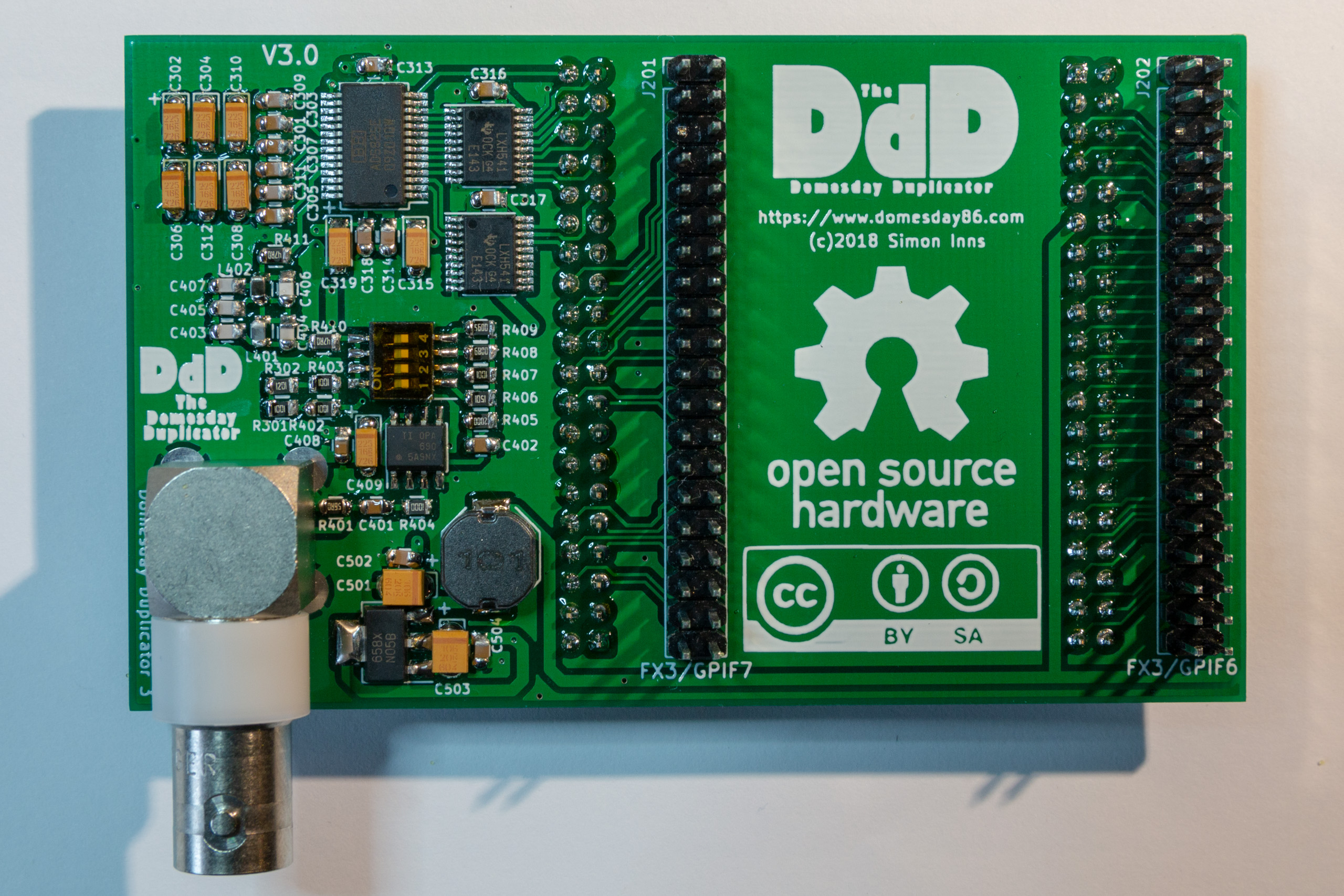
The Domesday Duplicator is designed to work with a 50 Ohm impedance source (such as the RF output from a Pioneer LD-V4300D LaserDisc player). The BNC connector on the duplicator is rated for 50 Ohms and a 50 Ohm BNC cable should be used to connect the player to the board. To prevent unwanted noise this cable should be as short as practically possible (i.e. 1m). Note that the input is not video, therefore 75 Ohm video cables should not be used.
Due to the design of the duplicator a DC-offset must be applied to the incoming RF signal before the op-amp stage of the RF front-end. This is necessary as the op-amp operates in a range of 0V-5V requiring the offset to be as close to 2.5Vs as possible (in order to provide the maximum range and sensitivity of the ADC). The ADC also requires the same DC offset on the not IN pin when acting in a single-ended configuration. This set-up provides efficient use of external components however, since the DC offset is generated separately for the op-amp and ADC there is slight variance in the offset that can cause the sampled signal to be slightly shifted (due to the accuracy of the resistors used). To compensate for the majority of the DC offset variance the revision 3_0 board contains two additional resistors (R301 and R302) that provide the reference offset to the ADC. These resistors must be matched with the DC offset of the op-amp output – therefore an asymmetrical voltage divider is used (i.e. the values of R301 and R302 are not the same). The level of variance in the DC offset will vary slightly from board-to-board (due to the 1% tolerance of the resistors). The following data shows a typical variance of a board:
- Voltage at ADC IN pin: 2.480V
- Voltage at ADC !IN pin: 2.509V
- Total variance: -0.029V (-29mV)