By Derrick Yu and Alex Liu
ECE-251 Professor Marano
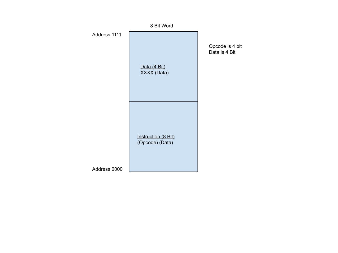
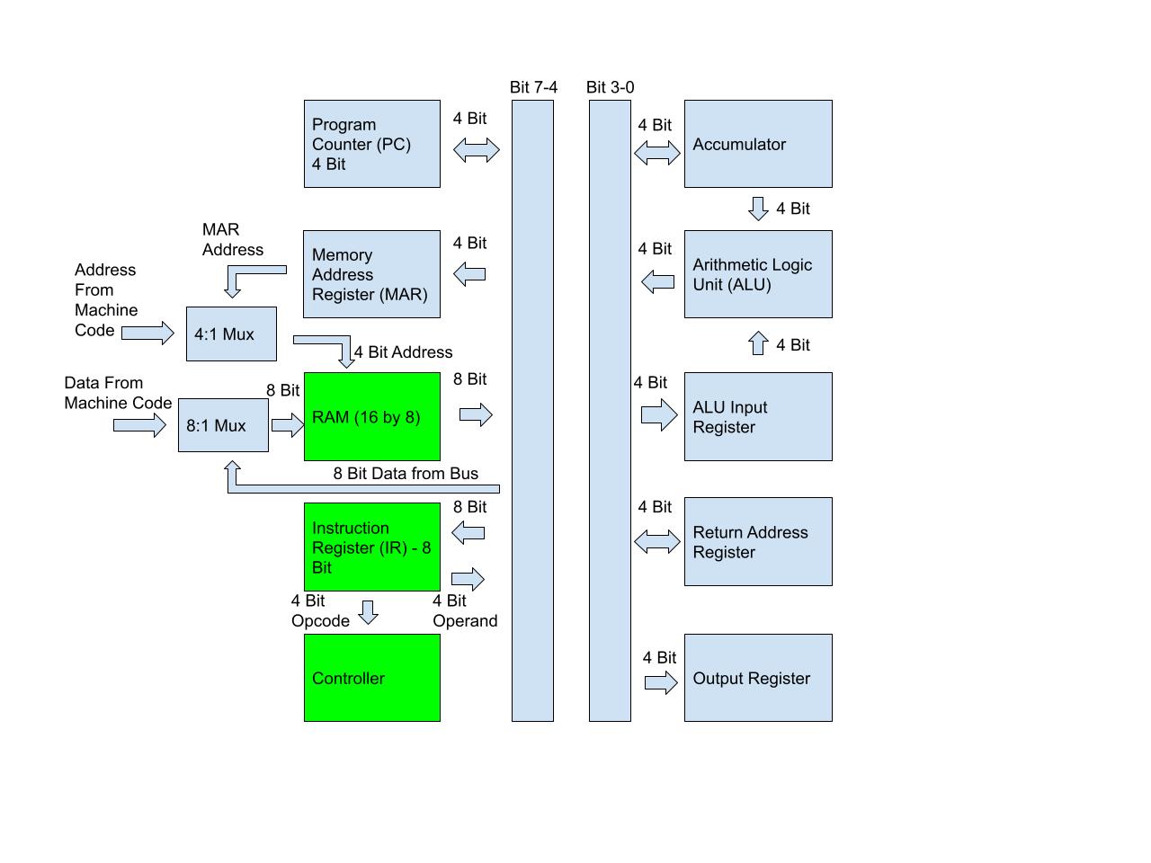
A 4-bit CPU and a 16 by 8 RAM in a von Neumann computer architecture were designed using Verilog. The CPU was modeled after the SAP computer series taught in Digital Computer Electronics by Malvino and Brown. However, this CPU has a different overall instruction set from all architectures because of its limited but useful 4 bit opcodes and the Verilog simulation had to be designed from scratch. The priority was for the CPU to be capable of doing arithmetic/logical operations, load/store, unconditional jump, and unconditional/conditional branch and link. These operations are highlighted in the ultimate Fibonacci code that will be presented later. Despite being a 4 bit CPU with the ALU operand being 4 bits, all instructions (and as a result RAM word width) are 8 bits (upper nibble is the opcode and lower nibble is the operand), therefore requiring an 8 bit data bus.
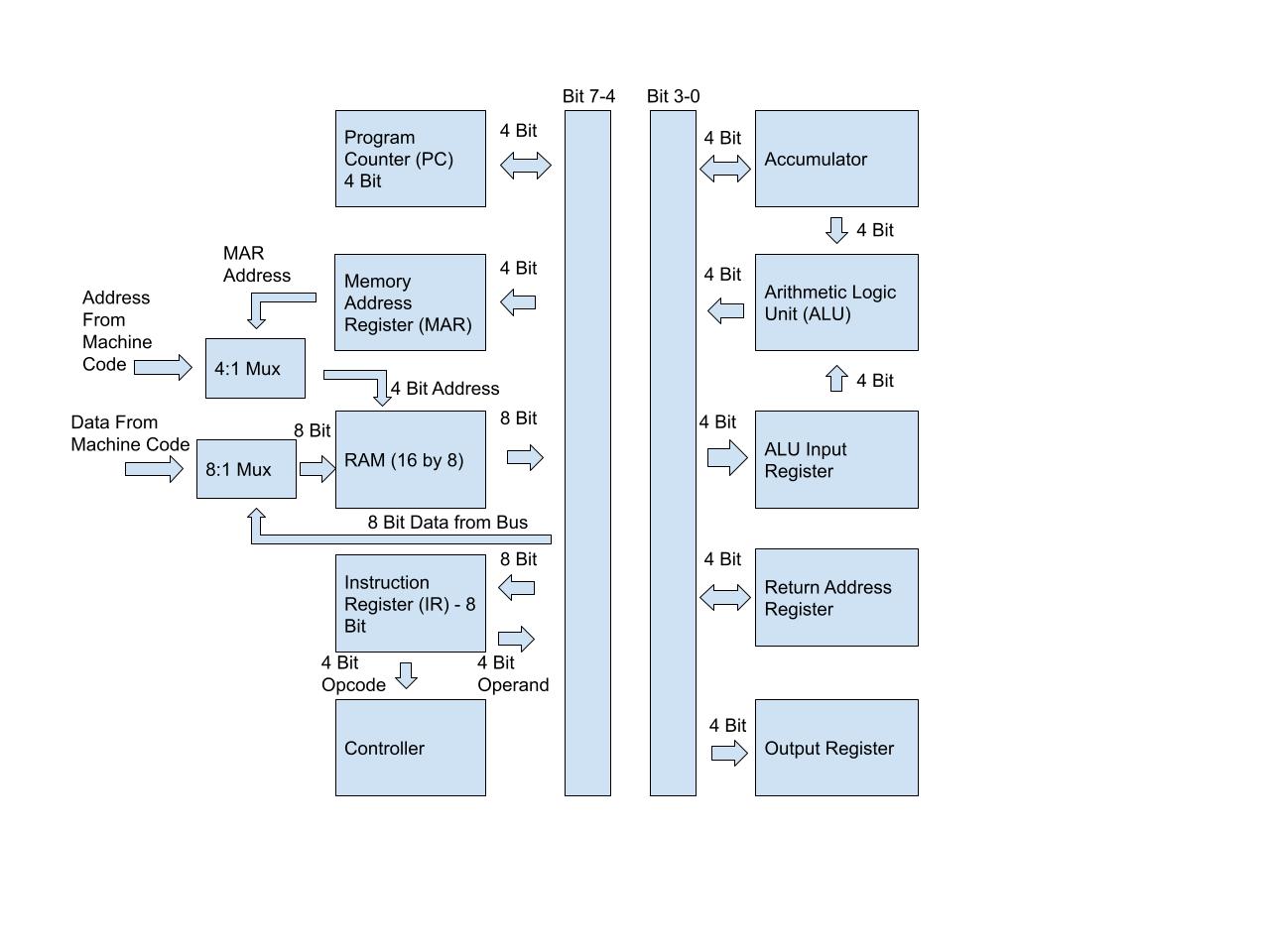
- Program Counter: Register that holds the address of the next instruction in memory. It is positive edge triggered with three control pins
- Lp - Load content from the bus into the program counter
- Cp - Increment the program counter
- Ep - Output the content of the program counter onto the bus
- Memory Address Register (MAR): Register that holds the address of the current instruction. It is positive edge triggered with two control pins
- Lm - Load content from the bus into the memory address register
- Em - Output the content of the memory address register onto the bus
- RAM: Stores data and instructions. It is positive edge triggered with two control pins
- We - Controls whether you are reading or writing to the RAM module at a certain address
- CS - Output the content of the RAM module onto the bus in READ mode
- Instruction Register: Register that holds the instruction. It is positive edge triggered with two control pins
- Li - Load the content from the bus into the instruction register
- Ei - Output the content of the instruction register onto the bus
- Controller: It decodes the opcode from the instruction and controls all control pins of all modules. It is negative edge triggered.
- Accumulator: Register that stores the result of an ALU operation. It is positive edge triggered with two control pins
- La - Load content from the bus into the accumulator
- Ea - Output the content of the accumulator onto the bus
- ALU: Performs arithmetic and logical operations. It has three control pins grouped as a single “Select” control
- ALU Select (M2 M1 M0)
- ALU Input Register: Register that holds the data that will be used to perform an operation by the ALU with the content in the accumulator. It is positive edge triggered with one control pin
- Lib - Load content from the bus into the ALU input register
- Return Address Register: Register that holds the address of the instruction that the program will return to after branching. It is positive edge triggered with two control pins
- Lc - Load content from the bus into the return address register
- Ec - Output the content of the return address register onto the bus
- Output Register: Register that holds the content that the user wants to be outputted from the accumulator. It is positive edge triggered with one control pin
- Lo - Load content from the bus into the output register
| Instruction Name | Addressing | Opcode | Format |
|---|---|---|---|
| ADD | Direct | 0000 | ADD (Address) |
| SUB | Direct | 0001 | SUB (Address) |
| MUL | Direct | 0010 | MUL (Address) |
| DIV | Direct | 0011 | DIV (Address) |
| NOT | Direct | 0100 | NOT (Address) |
| AND | Direct | 0101 | AND (Address) |
| OR | Direct | 0110 | OR (Address) |
| STOP | Implied | 0111 | STOP |
| LOAD | Direct | 1000 | LOAD (Address) |
| BRLINKZ | Direct | 1001 | BRLINKZ (Address) |
| JUMP | Direct | 1010 | JUMP (Address) |
| STORE | Direct | 1011 | STORE (Address) |
| BRLINK | Direct | 1101 | BRLINK (Address) |
| OUTPUT | Implied | 1110 | OUTPUT |
| BRR | Implied | 1111 | BRR |
Direct Addresing
| Opcode | Address |
|---|---|
| Bit 7 - 4 | Bit 3 - 0 |
Implied Addressing
| Opcode | XXXX |
|---|---|
| Bit 7 - 4 | Bit 3 - 0 |
- ADD - Add the data stored in the address (operand) in the RAM module to the data in the accumulator and load the result into the accumulator.
- SUB - Subtract the data stored in the address (operand) in the RAM module to the data in the accumulator and load the result into the accumulator.
- MUL - Multiply the data stored in the address (operand) in the RAM module to the data in the accumulator and load the result into the accumulator.
- DIV - Divide the data stored in the address (operand) in the RAM module to the data in the accumulator and load the result into the accumulator.
- NOT - Bit NOT the data stored in the address (operand) in the RAM module with the data in the accumulator and load the result into the accumulator.
- AND - Bit AND the data stored in the address (operand) in the RAM module with the data in the accumulator and load the result into the accumulator.
- OR - Bit OR the data stored in the address (operand) in the RAM module with the data in the accumulator and load the result into the accumulator.
- STOP - Stop the clock.
- LOAD - Load the data stored in the address (operand) inside the RAM module into the accumulator.
- BRLINKZ - If the zero flag of the ALU is 1, branch to a procedure that has the address stored in the operand of the instruction and load the return address (address of previous instruction + 1) into the return address register.
- JUMP - Jump to an instruction to the address stored in the operand of the instruction.
- STORE - Store the data in the accumulator to the address in the operand of the instruction.
- BRLINK - Branch to a procedure that has the address stored in the operand of the instruction and load the return address (address of previous instruction + 1) into the return address register.
- OUTPUT - Load the data stored in the accumulator into the output register.
- BRR - Return to the address in the return address register by loading the return address into the program counter.
As you can see, the majority of the instructions have a direct addressing mode. This means that the assembly code will be in terms of ADDRESSES in the RAM module, not registers like more advanced architectures. For example, the instruction “ADD 15”, means “add whatever is in address 15 in your RAM to whatever is in the accumulator”. If the number 5 is in address 15, running “ADD 15” will add 5 to the accumulator. When you program your own code, you have the freedom of adding any constant that you like, but the addresses of the constants must be higher than the addresses of the instructions (NOTE THE MEMORY HIERARCHY).
In the file “cpufinal_tb.v”, there is a section called “RAM Contents - Machine Code” where you can input your machine code so that when the testbench is running, it will load your machine code into the RAM module during simulation. The format of this section mimics the RAM hardware for readability. Make sure that the addresses for each of your instructions and data are correct.
/*RAM Contents - Machine Code (Fibonacci)*/
 /*****Address*****/    /**Instruction or Data**/
reg addr0 = 4'b0000; reg [7:0] data0 = 8'b10111111; //STORE A15
reg addr1 = 4'b0001; reg [7:0] data1 = 8'b00001110; //ADD A14
reg addr2 = 4'b0010; reg [7:0] data2 = 8'b11100000; //OUTPUT
reg addr3 = 4'b0011; reg [7:0] data3 = 8'b10111101; // STORE A13
reg addr4 = 4'b0100; reg [7:0] data4 = 8'b10001101; //LOAD A13
reg addr5 = 4'b0101; reg [7:0] data5 = 8'b10111111; //STORE A15
reg addr6 = 4'b0110; reg [7:0] data6 = 8'b00001110; //ADD A14
reg addr7 = 4'b0111; reg [7:0] data7 = 8'b11100000; // OUTPUT
reg addr8 = 4'b1000; reg [7:0] data8 = 8'b10111101; // STORE A13
reg addr9 = 4'b1001; reg [7:0] data9 = 8'b10001111; //LOAD A13
reg addr10 = 4'b1010; reg [7:0] data10 = 8'b10111110; //LOAD A14
reg addr11 = 4'b1011; reg [7:0] data11 = 8'b10101100; //JUMP A12
reg addr12 = 4'b1100; reg [7:0] data12 = 8'b00000100; //Address 0100
reg addr13 = 4'b1101; reg [7:0] data13 = 8'b00000000; //Immediate 0
reg addr14 = 4'b1110; reg [7:0] data14 = 8'b00000001; //Immediate 1
reg addr15 = 4'b1111; reg [7:0] data15 = 8'b00000001; //Immediate 1
Simply input your machine code and on your terminal, enter
iverilog -o cpufinal_tb.vvp cpufinal_tb.v
vvp cpufinal_tb.vvp
In the “Overview of Architecture” section, there are multiplexers for the address input of the RAM module and the data input of the RAM module. The multiplexers select whether the address and data inputted into the RAM module are either from the machine code during programming mode or from the memory address register and bus in run mode. When you are uploading the machine code to the RAM module, the multiplexers will be set to output whatever is from the machine code for both address and the data input (in programming mode). When you are done uploading the machine code, the multiplexers will then select the memory address register for the address of the RAM module and the bus for the data input of the RAM module (now in run mode).
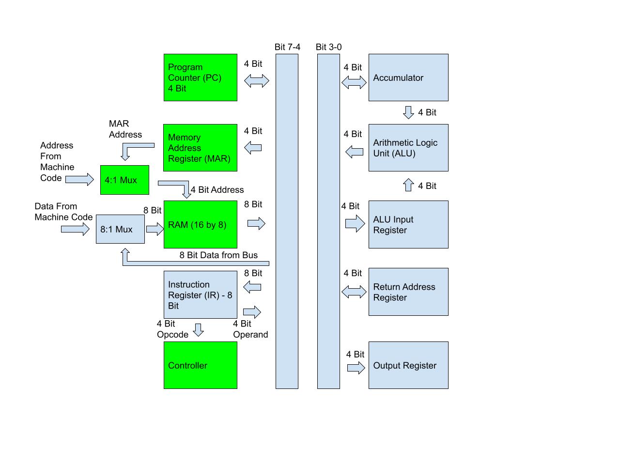
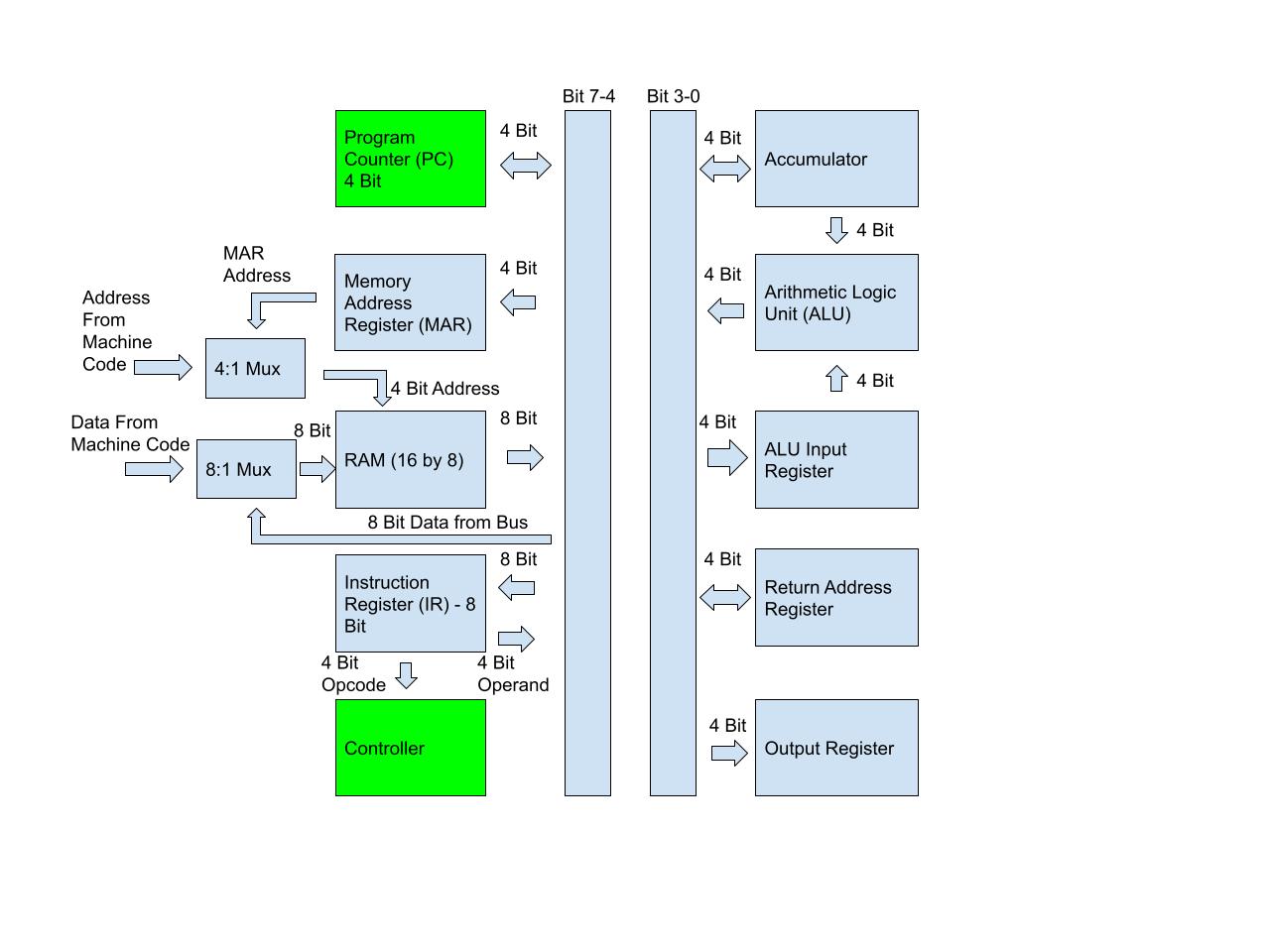
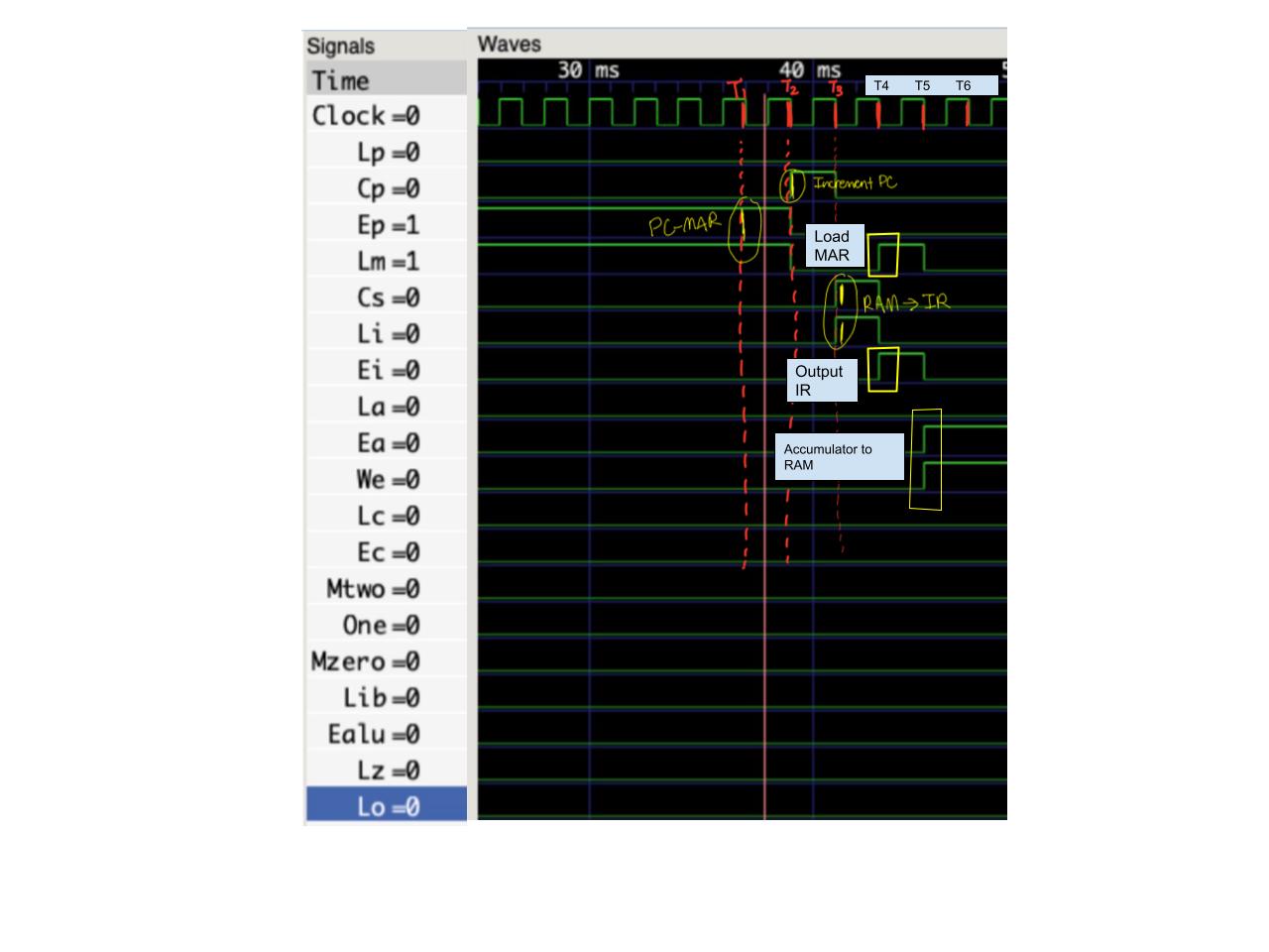
Each instruction will take six clock cycles (CPI = 6). This is because most instructions (arithmetic, BRLINKZ) will take all six clock cycles, so no operations were added to those instructions that did not need all six clock cycles to be completed. Each clock cycle has a very specific purpose in how to execute the instruction. As a result, they will be referred to as “T States” (T1-T6), where the first clock cycle is T1, the second clock cycle is T2, etc. The functionality of T1-T4 is the same for all instructions.
In the diagrams below, the "green colored" modules are the modules that are involved in the particular clock cycle.
Overall Timing Diagram:

T1:
Description: Send the content of the program counter to the memory address register, accessing the data at that address in the RAM module.
To accomplish this task, the program counter must be enabled so that it can put its content on the bus and the memory address register must have a HIGH load signal to take in content from the bus. Therefore, the Ep signal must be HIGH and the Lm load signal must be HIGH.
Diagram:
T2:
Description: Increment the Program Counter by 1.
The Cp signal is high, which causes the program counter to be incremented by 1 so that it will hold the address of the next instruction in memory.
Diagram:
T3:
Description: Send the data at the address in the RAM module to the instruction register, where it will automatically send the opcode of the instruction to the controller.
The CS signal is HIGH, allowing the RAM module to load data onto the bus. The signal Li signal is HIGH, which causes the instruction register to load in whatever data is on the bus, in this case, the data from the RAM module.
Diagram:
T4:
Description: Since all instructions are in terms of addresses, the computer will send the address operand of the instruction from the instruction register to the memory address register, setting the RAM module at the address.
The signals Ei is HIGH, which allows the instruction register to load the operand of the instruction onto the bus, The signal Lm is HIGH, which means the memory address register will load in the data on the bus, in this case, the content from the instruction register.
Diagram:
Overall Timing Diagram:
T5:
Description: The content of the accumulator will be loaded into the RAM module.
The signals Ea is HIGH, allowing the accumulator to output its content onto the bus. The signal We is HIGH, allowing the content from the bus, in this case, the accumulator, to be written into the RAM module.
Diagram:

T6:
Description: This is a no operation.
Overall Timing Diagram:
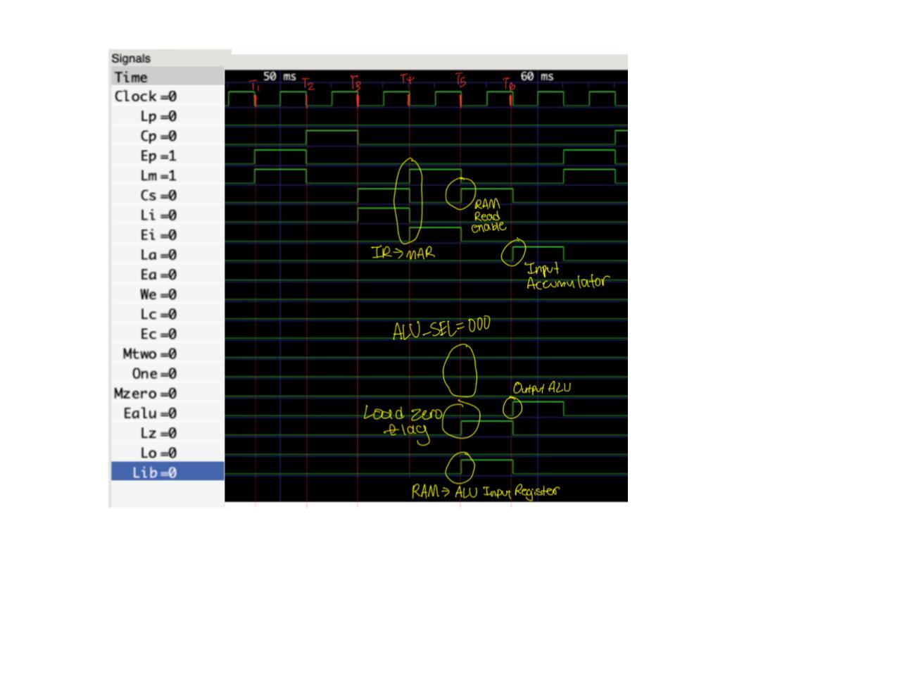
T5:
Description: The data at the address that the RAM module is set will be loaded into the ALU Input register.
The signal CS will be HIGH, allowing the RAM module to output its data onto the bus. The signal Lib will be HIGH, causing the input register to load in the data that is on the bus, in this case, the content from the RAM module.
Diagram:
T6:
Description: The ALU will load the result of the operation into the accumulator.
The signal Ealu will be HIGH, allowing the ALU to output its content onto the bus. The signal La is high, allowing the accumulator to load in the data that is on the bus, in this case, the content of the ALU. Also, the ALU Select is set at 000, which represents the ADD operation.
Diagram:
Overall Timing Diagram:
T5:
Description: The data at the address of the RAM module will be loaded into the program counter.
The signal Cs is HIGH, allowing the RAM module to load its content onto the bus. The signal Lp is HIGH, allowing the program counter to load in data from the bus, in this case, the content from the RAM module.
Diagram:
T6:
Description: This is a no operation.