2. Basic Knowledge
Disclaimer, this will likely be a poor/entry-level explanation of aspects of EE (Electrical Engineering) and other information relevant to keyboard PCB design. I recommend using other sources (e.g. Googling/YouTube) if you want proper, comprehensive explanations.
Many of the terms used throughout the guide will be explained in this section, so I recommend going over this section and educating yourself to avoid future confusion. Feel free to come back to this section if there’s some sort of term or concept you don’t understand in the middle of the guide. I may also miss a few things, so this section is definitely subject to change in the future.
In case you don't already know about the basics of electronics, I would highly advise looking through YouTube/Google for resources on learning them. Having a solid understand of electronics basics sets the foundation for what you can learn in terms of PCB design.
I would recommend at least understanding these terms before continuing:
- Circuits (open vs closed)
- Switches (what they do as an electrical component in general)
- Voltage (V), Current (I), Resistance (R)
- Resistors
- AC Power vs DC Power
Better resource: What is a Diode? | Fluke
Diodes basically allow current to only flow in one direction. They are essential to the functionality of a switch matrix (will be explained further later in this guide).
Better resource: Capacitors Explained - The basics how capacitors work working principle
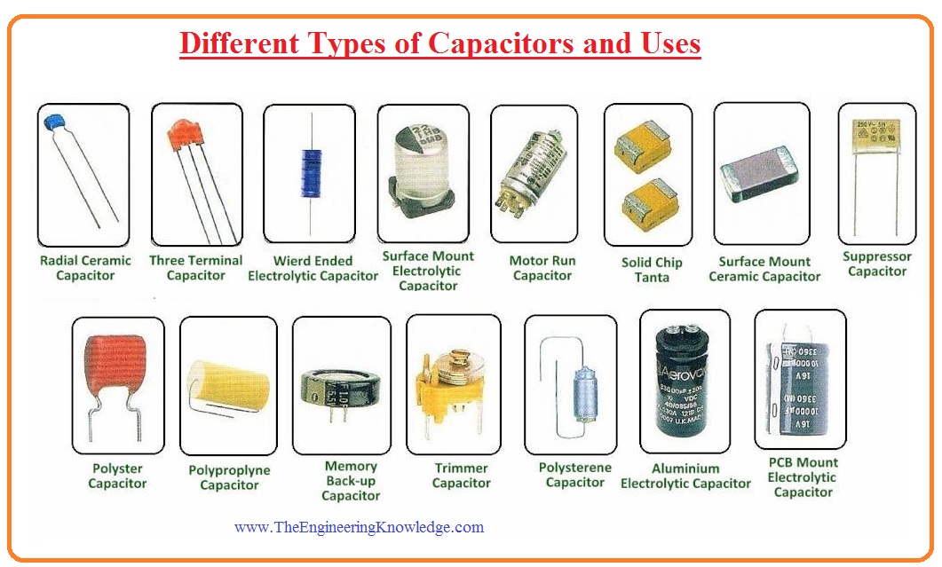
Capacitors (or ‘caps’ for short) are mainly used in keyboard PCBs to reduce noise (unwanted change of a signal/current due to electromagnetic interference, or "EMI") in a circuit.
Better resource: What is the Use of a Decoupling Capacitor?
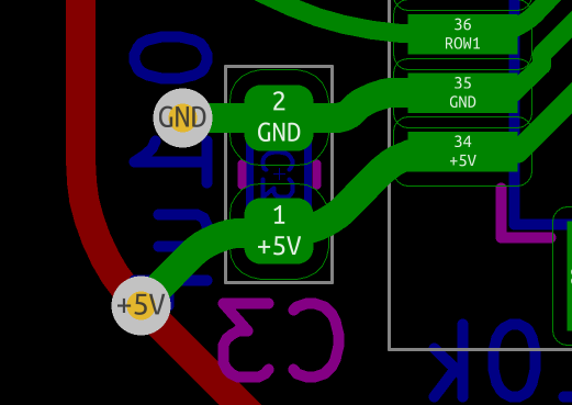
Decoupling capacitors are used to help provide ICs (integrated circuits: basically those tiny chips you see) with a steady voltage/supply of power. Micro-controllers (MCU: microcontroller unit) are an example of an IC that generally need to be applied with a steady voltage to protect the sensitive circuitry inside of them. EMI can cause noise throughout the PCB/circuit and lead to an unsteady voltage. By placing decoupling capacitors close to the controller, they can effectively cancel out noise by supplying supplementary power when the voltage drops too low and absorbing power when voltage is too high.
Note: “decoupling capacitor” is just a name given to certain capacitors with that specific role, they aren’t a special type of capacitor.
Placement and tracing of decoupling capacitors is important as to not make them useless. There is a chance that a controller may just not function if it is done wrong (though admittedly the chances are low). There are many resources online regarding decoupling capacitor placement/routing (one is linked above), but I’ll be going over how you should layout them (specifically for the controller we will be using) in this guide later on.
Example placement of a single 0.1uF (100nF) decoupling capacitor (for an ATMega32u4 2 layer keyboard PCB):
If you’re living in the 21st century, you probably know what Light Emitting Diodes (LEDs) are. They take a voltage, and emit light. They can be pretty bright for how small they are, but can also be power hungry at full brightness if used in large quantities/arrays.
RGB (red, green, blue) LEDs, e.g.
WS2812(B)LEDs, will consume more power because they actually consist of three LEDs, one for red, green and blue. They also contain a controller on-board to interpret a data signal that requires further power.
I won’t be covering how to add a per-key RGB LED switch matrix as it is out of the scope of this guide, but I may make a follow up tutorial in the future. Other resources exist online already if you want to learn how (or you can just ask people), but I wouldn’t recommend attempting it for a first PCB.
Watch these videos before I botch my explanation of PCBs (second video is pretty informative): How Do PCBs Work? / What is a PCB?
Essentially, PCBs are made of core fiberglass material (most commonly FR4) with various layers of copper in which traces connect various components together.
Vias act as pathways between layers, connecting traces and allowing them to hop from layer to layer. They are important, but should only be used when necessary. What are PCB vias?
Complex PCBs such as PC motherboards can have upwards of 14 layers, however PCBs can get as simple as just 1 layer. For keyboards, 2 layers are generally used.
The below image shows a 4 layer pcb, and how vias connect traces between the layers:

WIP:
- SMT/D and THT
- Component “form factors”
- Symbols
- Footprints
This is an optional (but interesting and informative) video on USB and how it applies to keyboards: How does a USB keyboard work?.
Modern keyboards generally operate at USB 2.0 speeds. USB (2.0) connections consist of the following four: power (+/5V/VCC), ground (-/GND) and a pair of data lines/pins:

Below is the pinout of a Micro USB connector:

Micro USB connectors used to be common a few years back, but many keyboards nowadays opt to use a USB Type-C connector. Type-C connectors have quite a few extra pins, required for hitting USB 3+ speeds, that aren’t important for USB 2.0 connection. These are the only pins on a standard Type-C connector required for a USB 2.0 keyboard:

Type-C connections running on USB 2.0 devices also require 5.1k pullup resistors between the CC pins and ground. You'll see this in the schematic for the keyboard later in the guide.
A side note: mid-mount type C connectors do exist, e.g.
TYPE-C-31-M-14.
- MCUs
- Common types/options (will expand later)
- AVR vs ARM
- Crystal oscillators
- Decoupling capacitors
- Bootloader/DFU
- Flashing headers (e.g. ISP)
- Reset circuit
- Eeprom/Flash storage
- EMI reduction
- Data traces
- ESD
- (Poly)Fuse
- Ground fills (will be expanded upon later)