This repository presents the design of 4-bit_Flash_ADC implemented using eSim open source EDA tool.
- Abstract
- Introduction
- 4-bit_Flash_ADC
- Tools Used
- Pre-Layout Schematics and Simulations
- Simulations
- Netlist
- References
- Acknowledgement
- Author
Analog to digital converter (ADC) is an integral part of communication and an important asset for virtual sign processing. Analog to digital converter (ADC), find a wide variety of applications in today’s digitalized world. Flash ADCs are quickest among all of the forms of ADCs located so far. A 4bit Analog-to-Digital Converter (ADC) is designed for low strength and low power consumption. It calls for 2N-1 comparators, an encoder to transform thermometer code to binary code. In this paper, we are going to design a 4bit flash Analog-to-Digital Converter (ADC) to gain excessive velocity the use of 130nm CMOS technology. The results received also are provided here. The physical circuit is extra compact than the preceding design. The analog output of each comparator depends upon the input, the reference voltage supplied to the priority encoder, and finally, the virtual output obtained. Power, processing time, and region are all minimized. This design may be used for modem excessive-velocity ADC applications. In this, all processes have been carried out of a CMOS-based 4bit flash Analog-to-Digital Converter (ADC) using Open-Source Software eSim, etc.
Analog to Digital Converters (ADCs) are the maximum essential devices, which connect Analog blocks with digital blocks and use everywhere all over the world. ADC is a tool that converts the input Analog amount to digital numbers. ADCs incorporate 3 fundamentals parameters, which can’t be changed once it has been planned, and the parameters consist of speed, resolution, and power dissipation. ADC, which is being mentioned nowadays, requires a structure having low energy dissipation and high velocity of operation. A single structure cannot be used for all of the packages as various varieties of ADCs range from every different on the idea of overall performance parameters inclusive of velocity, power consumption, and decision. Hence, it is extraordinarily essential to select an ADC for each specific application. A distinctive type of ADCs is available like SAR ADC, Dual-Slope ADC, Sigma-Delta ADC, and Flash ADC but amongst all these, the maximum commonly applied ADC is the Flash ADC due to its higher trade-off among its overall performance measurements. Flash ADCs are used for applications in which excessive velocity and low decisions are required. Flash ADC has a bank of comparators testing the input signal in parallel, the comparator financial institution output is fed to an encoder good judgment circuit that produces a completely unique virtual code for every voltage ranges.
The fundamental block diagram of 4-bit Flash ADC is given. It consists of three primary components: resistors, comparators, and encoders. For N-bit Flash ADC 2N resistors and 2N–1 comparator are required. For 4-bit ADC the circuit utilizes (2222)-1= 16-1=15 comparators and (2222) =16 resistors. The comparator comprises of wideband and low advantage tiers cascaded together. At excessive frequencies, the low advantage is acquired as it is difficult to acquire excessive bandwidth and excessive advantage at an equal time. Each comparator has a reference voltage that's 1 LSB better than that of the only one below it withinside the chain. An analog voltage is continued to every voltage comparator to evaluate enter voltage with regard to voltages. The reference voltage is created via way of means of the resistive stepping stool circuit and depending upon the correlation made among VIN and the comparator generates Vref, zero and 1 output. If VIN is much less than Vref, the output is 0 in any other case. The output of the comparator is fed to the concern encoder to acquire the digitalized output.
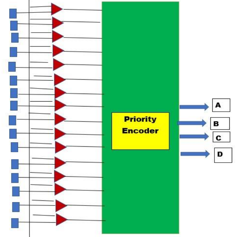
fig.1: REFERENCE CIRCUIT 4-bit_Flash_ADC
Comparator performs an important component withinside the design of Analog-to-Digital converters (ADC). The execution of the goal application is essentially impacted by the design of the comparator.
The velocity and resolution of an ADC are laid low with the enter offset voltage, delay and input signal variety of comparator. The two-level pen-loop comparator includes different stages. The first level comprises a differential amplifier and the second level includes an output advantage level as proven in Fig. 1 As this circuit incorporates a minimal quantity of transistors, its circuit area is small.
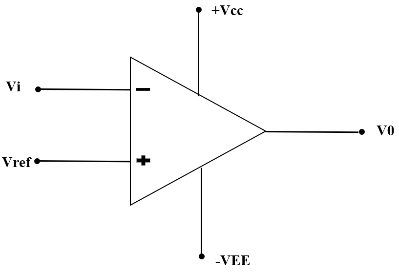
fig.2: Comparator
1). An encoder is used to reduce the quantity of a number of wires wished in a circuit.
2). It gives a coded output with the aid of using assigning a priority to the number of bits of input.
3). A priority encoder could have a couple of inputs activated at an equal time.
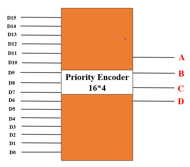
fig.3: Priority Encoder
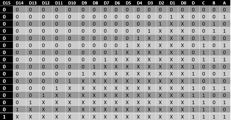
fig.4: 16x4 Priority Encoder Truth Table
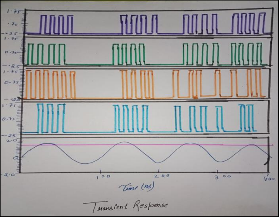
fig.5: REFERENCE WAVEFORM 4-bit_Flash_ADC
eSim is a CAD tool that helps electronic system designers to design, test and analyse their circuits. But the important feature of this tool is that it is open source and hence the user can modify the source as per his/her need. The software provides a generic, modular and extensible platform for experiment with electronic circuits. This software runs on all Ubuntu Linux distributions and some flavours of Windows. It uses Python, KiCad and Ngspice. The objective behind the development of eSim is to provide an open source EDA solution for electronics and electrical engineers. The software should be capable of performing schematic creation, PCB design and circuit simulation (analog, digital and mixed signal). It should provide facilities to create new models and components. The architecture of eSim has been designed by keeping these objectives in mind.

Fig.6: eSim open source EDA tool
Ngspice is a general purpose circuit simulation program for nonlinear dc, nonlinear transient, and linear ac analysis. Circuits may contain resistors, capacitors, inductors, mutual inductors, independent voltage and current sources, four types of dependent sources, lossless and lossy transmission lines (two separate implementations), switches, uniform distributed RC lines, and the five most common semiconductor devices: diodes, BJTs, JFETs, MESFETs, and MOSFET.
Makerchip Circuit design has been a game for big industry for far too long! Makerchip provides free and instant access to the latest tools from your browser and from your desktop. This includes open-source tools and proprietary ones. Turning the tables for the open-source community, Redwood EDA, LLC's commercial capabilities are often available for open-source development here first--before they are available commercially!

Fig.7: Makerchip
• Verilog:
Verilog is a Hardware Description Language; a textual format for describing electronic circuits and systems. Applied to electronic design, Verilog is intended to be used
for verification through simulation, for timing analysis, for test analysis (testability analysis and fault grading) and for logic synthesis
Verilator: It is a tool which converts Verilog code to C++ objects.
module balakrishna_priority_encoder(out,i);
  output reg [3:0]out;
  input [15:0]i;
 always @ (*)
   casex(i)
     	16'b0000000000000001:out = 4'b0000;
		16'b000000000000001x:out = 4'b0001;
		16'b00000000000001xx:out = 4'b0010;
		16'b0000000000001xxx:out = 4'b0011;
		16'b000000000001xxxx:out = 4'b0100;
		16'b00000000001xxxxx:out = 4'b0101;
		16'b0000000001xxxxxx:out = 4'b0110;
		16'b00000001xxxxxxxx:out = 4'b0111;
		16'b0000001xxxxxxxxx:out = 4'b1000;
		16'b000001xxxxxxxxxx:out = 4'b1001;
		16'b00001xxxxxxxxxxx:out = 4'b1010;
		16'b0001xxxxxxxxxxxx:out = 4'b1011;
		16'b001xxxxxxxxxxxxx:out = 4'b1100;
		16'b001xxxxxxxxxxxxx:out = 4'b1101;
		16'b001xxxxxxxxxxxxx:out = 4'b1110;
		16'b1xxxxxxxxxxxxxxx:out = 4'b1111;
default : out=4'bxxxx;
   endcase
endmodule
verilog code of 16x4 priority encoder in makerchip IDE
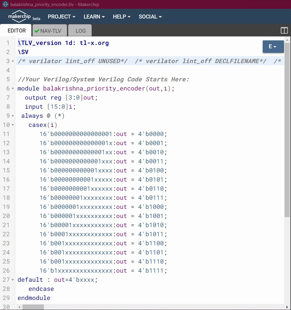
Fig.8.1:
Simulation of 16x4 priority encoder in makerchip IDE
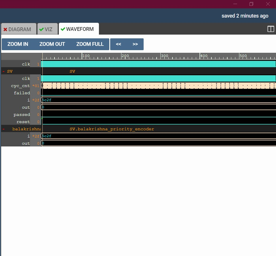
Fig.8.2:
Simulation of verilog code when any random value is taken
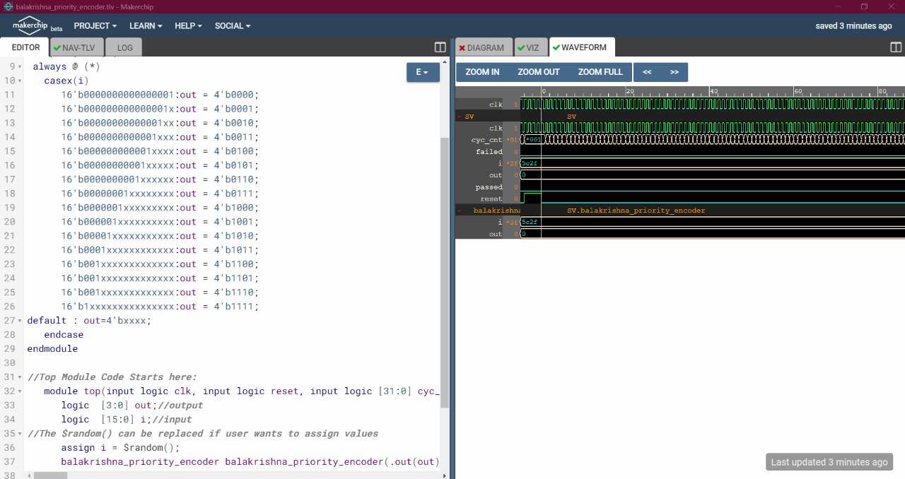
Fig.8.3:
Simulation of verilog code when user has given the value
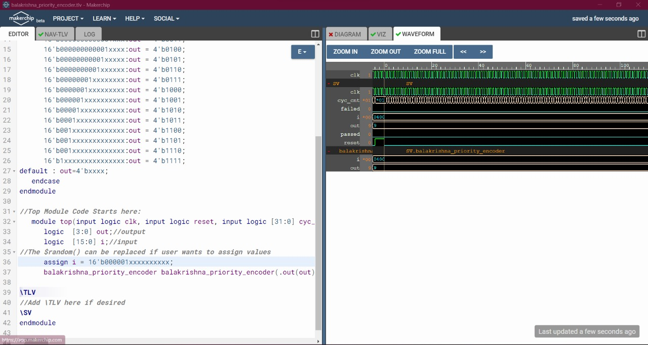
Fig.8.4:
Comparator is a significant circuit in analog and mixed signal design. As we know that operational amplifier can be used as a multipurpose device so here we have used Opamp that is lm_741 as a comparator that is OPAMP as a COMPARATOR. The planned schematic of comparator circuit. Here, we used the non-inverting comparator so, the sine signal is applied as the input signal on the high-quality terminal or non-inverting terminal of the opamp while the reference voltage (Vref) is given on the other terminal or inverting terminal of the opamp.

Fig.9: Comparator Circuit
This is the schematic circuit of 16x4 Priority Encoder which consist of a priority encoder i.e.,(balakrishna_priority_encoder) , with 2 adc bridge is used , one dac bridge is used and 4 resistors with respect to the input applied as pulse signal at the output and forplotting the waveform plot is used also labels are used for labelling the inputs and outputs of priority encoder.

Fig.10: 16x4 Priority encoder circuit
Flash analog–to–digital Converter schematic diagram. Flash ADC is N-bit Flash ADC in which there are 2N resistors and 2N–1 comparator are required. For 4-bit ADC the circuit utilizes (2x2x2x2)-1= 16-1=15 comparators that is from 0 to 15 and (2x2x2x2) =16 resistors. The input voltage for each of the comparators is larger than the reference voltage for the comparators which is applied on the other terminal. Each comparator produces a "1", which means that when its analog input voltage (Vin) is greater than the reference voltage (Vref) which is applied to it or else, the comparator output is "0". The Flash ADC consists of three primary components: a ladder of resistor network which is connected in series with each other, comparators, and Priority encoder. The analog input voltage is at the identical terminal as compared to the reference voltage degrees generated from resistors string and the speed of A/D conversion is consequently maximized. The outputs of comparators look like a binary code(BC) that's a combination of a sequence of zeros and a sequence of ones, e.g., 0000…0011…1111. Since binary code is generally desired for digital signal processing, a thermometer code is then altered to a binary code encoder. Optimizations on area rate, circuit latencies and electricity intake are very much projected. In this, we've low electricity Comparator used withinside the implementation all through a Comparator Circuit & implementation Specification.
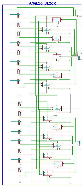
Fig.11: Analog Block circuit
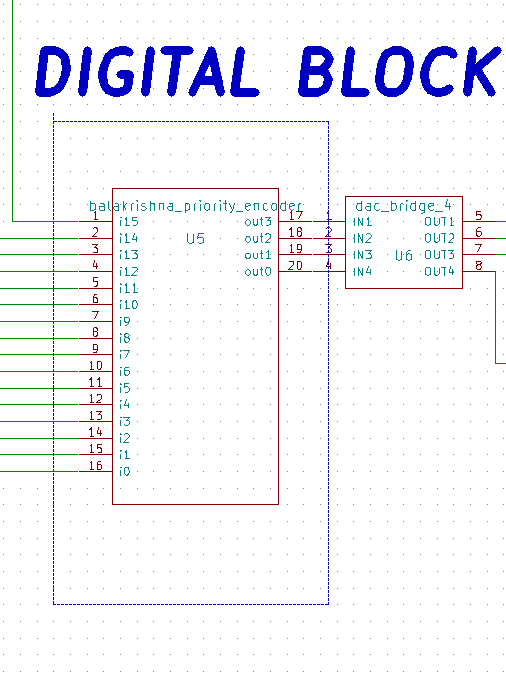
Fig.12: Digital Block circuit
This is the mixed signal schematic of 4 bit FLASH ADC which includes two major blocks i.e., Analog Block and Digital Block . As we know that mixed signal circuit are the mixture of analog as well as digital circuits.
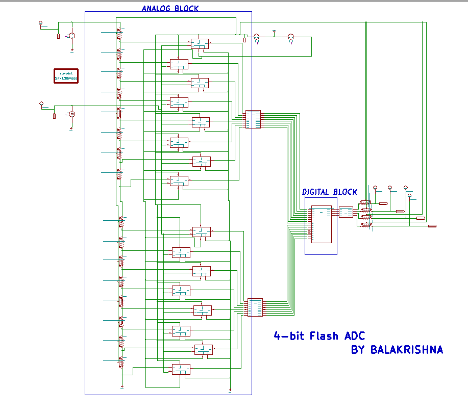
Fig.13.1: Mixed Signal circuit

Fig.14: 16x4 Priority encoder Waveform(1)
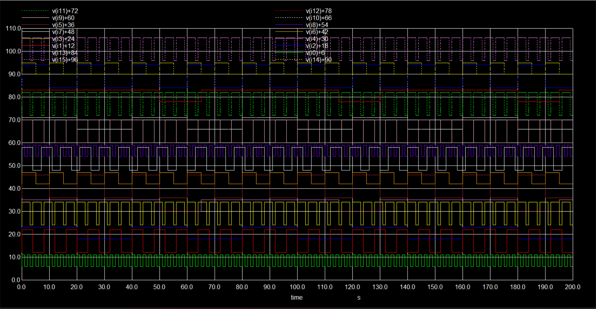
Fig.15: 16x4 Priority encoder Waveform(2)

Fig.16: comparator waveform
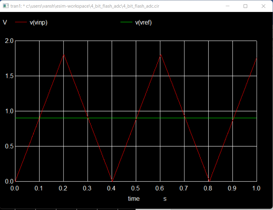
Fig.19.1: 4-bit_flash_adc_waveform(1)
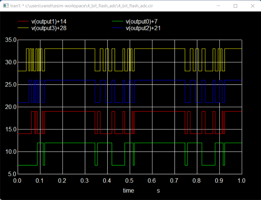
Fig.19.2: 4-bit_flash_adc_waveform(2)
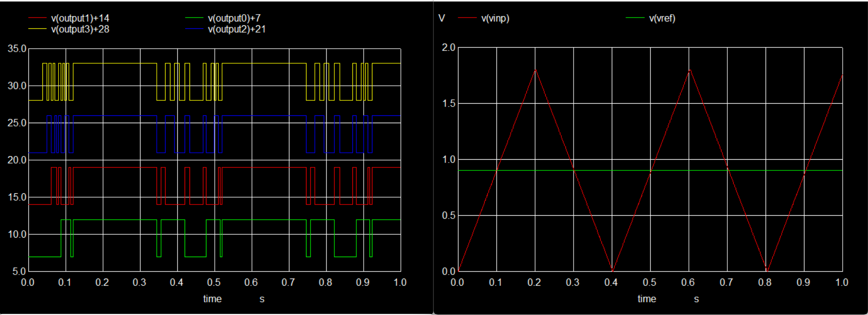
Fig.19.3: 4-bit_flash_adc_waveform(3)
[1]. Refer to the netlist of the circuit here: Netlist_of_comparator
[2]. Refer to the netlist of the circuit here: Netlist _of _16x4 _Priority_encoder
[3]. Refer to the netlist of the circuit here: Netlist_4-bit_Flash_ADC
- Open eSim
- Run NgVeri-Makerchip
- Add top level verilog file in Makerchip Tab
- Click on NgVeri tab
- Add dependency files
- Click on Run Verilog to NgSpice Converter
- Debug if any errors
- Model created successfully
- Open a new terminal
- Clone this project using the following command:
https://github.com/BALAKRISHNA-EPPILI/4-bit_flash-ADC-Using-sky130nm.git - Change directory:
cd eSim_4_bit_flash_adc - Run ngspice:
ngspice 4_bit_flash_adc.cir.out - To run the project in eSim:
- Run eSim
- Load the project
- Open eeSchema
[1]. https://www.ripublication.com/ijems_spl/ijemsv8n1_05.pdf
[2]. https://research.ijcaonline.org/volume61/number11/pxc3884802.pdf
[3]. https://ijeat.org/wpcontent/uploads/papers/v2i2/B0932112212.pdf
- eSim
- Indian Institute Of Technology (IIT) Bombay
- Kunal Ghosh, Founder, VSD Corp. Pvt. Ltd
- VLSI System Design (VSD) Corp. Pvt. Ltd India
- SUMANTO KAR
• E Balakrishna, B.Tech(ECE), Dronacharya Group of Institutions, Greater Nodia, Uttar Pradesh.