2.5D, 3D and 3.5D Package or integration technology refers to advanced packaging techniques used in the semiconductor industry. These technologies enable the integration of multiple components or dies into a single package, resulting in increased functionality and performance.
In 3D or 3.5D packaging, multiple dies are stacked vertically, interconnected using through-silicon vias (TSVs) or microbumps. This vertical integration allows for shorter interconnect lengths, reduced power consumption, and improved thermal management. 2.5D and 3D packaging is commonly used in applications such as high-performance computing, graphics processing units (GPUs), and memory modules.
On the other hand, 2.5D packaging involves the integration of multiple dies on a silicon interposer. The interposer acts as a bridge, providing electrical connections between the dies. This technology allows for the combination of different types of dies, such as processors, memory, and sensors, in a single package. 2.5D packaging offers improved performance, power efficiency, and system miniaturization.
Both 3D and 2.5D package technologies have revolutionized the semiconductor industry by enabling the development of smaller, faster, and more power-efficient electronic devices. These packaging techniques play a crucial role in the advancement of various fields, including mobile devices, automotive electronics, and data centers.
This repository will provide a comprehensive and detailed introduction to the technology behind 3D and 2.5D packaging. It will cover various aspects such as the principles, applications, and advancements in this field. Additionally, it will explore the benefits and challenges associated with these technologies.This comprehensive guide aims to equip designers with the knowledge and insights needed to navigate the exciting world of 2.5 D, 3D and 3.5D package technology.
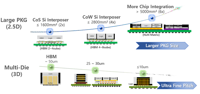
(Source: TechSearch International)
While traditional packaging divides the silicon wafer into individual chips first and then attaches the chips to the PCB and establishes the electrical connections, wafer-level packaging creates the electrical connections and molds at the wafer level, and then divides the chips using a laser. The main difference between wafer-level chip-scale packaging (WLCSP) and flip chips in terms of chip configuration is that WLCSPs do not have a substrate between the die and the PCB. Instead, redistribution layers (RDLs) are used as a replacement for the substrate, resulting in a smaller package size and improved thermal conduction.
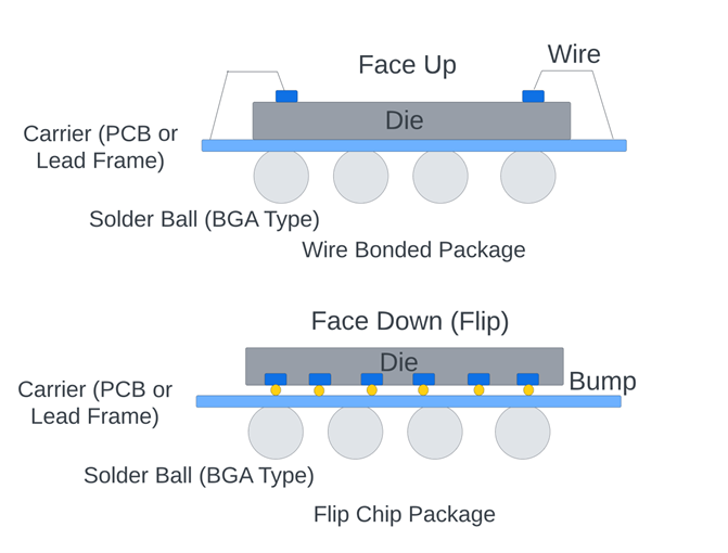
Flip chip, also known as controlled collapse chip connection or its abbreviation, C4,[1] is a method for interconnecting dies such as semiconductor devices, IC chips, integrated passive devices and microelectromechanical systems (MEMS), to external circuitry with solder bumps that have been deposited onto the chip pads.
The solder bumps are deposited on the chip pads on the top side of the wafer during the final wafer processing step. In order to mount the chip to external circuitry (e.g., a circuit board or another chip or wafer), it is flipped over so that its top side faces down, and aligned so that its pads align with matching pads on the external circuit, and then the solder is reflowed to complete the interconnect. This is in contrast to wire bonding, in which the chip is mounted upright and fine wires are welded onto the chip pads and lead frame contacts to interconnect the chip pads to external circuitry.(Source:Wiki)
Flip-chip packaging is the most common and lowest-cost technology currently in use, mainly for central processing units, smartphones, and radio-frequency system-in-package solutions.
Process steps:
Integrated circuits are created on the wafer.
Pads are metallized on the surface of the chips.
A solder ball is deposited on each of the pads, in a process called wafer bumping
Chips are cut.
Chips are flipped and positioned so that the solder balls are facing the connectors on the external circuitry.
Solder balls are then remelted (typically using hot air reflow).
Mounted chip is "underfilled" using a (capillary, shown here) electrically-insulating adhesive.
(Source: anysilicon)
Wafer-level packaging is categorized into two types: fan-in and fan-out.
In fan-in wafer-level packaging, which is primarily utilized for low-end mobile phones that necessitate basic technology, the RDLs are routed towards the center of the die. In the fan-out version, introduced in 2007, the RDL and solder balls exceed the size of the die, enabling the chip to have more inputs and outputs while maintaining a thin profile.
Fan-out packaging is available in three types: core, high density, and ultrahigh density. Core packaging is predominantly used for automotive and network applications that do not require high-end technology, such as radio frequency and infotainment chips. High and ultrahigh density packaging are mainly used for mobile applications and are expected to expand into some network and high-performance computing applications.
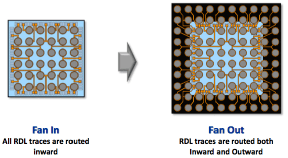
(Source:semiengineering)
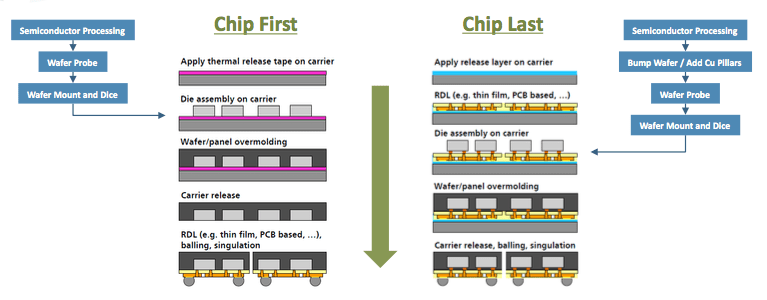
Chip first processing, in which the bare die was molded into a wafer shaped carrier with die pads exposed. Typically sputtering is used to provide interconnects to the die pad followed by patterned electroplating of redistribution lines (RDL) to “Fan Out” the next level interconnect pads to regions that can extend on to the molded material beyond the die perimeter. These processes require the use of relatively expensive semiconductor front end classes of equipment and are tailored to handle the reconstituted molded plastic wafers.
Chip last meets the needs of a large percentage of the applications requiring a packaging technology such as FOWLP. This new package has been in production in ASE for over a year, and uses a “Chip Last” approach to the problem of increasing useable interconnect pad area. Die which have been bumped with Copper(Cu) Pillars are mass reflowed onto a low cost coreless substrate, followed by over molding which also serves as the die underfill. The Cu pillars allow direct connection to die pads at 50 μm pitch or below, negating the requirement for RDL formation on the die.
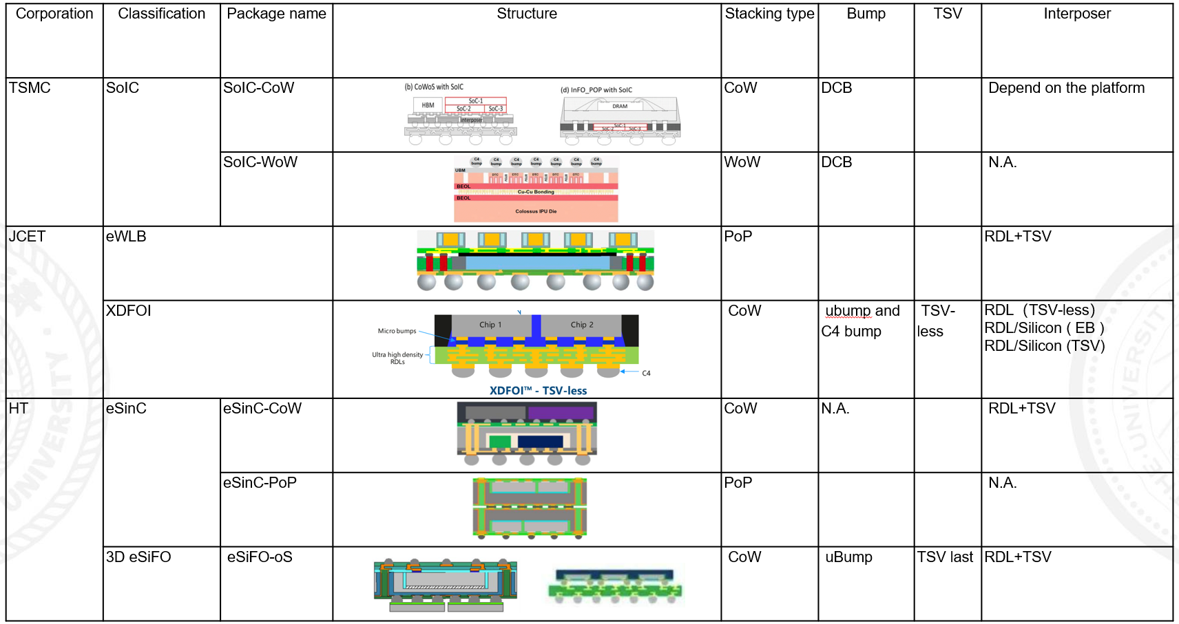
Main package technology
(Source:Unimicron Technology Corporation)
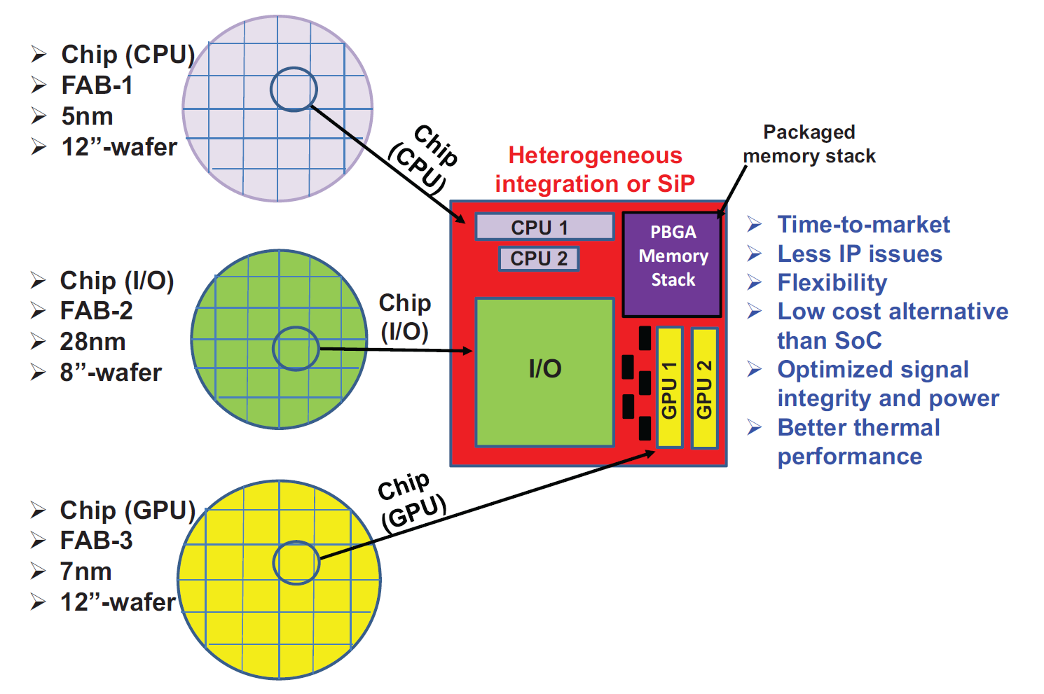
Heterogeneous integration (HI) is a general term used to represent the diverse possibilities for die technology incorporated into advanced 2.5D/3D packaging.
A complex HI package may incorporate:
-
3D (thinned die) high-bandwidth memory DRAM stacks
-
3D stacked die
-
a 2.5D interposer, with redistribution layers (RDL) for signal interconnects between die and the package substrate
And a hierarchy of attach technologies:
-
C4 bumps (~110-150um pitch)
-
microbumps for die-to-interposer attach (~40-55um pitch)
-
hybrid bonded (bumpless) attach, for 3D stacked die, in either a face-to-face or face-to-back orientation
-
through silicon vias (TSVs) in the interposer between the bumps and RDL layers
-
micro-TSVs through the silicon in the 3D die stack (~10um pitch)
There is also the potential to replace the silicon interposer with smaller silicon “bridges” between die edges in the 2.5D configuration, maintaining the high interconnect density while reducing cost (not shown in the figure above). The tradeoff with the use of bridges embedded in an organic substrate versus an interposer is the redistribution interconnect density is reduced considerably.
A key requirement of any heterogeneous integration system is the available bus bandwidth for data communication between die.
An electrical design consideration is whether the interconnect characteristics between die (on the interposer or bridge) will support wide parallel bus signaling at lower clock rates to achieve the requisite throughput, or whether a more sophisticated (and more power-hungry) high-speed serial interface design is required.
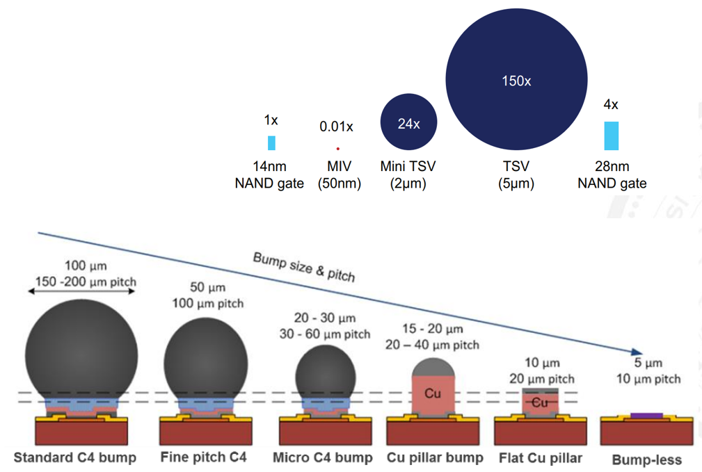
Relative size comparison of 3D vias and NAND gates (14nm and 28nm). The diameter of monolithic inter-tier via (MIV) is 50nm, mini TSV is 2μm, and TSV is 5μm (Source: GLOBALFOUNDRIES)
Significantly reduce the size of the encapsulated chip
Whether it is the encapsulation of multiple chips or the wafer-level encapsulation of a single chip, it can significantly reduce the size of the package to decrease the footprint of the entire system board. Utilizing packaging methods to shrink the chip area is more cost-effective than improving the front-end process.
Accommodate more I/O ports for chips
With the introduction of front-end process methods, we can use RDL technology to accommodate more I/O pins on a unit area of the chip, thus reducing waste of chip area.
Lower chip manufacturing costs
With the introduction of the chiplet approach, it becomes relatively easy to encapsulate multiple chips with different functions, process technologies/nodes together to form a system integration chip (SIP). This avoids the need for all functions and IPs to adopt the same (highest) cost method.
Enhance interconnectivity between chips
With the increasing demand for high computing power, in many application scenarios, there is a need for a significant amount of data exchange between computing units (CPU, GPU, etc.) and DRAM. This often results in almost half of the system's performance and power consumption being wasted on information exchange. Now, through various 2.5D/3D packaging methods, we can connect processors and DRAM as closely as possible, reducing this loss to less than 20%, thus significantly reducing the cost of computation. This efficiency improvement far exceeds the progress brought by adopting more advanced manufacturing processes.