BuildHardware
The design goals for the hardware:
- Simple to build by hand.
- No surface mount components.
- Cheap and easy to find components.
- Simple enough for breadboard build.
To fullfill those goals and the project goals, the following decisions was made:
- Use of Raspberry Pico which is cheap and have very good software support as well as the excellent PIO's making bitbanging the ACSI interface much easier.
- Use of a SD-MOD instead of surface mounted SD-Card slot.
- Use of IDC connectors and flat cable for RS-232, removing the need to keep track of connector pins and individual cables.
- RS-232 connector is DB-9 to require smaller flat cable, so a DB-9 to DB-25 adapter is needed for ST/STE.
- ACSI connector is built using pins through the PCB. This is a workaround for the inexistent ACSI DB-19 connector.
Example of a device with a DB-9 to DB-25 adapter. Ready to use on a ST/STE:
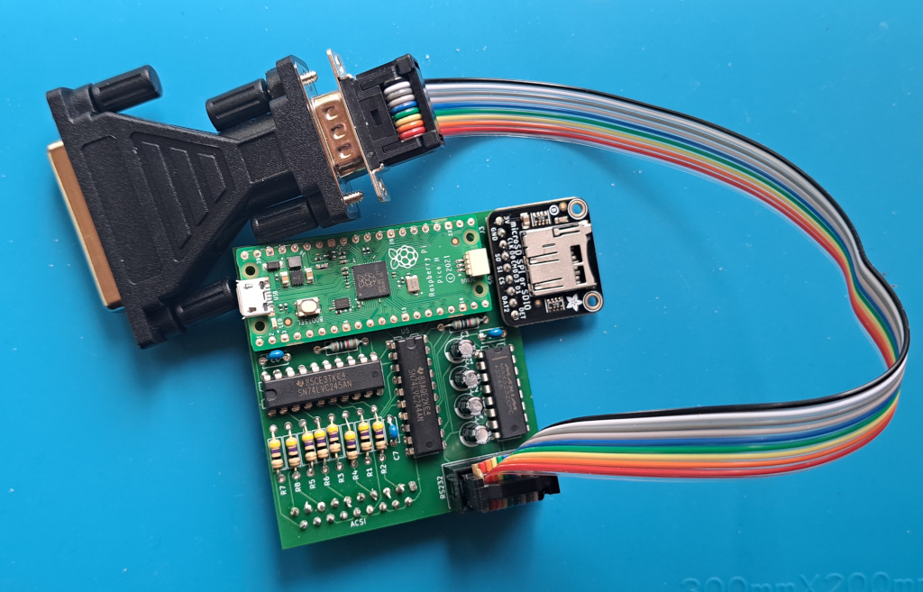
If you do not have KiCad installed to view the design files, then there is a pdf of the schematics if you need to have a closer look at something.
The PCB can be ordered from PCBWay.
NOTE!:
It is possible to order with components mounted, but do this on your own risk as no verification of proper mounting have been done!
RS-232 cable and ACSI pins are not part of the PCB components!
END NOTE
Parts list:
- 4x electrolyte capacitors 0.1uF 50v
- 3x ceramic capacitors 1uf
- 8x resistors 47ohm (33ohm to 100ohm acceptable)
- 2x resistors 10K ohm (2K ohm to 10K ohm acceptable)
- 1x MAX3232
- 1x 74LVC245 (must be LVC)
- 1x 74LVC244 (must be LVC)
- 1x Adafruit SD-Mod
- 1x Raspberry Pico H (with headers)
- 1x IDC header 2x5 male. Example.
- 1x IDC flat cable connector 2x5 female. Example.
- 1x DB-9 flat cable connector female. Example.
- 1x 10 conductor flat cable. Example.
- 1mm diameter wire or nails to use as ACSI pins.
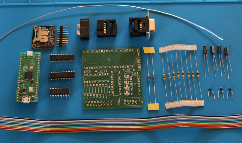
The steps building the device have been chosen from the assumption that the people needing this step by step guide are not experts and do not have expert equipment.
There are eight 47ohm resistors that protect the data lines and should be soldered to the R1, R2, R3, R4, R5, R6, R7 and R8 positions.
There are also two 10K ohm resistors that are used as pullup resistors that should be soldered to R9 and R10 positions.
The PCB should look like this:

The three IC's should be mounted as follows:
MAX3232 to position U1.
74LVC245 to position U2.
74LVC244 to position U5.
Be careful to place all IC's in the correct direction! Line up the notch in the IC with the symbol on the PCB like this:
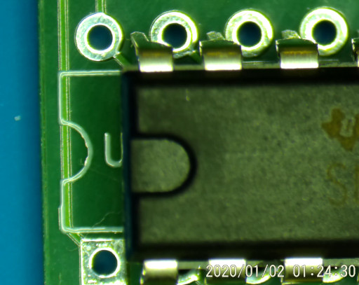
When the IC's are soldered, the PCS should look like this:
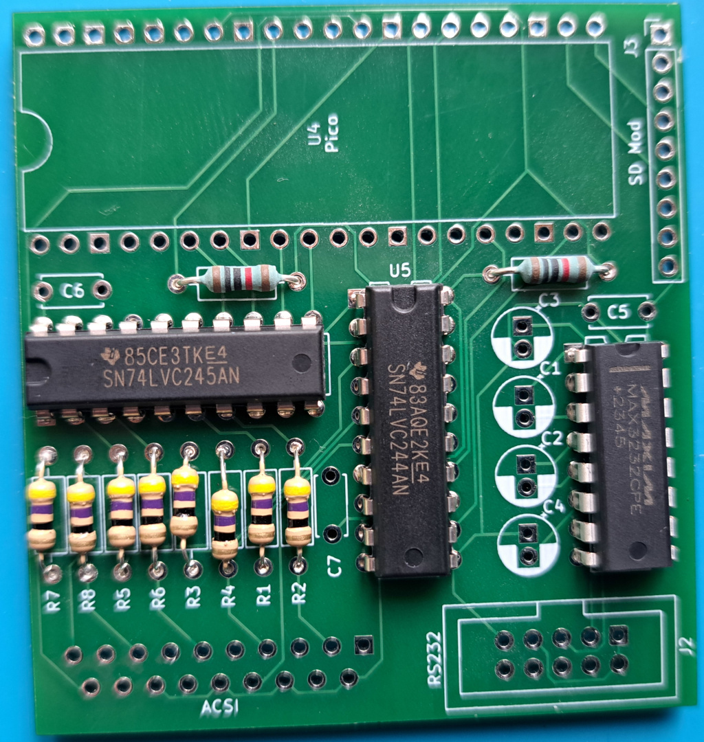
There are three ceramic 1uf capacitors that are used as decoupling capacitors for the IC's. Solder them to the C5,C6 and C7 positions and make the PCB look like this:

There are four electrolyte capacitors used to charge pump current to RS-232 levels. They should be soldered to C1,C2,C3 and C4 positions, and the pins are positive and negative and must be placed in the correct holes.
This image shows how electrolyte capacitors have a light colored band on one side. This band should match up with the filled side of the circle on the PCB.

When soldered it should look like this:

And when all electrolytes are in place, the PCB should look like this:
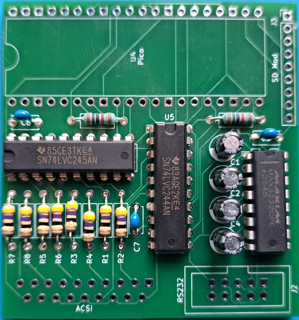
It is assumed that you have a Raspberry Pico H, where the headers already are mounted.
Place the Pico on the U4 position and make sure the USB port is to the left on the PCB.
After soldering the Pico, you should have a PCB looking like this:
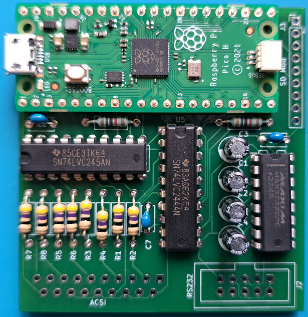
The SD-Card Mod from Adafruit comes with a pinheader. This pinheader may be too long and in that case, just cut it to correct length.
First solder the pinheader to the SD Mod position. Be careful with heating the pinheader as the plastic melts quite fast.
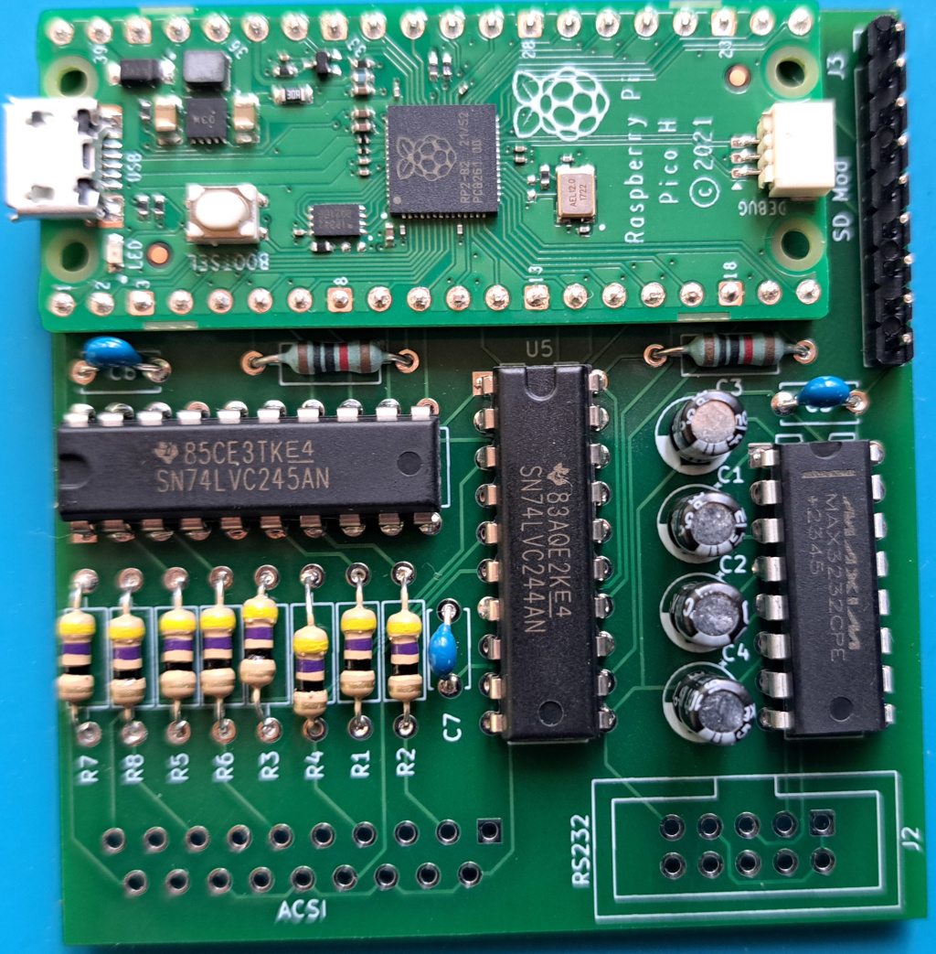
Next solder the SD-Card Mod to the pin header and make the PCB look like this:
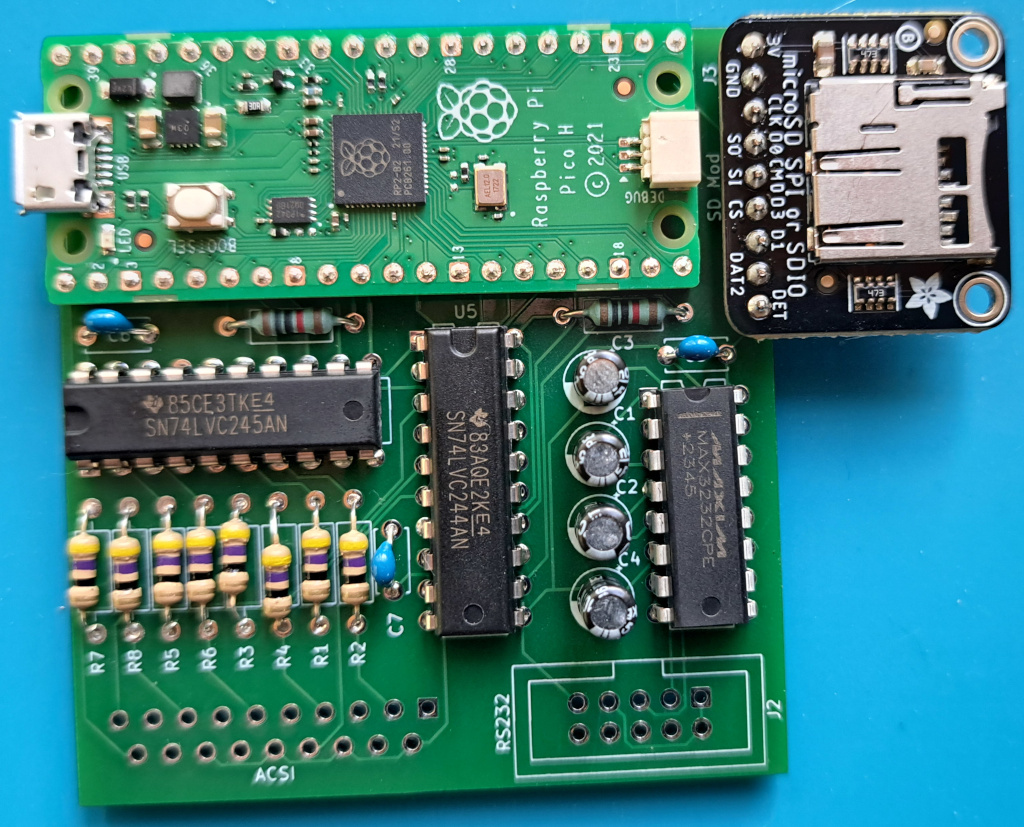
This step is needed if you will build the flat cable later.
If you plan on soldering your own cable directly to the PCB, then this step can be skipped.
Solder the male IDC header to the J2 position and make sure to place the notch upwards.
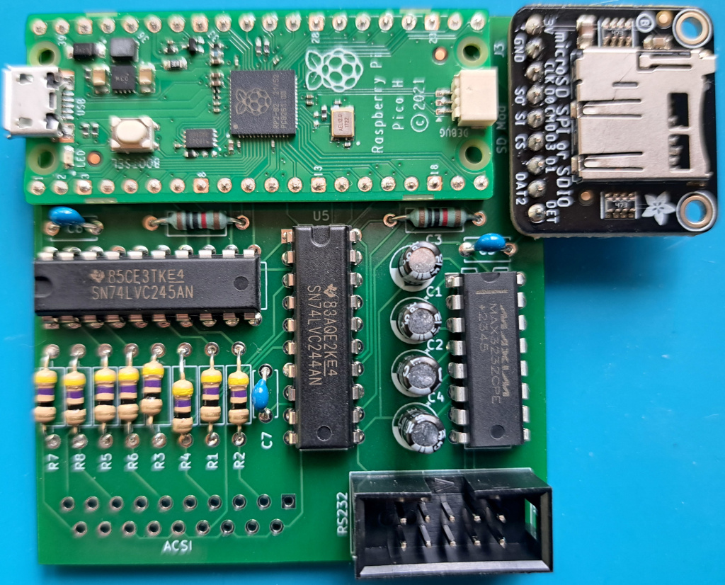
This is the hardest part for a beginner to solder.
The steps below have been chosen specifically to increase the chances of success.
In this example, the pins are made of a 1mm steel wire that I found in the local hardware store.
The first trick is to have a female DB-25 connector to use as a pinholder. In my case I use a DB-9 to DB-25 adapter:


Then I put the wire through a hole in the PCB and into the DB-25 connector as far as it goes:

I cut the wire and put it through another hole:

And cut the second wire and solder both.
As the wire is thick and long, it needs more heat to solder than ordinary components and some soldering pens may struggle to deliver enough heat.
When this is done we will have a more stable platform:

Now we just need to repeat the work and put a wire into every ACSI hole:
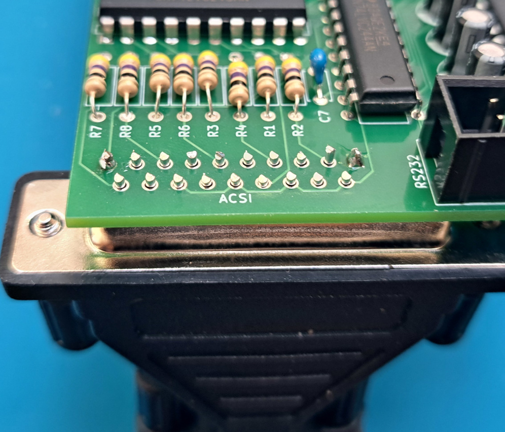
Solder all the pins and remove the DB-25 connector. If you turn the PCB around, it should now look like this:
(NOTE: there should be no empty unsoldered holes in the PCB)
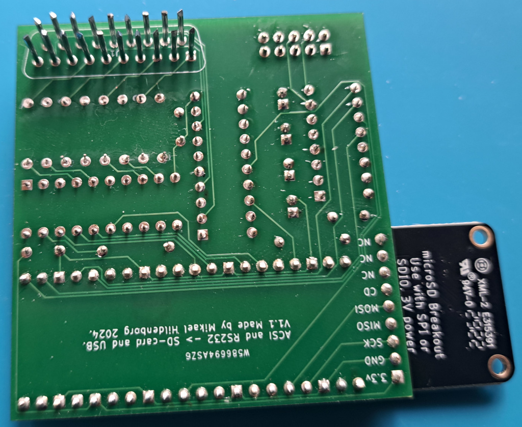
The cable is designed to be quick to build without having to keep track of which cable should go to which pin.
There are many different flat cable IDC connectors, so the one you use may differ in how it is assembled.
The vital part in any case, is to keep track of how the flat cable is oriented to the connector. In the image below, I have decided to place the IDC connector with the
notch up and the color coded flat cable with the black conductor to the right side of the IDC connector:

First put the flat cable through the connector and press hard on the connector to close it up:
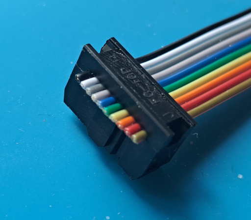
In case your connector have pull out protection, then wrap the cable around:
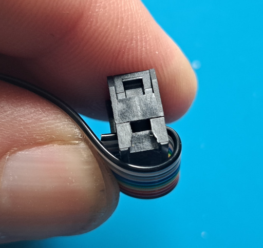
And put the pull out protection in place:
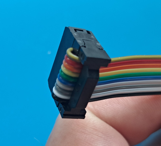
The finished contact looks like this:
(NOTE: the black conductor is to the right.)

The IDC connector needs ten conductors, but the DB-9 connector can only take nine. So we need to remove one conductor.
Use your nails (or a sharp knife) to separate the outmost conductor on the opposite side of the black conductor:
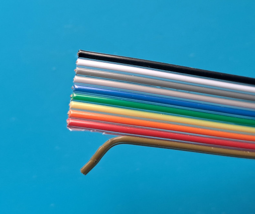
Then pull it lose all the way to the IDC connector and cut it off.
It should look like this:
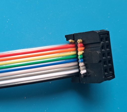
As with the IDC connectors, there are many variants of how the DB-9 connector is assembled. And like the IDC connector, the vital part is how the flat cable is oriented to the DB-9 connector.
In this case we orient the DB-9 connector and cable so they go together like this:
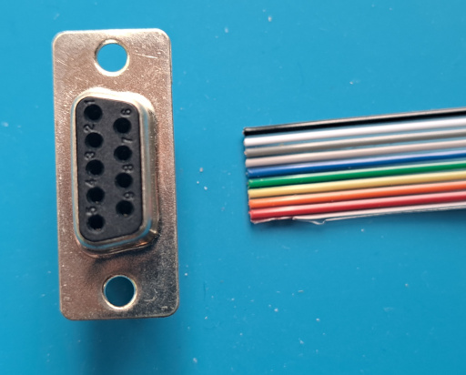
Insert cable and press connector together to get this:
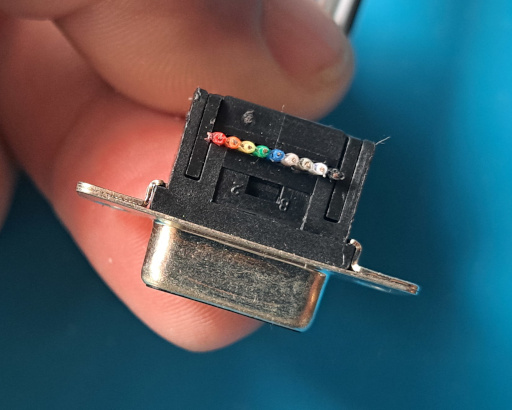
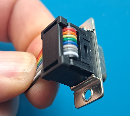
And with the pull out protection:
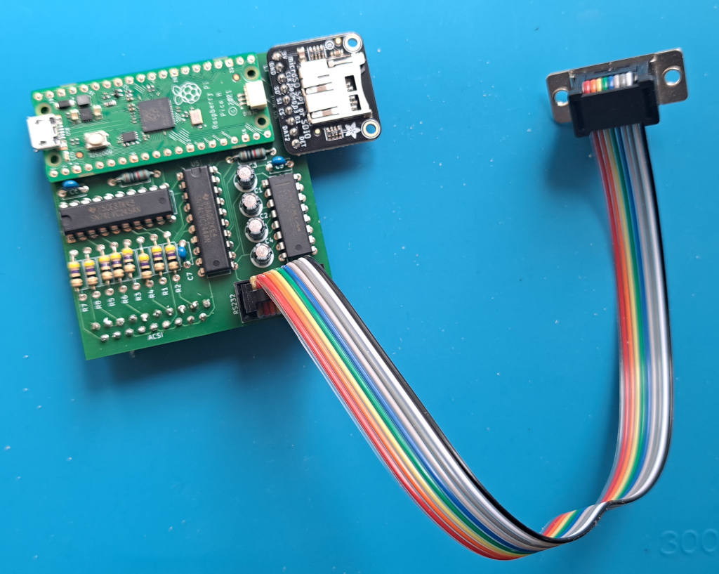
When all is done and the cable is plugged into the device, this is what you should see:
The device must be flashed with firmware and have a SD-Card with hard disk images in it to work.
Go to: Atari-Link releases and download the latest "atari-link.zip" release and unpack it.
On the Pico mounted on the device, press and hold the "bootsel" button while connecting a USB cable between the Pico and your PC.
A USB drive should appear on your PC and you can release the "bootsel" button.
From "atari-link.zip", drag and drop the file "atari_link.uf2" to the USB drive.
Disconnect the Pico USB cable.
Format a SD-Card in a FAT compatible format.
From "atari-link.zip", copy the following files to the SD-Card:
"tos32mb_ahdi5_boot.img"
"tos32mb_gdbsrv.img"
"config.txt"
Insert the card into the device.
It is assumed that you do not have any hard disk connected to your Atari.
If you do, then you need to change the "AcsiId" in the "config.txt" file.
Put the device into your Ataris ACSI port and insert the RS-232 connector into the modem port.
Connect a USB cable between the device and your PC.
This should make a USB drive appear. This drive contains two files: "GDBSRV.GTP" and "GDBSRV.TTP". This is the "tos32mb_gdbsrv.img" that is visible as a USB drive.
Now start your Atari and it should boot the image: "tos32mb_ahdi5_boot.img"
If you have another SD-Card Mod or want to connect to an SD-Card another way, then the image below shows you how the Raspberry Pico pins are connected to the SD-Mod header pins.

If you want to build your own RS-232 cable or solder a cable directly to the PCB, then this is how you do it.
First you need to know that the RS-232 port on the PCB is null-modem prepared, meaning that a straight cable (as in the example above using flat cable) will automatically produce a null-modem cable which is what is needed.
The RS-232 pins on the PCB is numbered as the image below shows:
 The pin number 10 is unused and unconnected.
Pin 1 to 9 can be straight connected to pin 1 to 9 on a DB-9 connector to get a working cable.
To connect the PCB pins to a DB-25 connector, then connect the pins using this table:
| PCB pin | DB-25 pin |
|---|---|
| 1 | 8 |
| 2 | 3 |
| 3 | 2 |
| 4 | 20 |
| 5 | 7 |
| 6 | 6 |
| 7 | 4 |
| 8 | 5 |
| 9 | 22 |
The device will provide a hard disk emulator that also connects as a USB stick.
It also provides a USB to RS-232 null modem cable.
The setup using the released firmware and hard disk images will provide the Atari with: one boot disk where the Atari can read and write to, and one development disk where gdbserver resides. The development disk is read only to the Atari while USB can read and write to it.
This is a setup that is specifically made for general Atari development and have been tested on computers from Atari 520ST with TOS1.4 up to TT and EmuTos.
It is now possible to modify the example projects from m68k-atari-dev toolchain, to use the device USB drive and serial connection to remotely execute and debug software for Atari using an IDE such as VsCode.