

This is a repository on RTL Design using Verilog with Sky130 Technology workshop conducted by VSD.It is a day by day log including examples from Lab sessions and Theory sessions
- Introduction
- Day 1 Introduction to Verilog RTL Design and Synthesis
- Day 2 Timing libs Hierarical vs Flat Synthesis and efficient Flop Coding Styles
- Day 3 Combinational and sequential optimization
- Day 4 GLS blocking vs non blocking and Synthesis Simulation mismatch
- Day 5 Optimization in synthesis
- Observations
- Acknowledgement
- References
This Workshop intends to teach basics of digital design using verilog language, various RTL coding styles,synthesis and problems faced by industry and how to solve them in Verilog using SKY130 Technology.
Some of the open source eda tools used in this Workshop are
- iverilog : It is Simulator which used for RTL Simulations and Gate Level Simulations.
- yosys : It is a open source Synthesis tool used for synthesis of RTL Design.
- Skywater: It is used as 130nm Standard Cell Libraries.
Simulator
RTL design is checked adherence to the spec by simulating the design.Simulator is the tool used for simulating this design.
We have used iverilog in this workshop for simulation.
Design
Design is the actual Verilog Code or set of verilog codes which has the intended functionality to meet with the required specifications.
TestBench
TestBench is setup toapply stimulus (test vectors) to the design to check its Functionality.
How the Simulator Works ?
- Simulator looks for changes in input signal.
- Upon change in input the output is observed.
- If there is no change to the input there will be no change to the output.
- Simultor looks for changes in the Value of input.
The TestBench looks something like this

Note:
Design may have 1 or more primary inputs,1 or more primary outputs. TestBench doesn't have a Primary inputs or a primary outputs.
iverilog Based Simulation
- Design and Testbench are given to iverilog.(As we know any simulator looks for the changes in input.)
- The output of iverilog simulator is vcd file.
- Here vcd stands for Value Change Dump format.
- To view the vcd file we use another tool called GTKWave which is used for viewing the waveforms.
LAB Session
Lab 1
It is introductory lab session in which we look at environment setup for running the labs.
Before cloning we can create directory vsd and inside it another directory VLSI using the mkdir command as demonstrated below
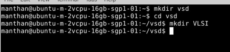
After creating the VLSI directory. We have to clone a repository named sky130RTLDesignAndSynthesisWorkshop which contains the required library files and verilog design files to perform the simulations and logic synthesis parts of the workshop. It can be done using by using basic linux command git clone git clone https://github.com/kunalg123/sky130RTLDesignAndSynthesisWorkshop.git as demonstrated

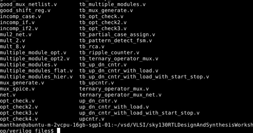
After succesfully cloning it creates a sky130RTLDesignAndSynthesisWorkshop directory inside the VLSI directory. It contains various files required for this workshop you can explore the files such as my_lib which contains the library files lib and verilog_model.verilog_files which contains various verilog codes and its testbench files for all the lab expirements.


Lab2
In this Lab we are introduced to iverilog and GTKwave.
Step 1 : We use the command iverilog to load the simulator follwed by the verilog file and testbench name. a.out file is created in the verilog_files folder

Step 2 : After creating a.out file we execute it using ./a.out it is going to dump the vcd file

Step 3 : Then we write the command gtkwave followed by the vcd file name like gtkwave tb_good_mux.vcd

We get the following waveform of a 2:1 Multiplexer when sel = 0 output follows i0 and when sel = 1 output follows i1 in the GTKWaveform viewer
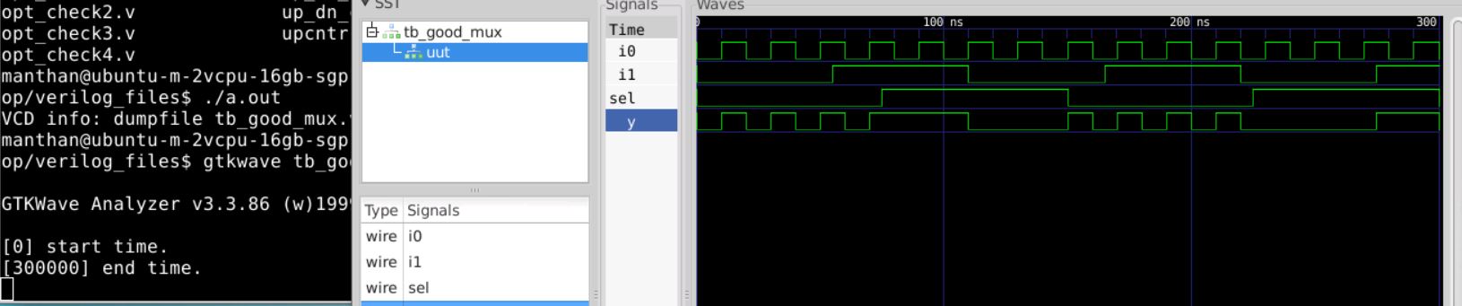
We also observe the verilog code of the good_mux.v and tb_good_mux.v by using the command gedit (also vim and gvim can be used in systems where gvim it is installed)

We get the good_mux.v verilog code .There are various codes to generate a MUX we have used the if statement for it

and the testbench tb_good_mux.v we can see the instantiation of design and the stimulus generator and it runs for 300ns.

Introduction to yosys
Sythesizer
It is a tool used for converting RTL to Netlist . We use Yosys synthsizer used in this course.
How does Yosys work ?
We have a design and .lib file and it is given to the yosys tool which gives out the netlist.
Commands for using Yosys
read_verilog--> To read the design.read_liberty--> To read the .lib.write_verilog--> To write out the netlist file.
Note
Netlist file is the representation of design in the form of Standard Cells present in the .lib .
Verification of Synthesis
The GTKwave should be as we found in the case of design simulation as Netlist is just the cell representation of design they both are basically the same.
Note
The set of Primary inputs/primary outputs will remain same between RTL design and Synthesized Netlist --> Same Testbench can be used.
Logic Synthesis
RTL design
It is the Behavioral Representation of required specification like the verilog HDL code below
module sample_code(
input clk,rst,
output result,done);

always @ (posedge clk,posedge rst)
if(rst)
---
else
---
endmodule
--------------
--------------
Synthesis
- RTL to Gate Level Translation
- The design is converted into the gates and connections are made between the gates.
- This is given out as the file called Netlist.
.lib file
- It is the collection of the logical modules
- Includes basic gates such as And,Or,Not etc.
- Different flavour of same gate
- 2 input And Gat
- slow
- medium
- fast
- 3 input And Gate
- slow
- medium
- fast
- 4 input And Gate ....
- 2 input And Gat
Why Do we need different flavours of gates
As the combinational delay in the logic path determinesthe maximum speed of operation of digital logic circuit i.e
Tclk > TCQ_A + Tcombi+TSetup_B we need cells to work fast
And to ensure that there is no hold issue in the next flop we need slow cell and as hold time is given by
THold_B < TCQ_A + Tcombi we need cell that work slowly.
We need cells that work fast to meet performance and cells that work slow to meet Hold time. So we need different flavours of gate to meet this requirement.The Collection forms .lib.
Note
Load in Digital Logic Circuit --> Capacitance
Faster the charging/discharging --> Lesser the cell delay
- To Charge/Discharge the capacitance fast, we need Transistors capable of sourcing more current.
- Wider Transistor --> Low Delay --> More Area and Power.
Selection of Cells
- Need to guide the synthesizer to select he cells that are optimum for implementation of logic design.
- More use of Faster cells results in bad circuit in terms of area and power and also might voilet the Hold time.
- More use of slower cells results in sluggish circuit.
- The Guidance given to the synthesizer is known as 'contraints'.
Lab 3
Synthsis using Yosys
Step 1 : First we Invoke the Yosys by simply typing the command yosys.
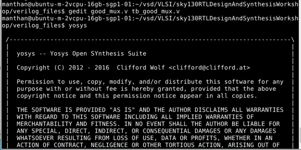
Step 2 : We are in the yosys prompt now, then we read the library using read_liberty -lib followed by path of the library it will import the library

Step 3 : Then read the design using the command read_verilog.

Step 4 : After the design is read successfully we use use the command synth -top for telling what module to synthsize
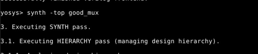
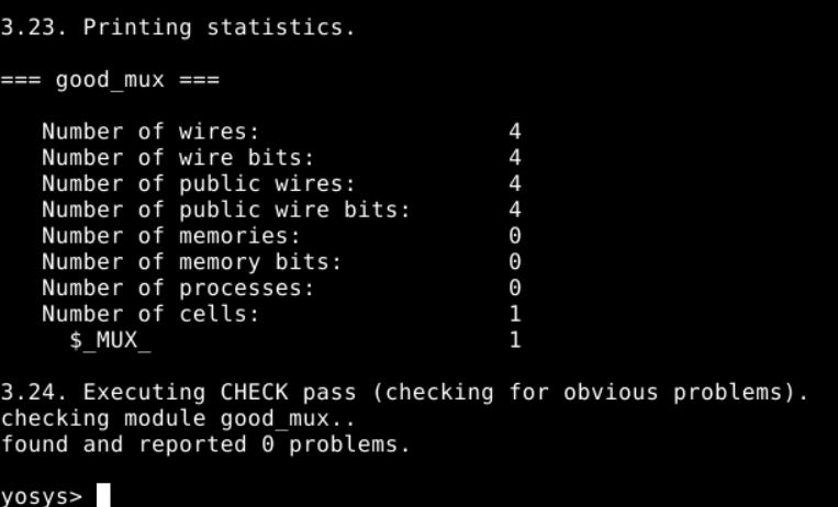
Step 5 : Now to generate the netlist we use the command abc -liberty followed by the location of .lib file.

We can see what all internal signals ,input and output cells it has inferred
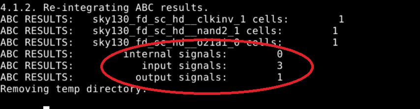
Step 6 : Now to see the Logic it has realised type the command show
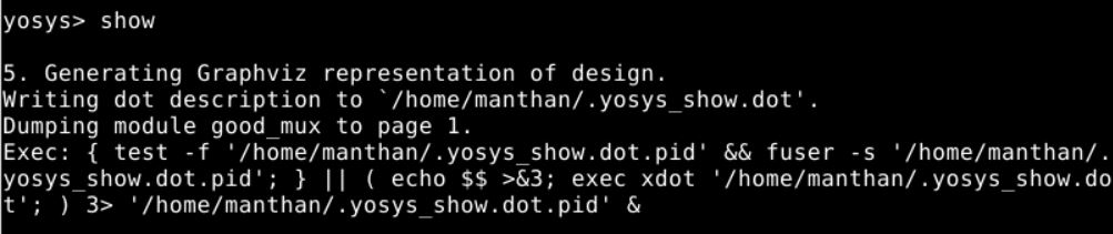
We get the following Logic Implementation.
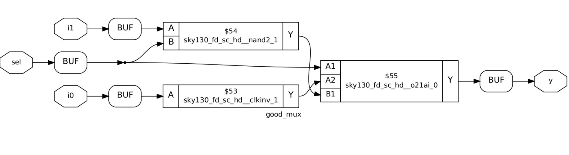
In the Logic Circuit generated we observe
- nand2_1 --> 2 input Nand gate
- o21ai_0 --> or and inverter
- clkinv_1 --> inverter
We get the Output from the logic circuit as y = i1 sel +i0 sel' which is the logic for 2 input Multiplexer.
We have used sky130_fd_sc_hd__tt_025C_1v80 for which meaning of each abbreviation is given below
- fd - the skywater foundary
- sc - digital standard cell
- hd - high density
- tt - typical process
- 025C - temperature
- 1v - voltage
Note
library in the sky130 pdk are named using the following scheme:
process name _ library source _ library type _ library name
Here is sample of .lib file
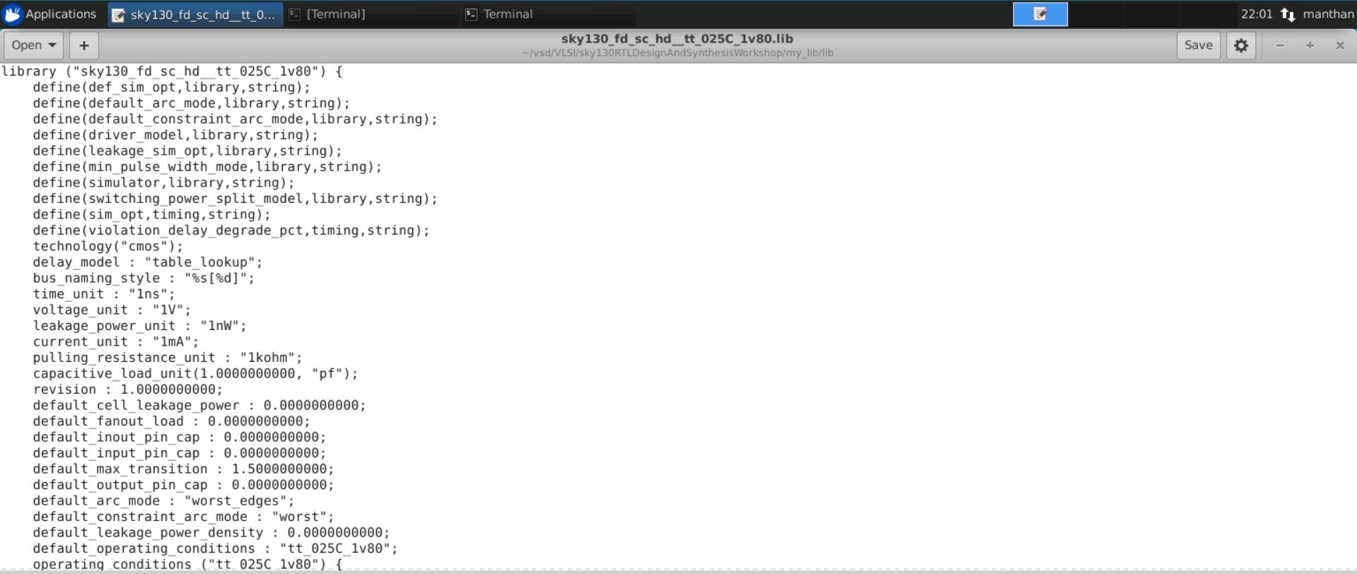
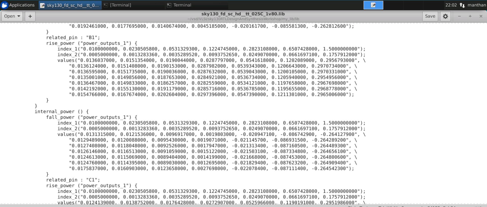
Some details which are provided in the .lib file are
- Power
- Internal Power
- Leakage Power
- Area
- Pin details
- Timings
- Capacitance
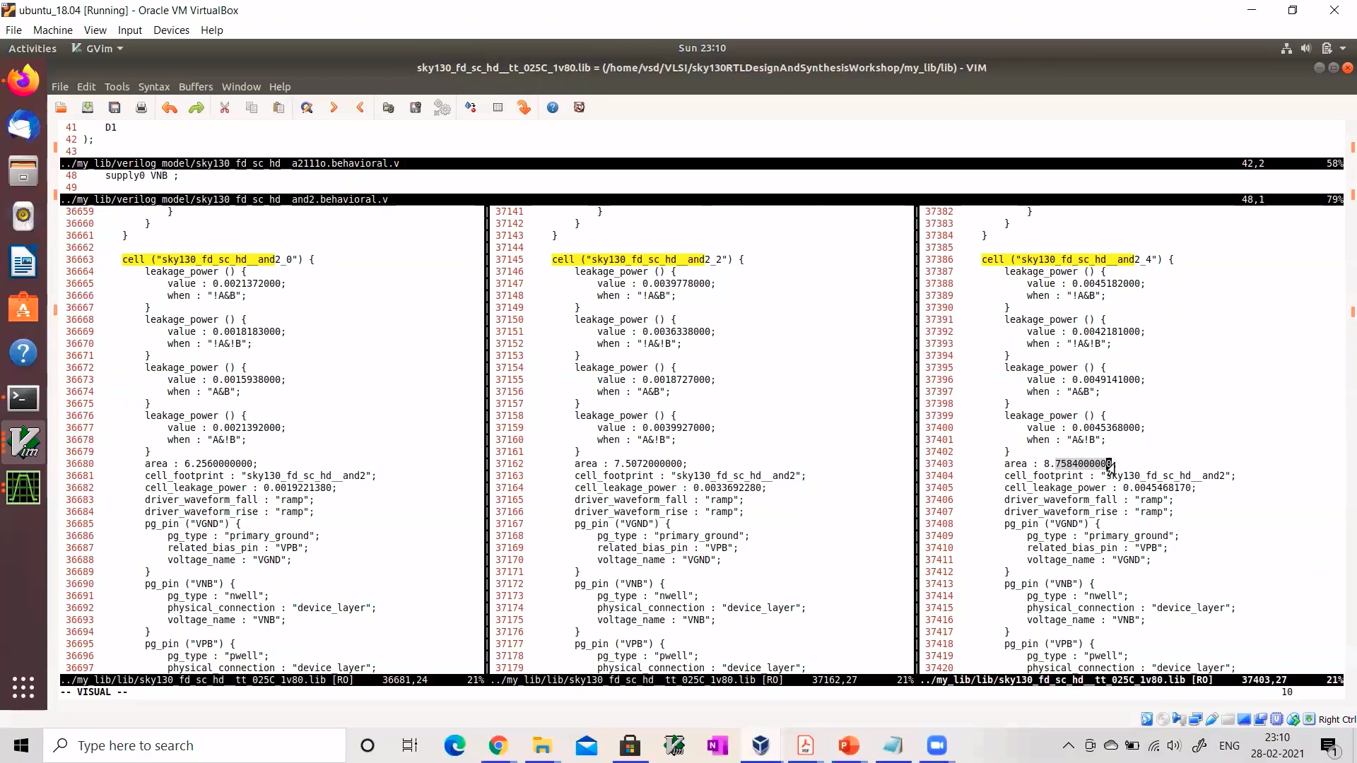
Note
Here we observe that
area(and2_4) >area(and2_2)>area(and2_0)
power(and2_4)>power(and2_2)>power(and2_0)
In this section we explore through the Hierarical and Flat synthesis.
Let us go through one of the examples through a Lab session to understand the difference between hierarchical and Flat Synthesis.
LAB Session
Lab 1
For this we are going to consider the multiple_modules.v code.\
module sub_module2 (input a, input b, output y);
	assign y = a | b;
endmodule

module sub_module1 (input a, input b, output y);
	assign y = a&b;
endmodule


module multiple_modules (input a, input b, input c , output y);
	wire net1;
	sub_module1 u1(.a(a),.b(b),.y(net1));  //net1 = a&b
	sub_module2 u2(.a(net1),.b(c),.y(y));  //y = net1|c ,ie y = a&b + c;
endmodule
Step 1 : Invoke yosys using yosys
Step 2 : Read liberty file using read_liberty

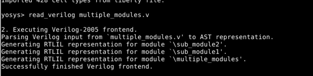
Step 3 : Read verilog file using read_verilog
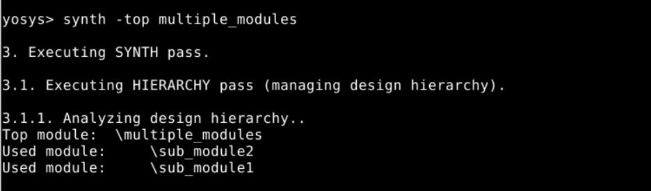
Step 4 : For starting the synthsis process use synth -top and also observe the inferences
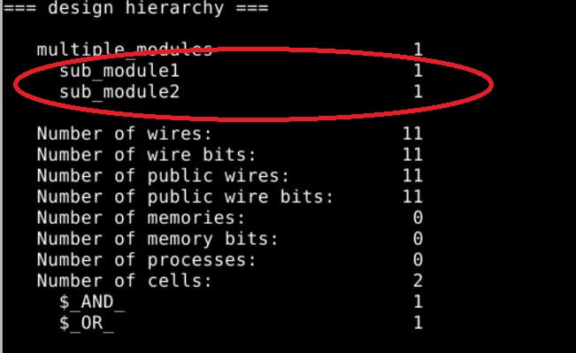
Step 5 : Now to map to standard cell we use abc -liberty
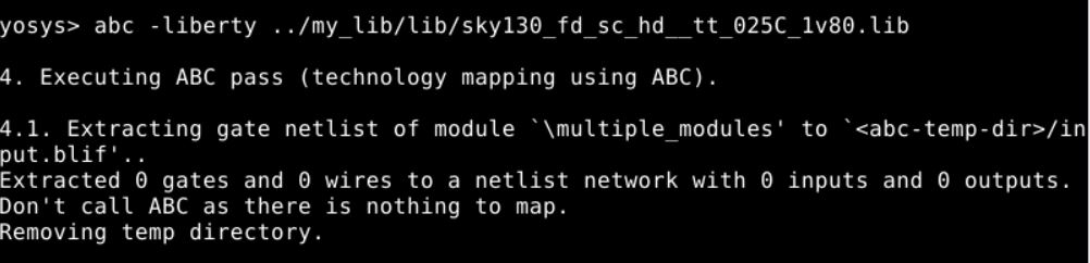
Step 6 : Now to see the Logic design we give the command show
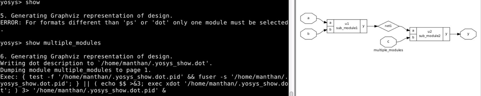
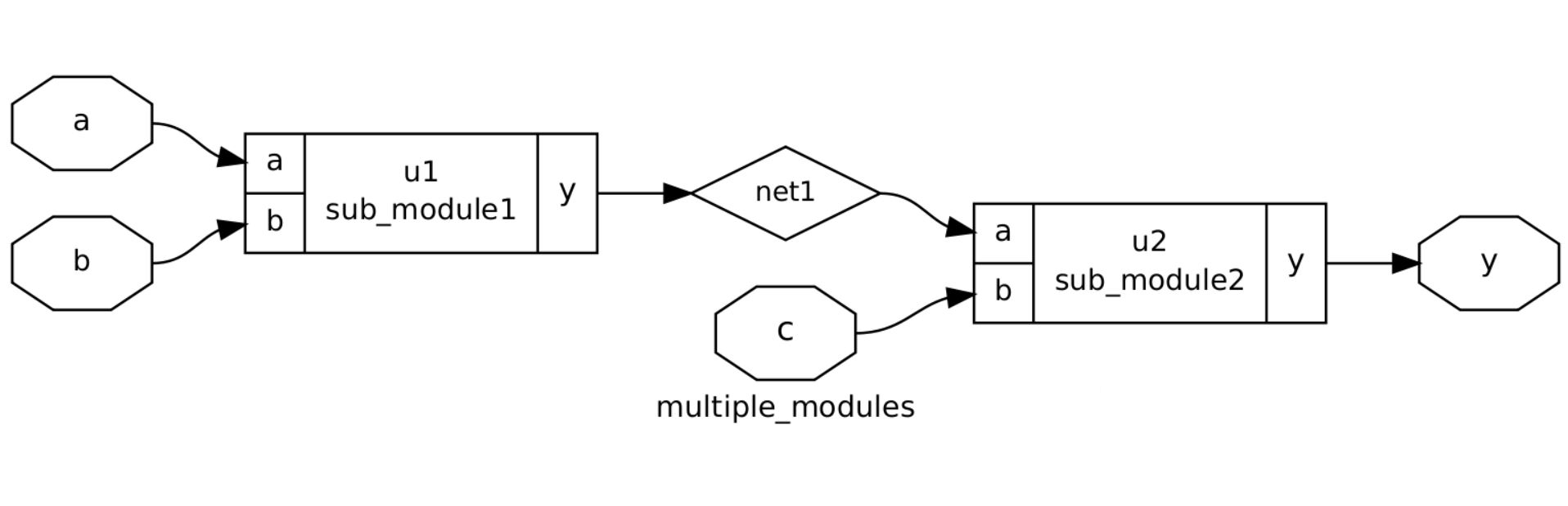
We observe that it does not show 'and' gate or 'or' gate but instead shows the 2 sub modules u1 and u2.This is what we call the Hierarical design.
Step 7 : Now to get the netlist we give the write_verilog -attr command
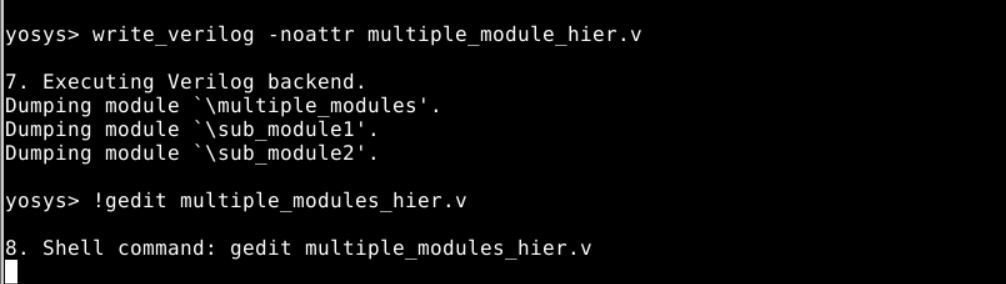
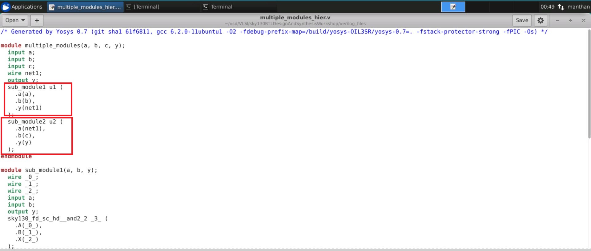
We see that all the hierarchies are preserved and to avoid stacked PMOS the logic is implemented using NAND gates.
Note
Stacked PMOS is always bad because PMOS has poor mobility and to improve this we have to make the cell alot wide cell to get good logical effort.
Step 8 : We use flatten to write out he flat netlist.And again use write_verilog -attr to get the flattened netlist.
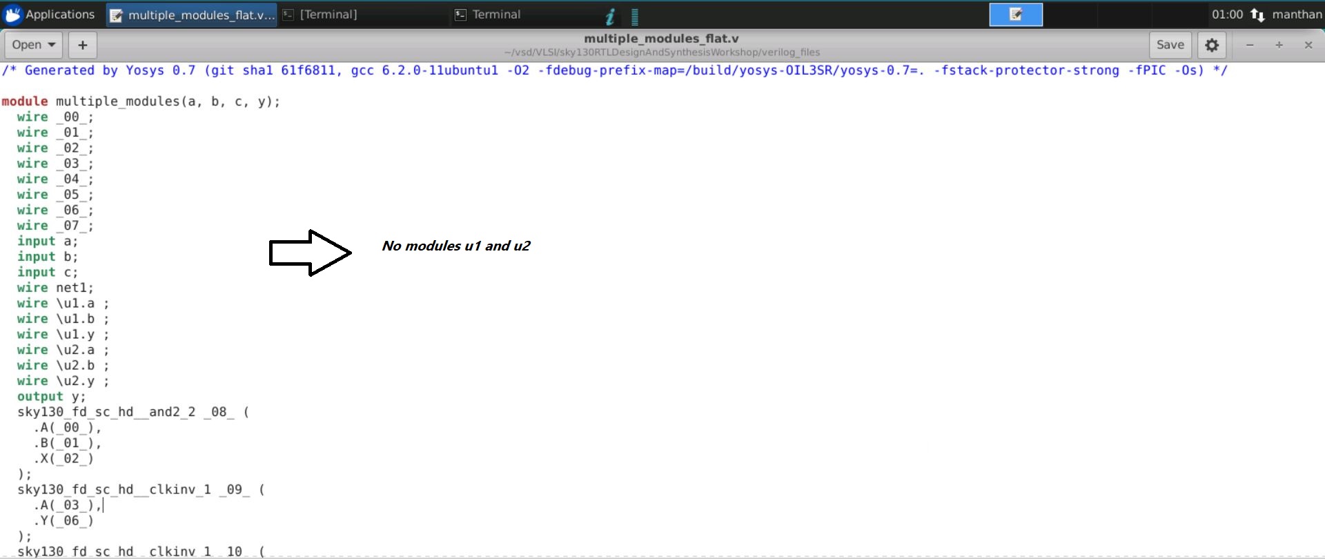
In this case the hierarchy is not preserved but are flattened out. We can see the logic diagram flattened as below
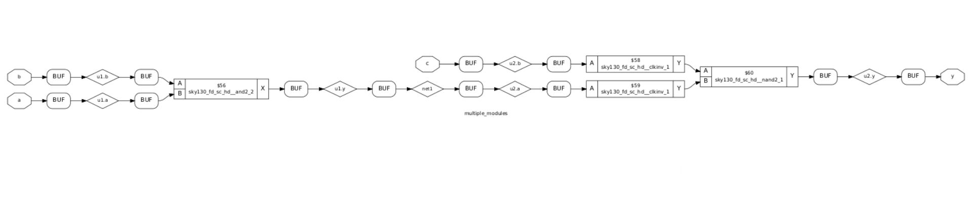
We do not see u1 and u2 but the sub-modules completely flattened.
Now to do a sub module level synthesis we follow the same procedure until Step 3
Step 4 : Instead of synth -top to get sub module level syntheies we give the command synth -top sub_module1
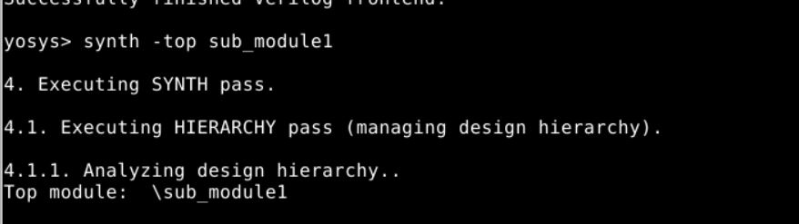
again follow the Step 5 and Step 6.We get the logic diagram of sub_module1.
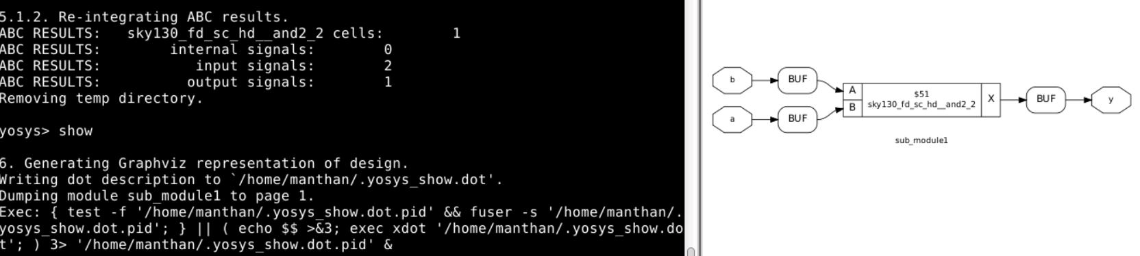
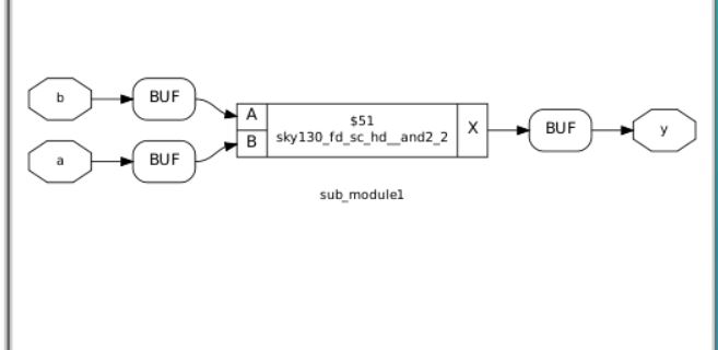
- When we want to use multiple instances of the same module.
- We want to do divide and conquer approch if we have a massive design.
Note
Synth -topcontrols which module to synthesis.
flattenis used for flattening the netlist.
Let us understand this concept using an example.
Take dff_asynres.v
module dff_asyncres ( input clk ,  input async_reset , input d , output reg q );
always @ (posedge clk , posedge async_reset)
begin
	if(async_reset)
		q <= 1'b0;
	else
		q <= d;
end
endmodule
Now let simulate it using the same steps above
After Simulation we get the following waveform

We observe from the waveform that when reset went zero the output q did not wait for the rising edge of the clock to change its value to 0 it immediately became 0.
Now let us take the dff_syncres.v
module dff_syncres ( input clk , input async_reset , input sync_reset , input d , output reg q );
always @ (posedge clk )
begin
	if (sync_reset)
		q <= 1'b0;
	else
		q <= d;
end
endmodule
Now let simulate it using the same steps above
After Simulation we get the following waveform
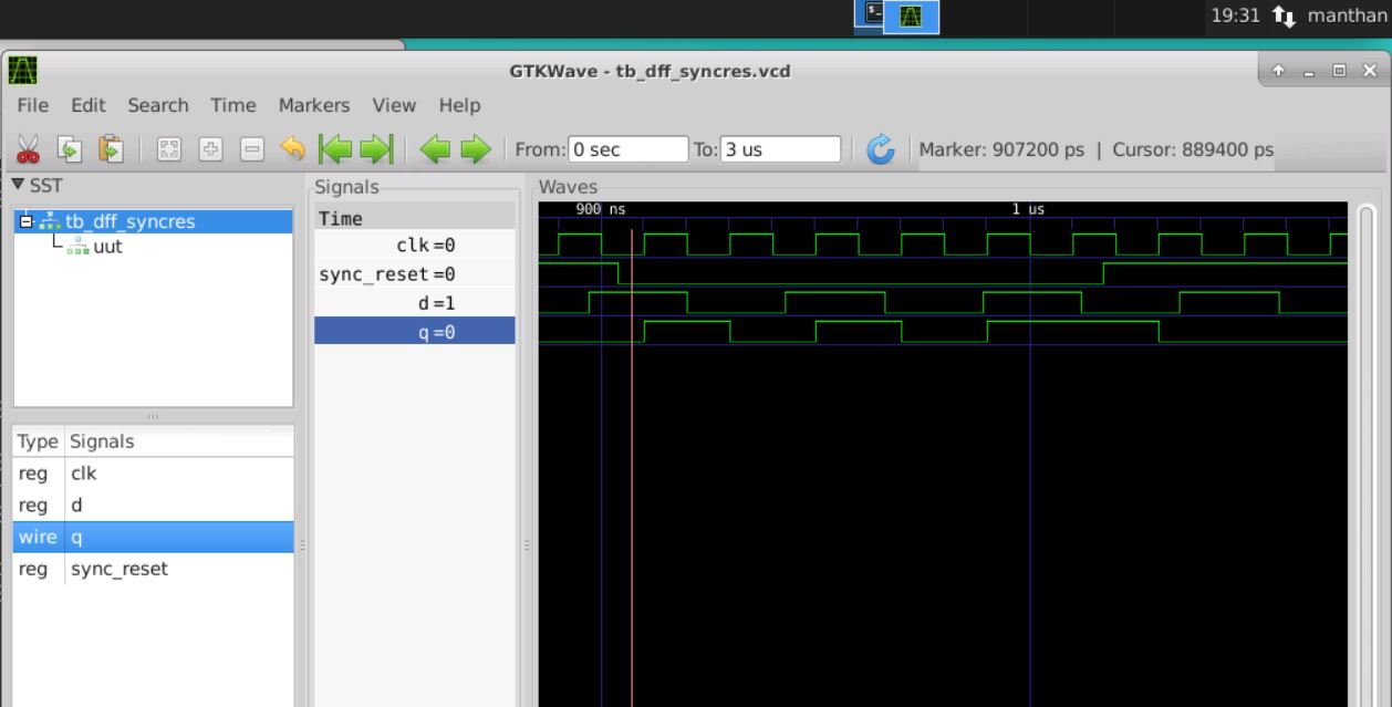
We observe that after output q waits for rising edge of clk to change the value after reset is high.
Logic Optimisation contains mainly 2 parts
- Combination Logic Optimisation
- Sequential Logic Optimisation
- We need combinational logic optimisation to squeeze the logic to get the most optimised design
- Mainly for Area and Power Saving
- Constant Propogation is one of the technique used for Combinational Logic Optimisation
- It is a Direct Optimisation in which the value of one input is propogated to the next stage to get the most optimised logic.
- Another Technique Used is the Boolean Logic Optimisation in which we use and other tools to get the most optimised logic.
In Sequential Logic Optimisation there are 2 Techniques
- Basic
- Sequential Constant Propogation
- Some of the Sequential design in which D input is tied off the Squential Constant is propogated to give Q pin as a Constant and gives the most optmised design of the Squential Circuits.
- The Sequential Design in which Q does not remains as constant cannot be optimised and flop needs to be retained in the circuit.
- Note
Every flop in which the D input is tied off is a sequential constant for the flop to become sequential constant the Q pin should always take a constant value.
- Advanced (not a part of the workshop)
- State Optimisation
- Optimisation of unused states.
- Retiming
- It is a Technique to improve the Performance of the Circuit.
- Sequential Logic Cloning (Floor Plan Aware Synthesis)
- It is done when we are doing a Physical Aware Synthesis.
LAB Session
Lab 1
Combinational Logic Optimisation
In this Lab we are going to use all the 'opt_check' files which can be found by typing the commandls *opt_check*
Let us first see the code for opt_check.v and opt_check2.v by opening it using gedit

The opt_check is simplified as y = ab (And Logic gate)
The opt_check2 is simplified as y = a+b (Or logic gate)
Step 1 : Now we invoke Yosys using the command yosys
Step 2 : Load the Libraries using read_liberty -lib
Step 3 : Now read the verilog file using read_verilog
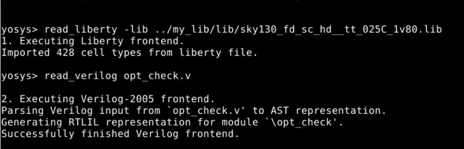
Step 4 : Now synthesizing the device using synth -top
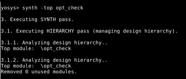
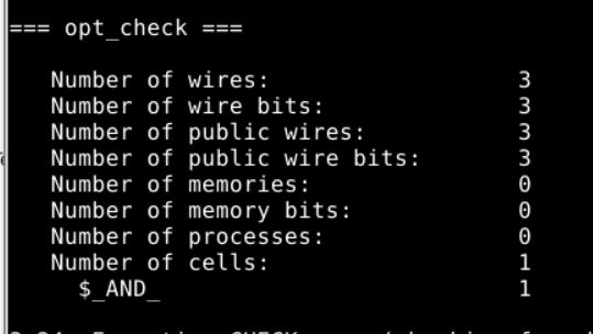
Step 5 : The Command to do the constant propogation and all the optimisation is opt_clean -purge

Step 6 : Now Link it to the liberty using abc -liberty and then show

As we already concluded earlier for opt_check.v we are getting an And gate we see the same being implemented.
Similarly we check the implementation for opt_check2.v.
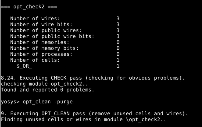
As we already concluded earlier for opt_check2.v it should be a 2 input Or gate we get the same being implemented.
As Or gate involves Nor gate and it uses a stacked PMOS which is bad due its mobility and various other reasons the so the Tool does a Nand Realisation of Or gate.It a inverter -inverter followed by a Nand.

Similarly we observe opt_check3.v.

We evaluate that y = abc (3 input And gate).We apply the same process as above for opt_check.v and opt_check2.v to get the optimised output.

As we already concluded earlier for opt_check3.v it should be a 3 input And gate we get the same being implemented.
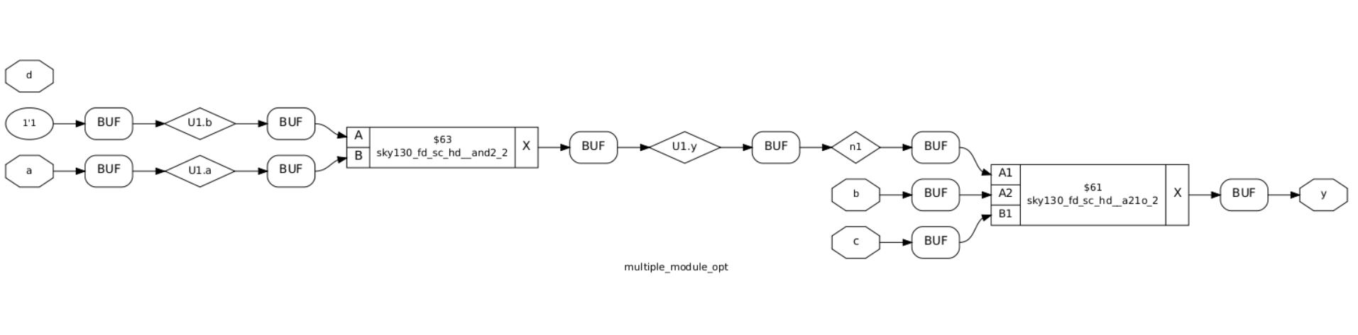
Similary We observe multiple_modules_opt.v.
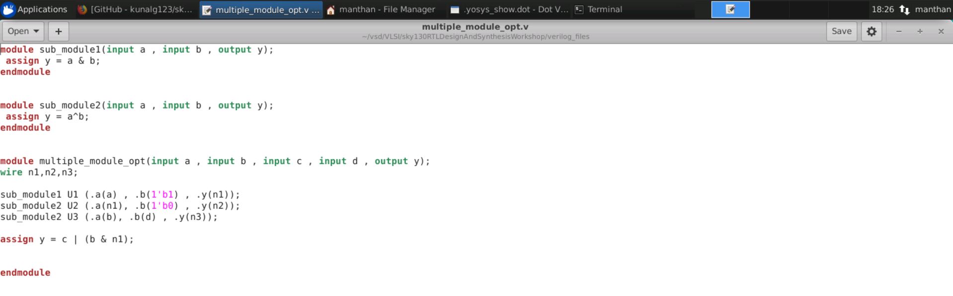
We get the following result after we flatten the multiple_module_opt
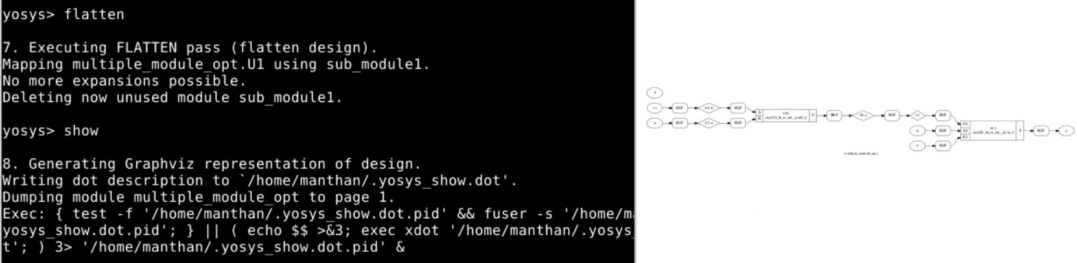
The resulting Circuit is Enlarged below
Sequential Logic Optimisation
Lab 2
In this Lab we are going to use all the 'dff_const' files which can be found by typing the commandls *dff_const*
Let us take the dff_const1.v and dff-const2.v and open it
Here is the Verilog code for both

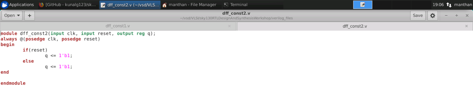
Step 1 : Let us simulate before synthesizing for that we use iverilog and then excute the a.out file to get vcd file.
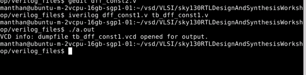
Step 2 : Use gtkwave to get the waveform
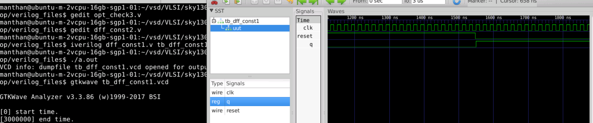
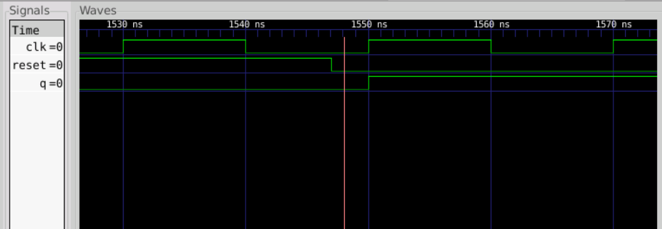
We observe that even after rst has become low Q waits for rising edge of the clock to go high. This circuit will infer a flop.
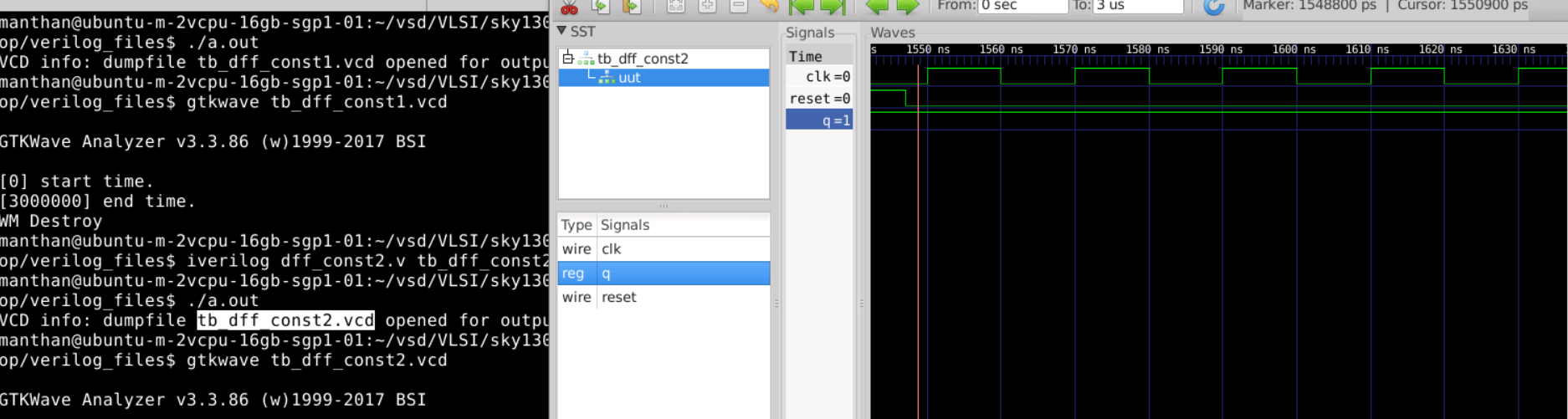
Now we Compare it with dff_const2.v
We see that Q does not depend upon clk unlike in the case of dff_const1.v
Now let us Synthesis both the files
As this is a sequential circuit while synthesis we have to give one more command dfflipmap for proper mapping of sequential cells in the library.
For dff_const1.v
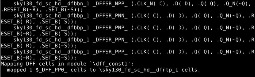
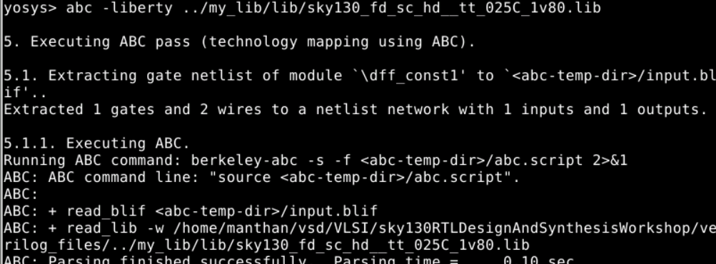
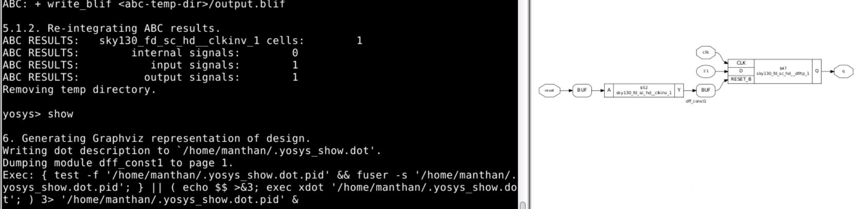
We get the following logic design
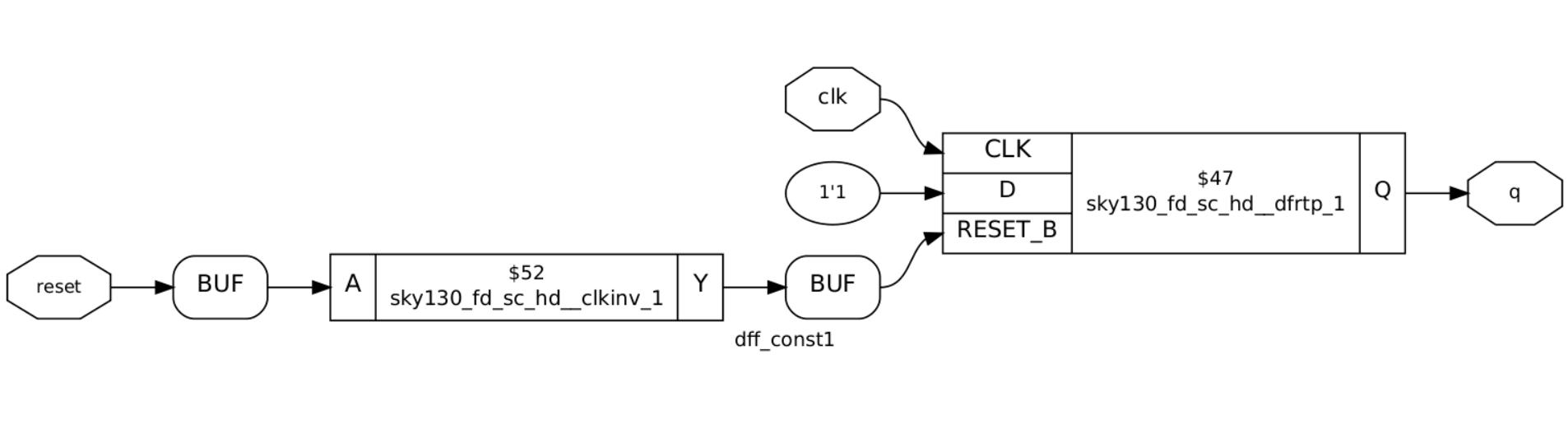
The standard cell library is expecting the reset to be active low but we have coded a active high reset so the tool is inferring a inverter.
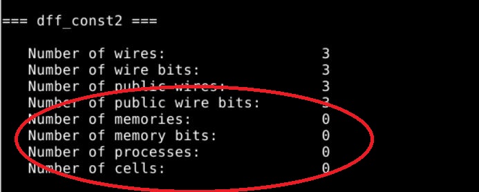
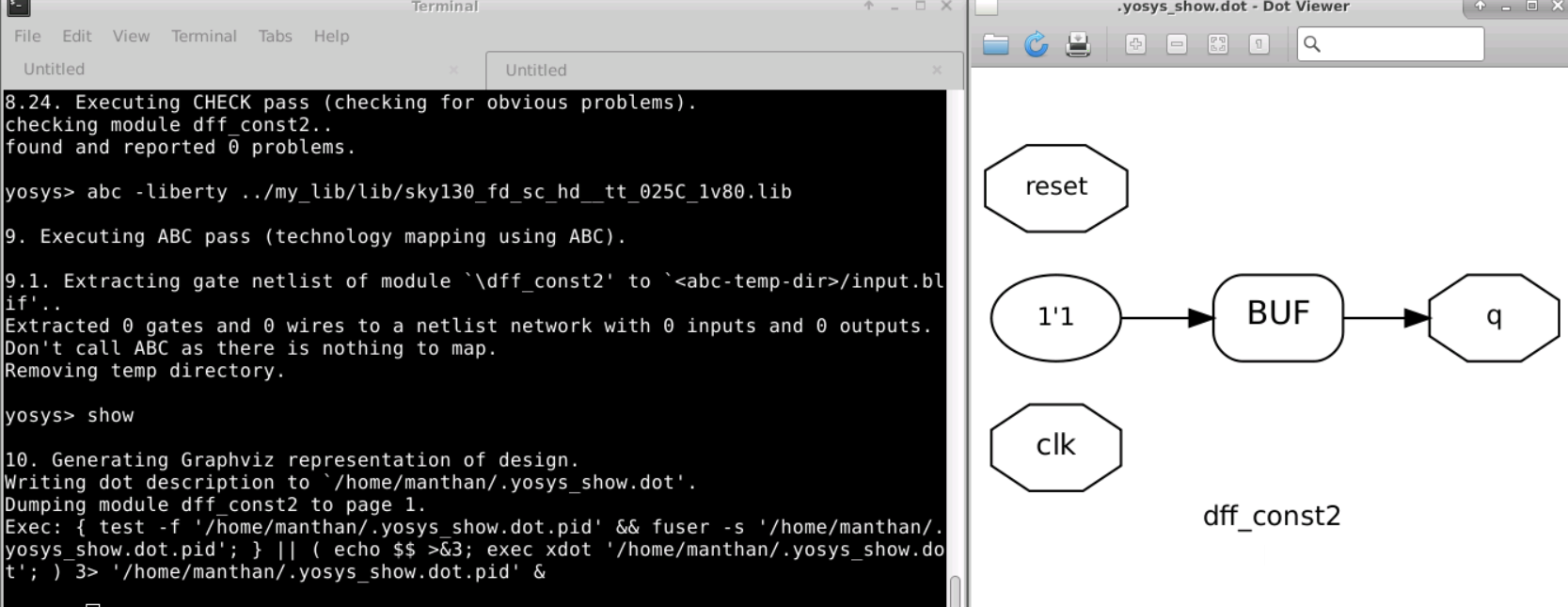
Now we synthesis dff_const2.v file
We observe that it has not inferred any flop in this case contradictory to dff_const2.v
Now let us take dff_const.v file
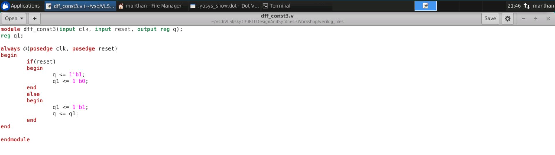
By observing the code we see that Q1 and Q both cannot be optimized so both the flops will be present in the Circuit.
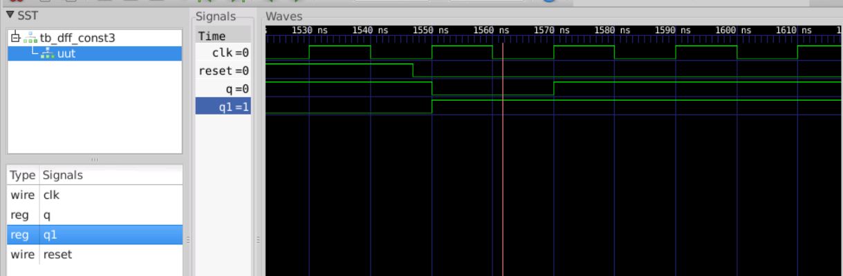
So first let us simulate our design

We can clearly see that both q and q1 do not remain constant and both change on the rising edge of the clock so the cannot be optimized
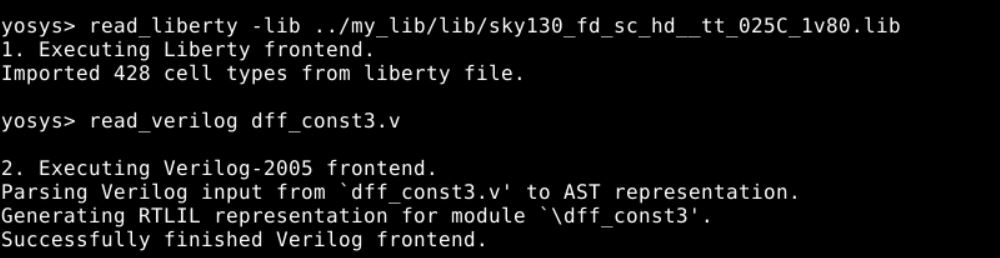
Now let us go ahead and do the synthesis of the circuit
We can clearly see it infers 2 flops
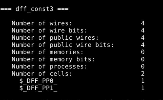
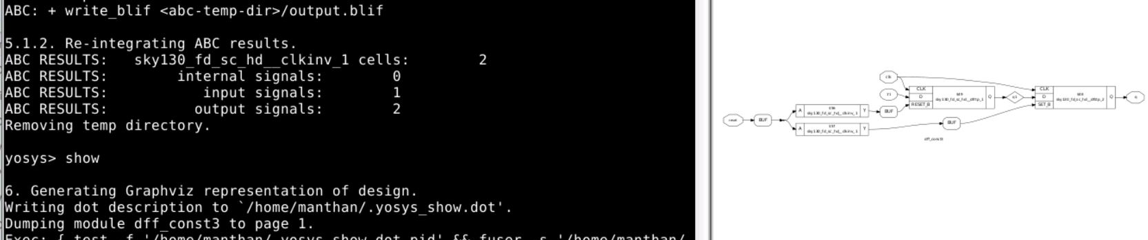
From the Logic diagram we have confirmed that 2 flops and also the 1st flop is a reset flop and the 2nd flop is a set flop.
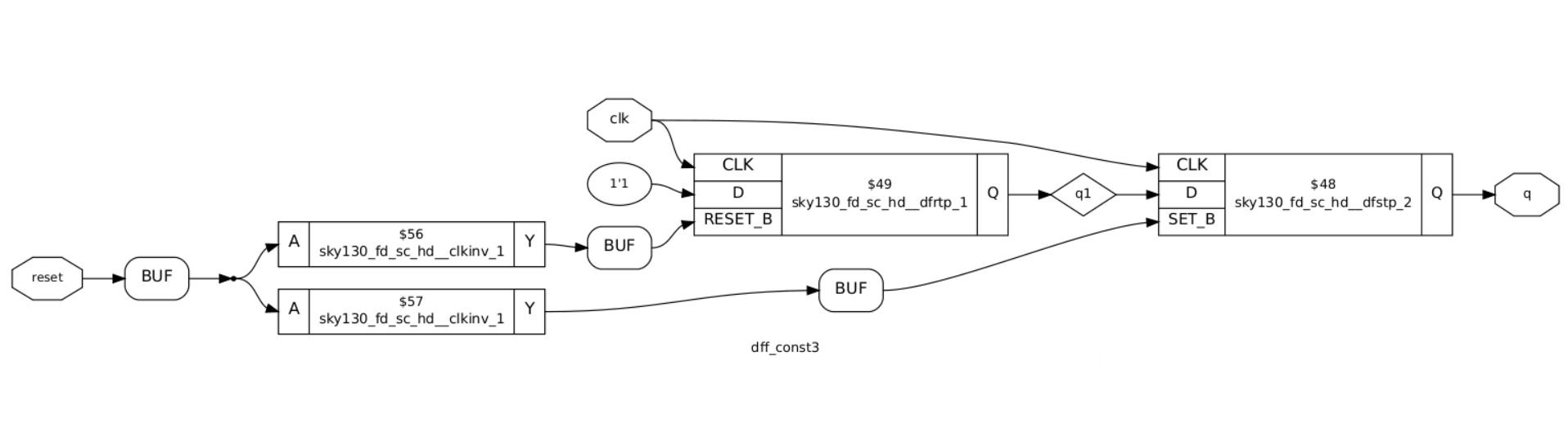
Not every flop which is having constant at the input gets optimized we also need to look at set and the reset connections and see if q is constant or q values is going to change.\
Lab3
Sequential Optimisation using Unused Output optimisation.
So let us consider the code counter_opt.v
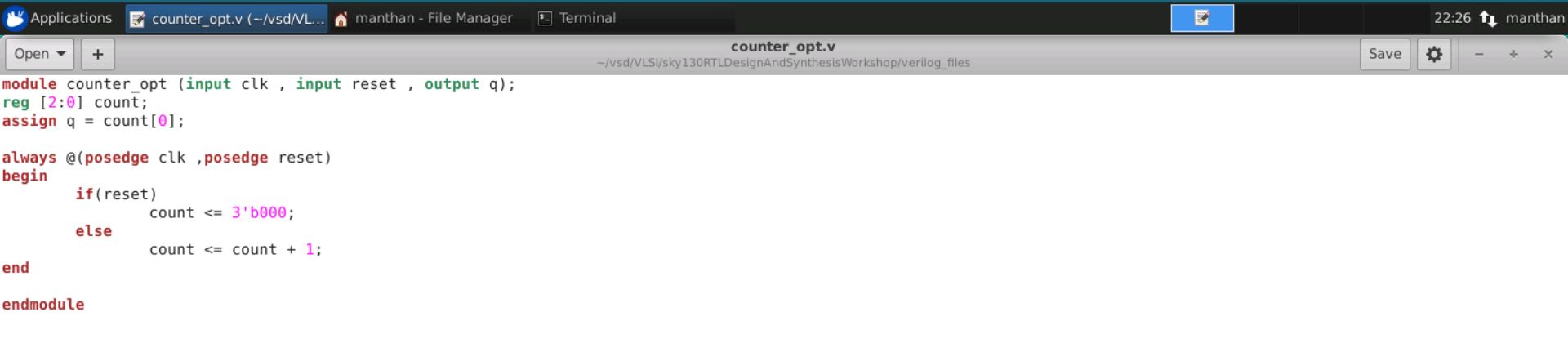
When we look at code we see that it is a up-counter whenever there is reset it reset otherwise its 3 bit up-counter.
The output of the circuit is count[2:0] but q = count[0]. count[1] and count[2] are unused. So this are not required in the logic diagram.
Let us synthesis this code.
We clearly see only 1 flop is inferred even if it is 3 bit counter it should have inferred 3 flops
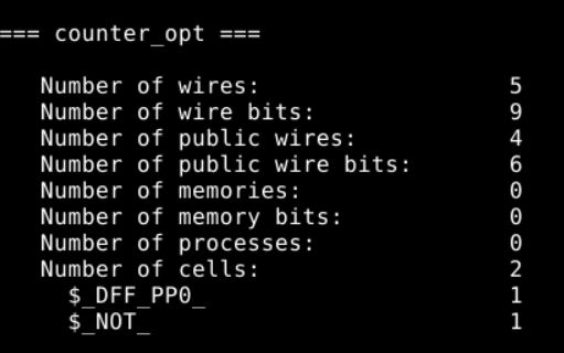
As it is a sequential circuit we should use dfflibmap -liberty ../my_lib/lib/<location of .lib file>

We can clearly see that there is only 1 flop in the circuit design.We see count[0] is toggling so the output q is given to the inverter and feededback to the d pin.
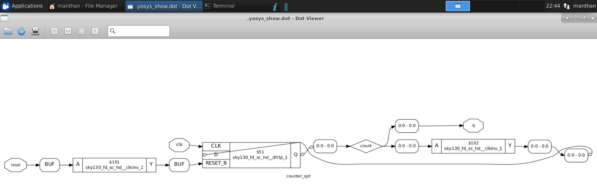
So we can conclude that any logic which is not resulting in any primary output is optimised away.
Now let us consider count_opt2.v
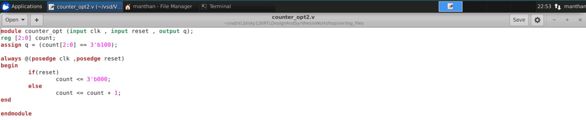
We have tweaked the code slightly from count_opt.v as we have changed assign q = (count[2:0] == 3'b100);
Now we expect that as all outputs are used it should have 3 flops to be present in the logic circuit.
Let us synthesis the code.
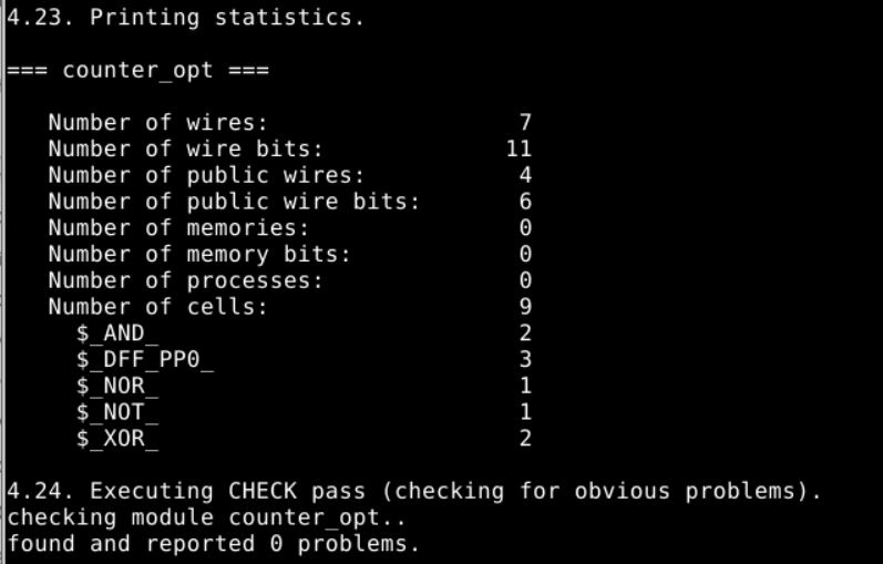
From the Figure above we clearly see that 3 flops are inferred here.
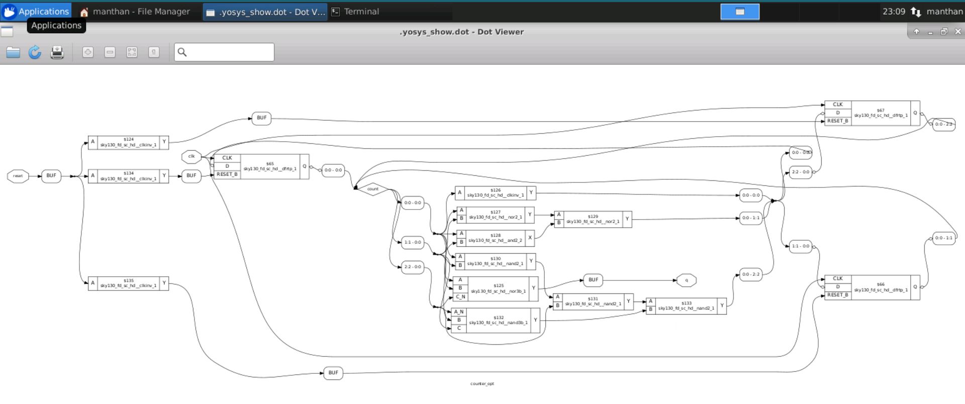
The logic other than the flops is the incremental logic.
The given Logic diagram contains 3 flops .We get the expression of q = count[2] . count[1]'.count[0]' so it is using all the primary outputs so it uses all the flops.
So we conclude that all the outputs that have no role in determining the primary output are optimized away using Unused Output Optimisation.
- It stands for Gate Level Simulation.
- Running the Test Bench With Netlist as design under Test.
- Netlist is logically same as the RTL Code.
- Same testbench will align with the design.
- Verify the LOgical Correctness of the design after synthesis.
- Ensuring the Timing of design is met
- For this GLS needs to be run with delay annotation.
- We give the Netlist,Gate Level Verilog Models and Testbench to the iverilog.
- Netlist has all the standard cell instantiated and the meaning of standard cell is conveyed to the iverilog by Gate Level Verilog Models.
- After which it has the same flow giving the vcd file using which we can generate Waveform using GTKwave.
Note
If the gate level models are delay annotated, then we can use GLS for timing validation.
-Suppose we have a Netlist
- and u_and(.a(a),.b(b))
- or u_or (.a(a),.b(b))
- Now to understand this we Gate level Verilog Models.They can
- Timing Aware -->validate functionality + timing both
- Functional --> validate functionality
- Missing Sensitivity List
- Blocking Vs Non-Blocking Assignments
- Non Standard verilog Coding
Let us consider a verilog Code
module mux(
input i0,input i1
input sel,
output reg y
);
always @ (sel)
begin
   if (sel)
            y = i1;
   else
            y = i0;

end
endmodule- Simulator works based on activity i.e the output will change only when there is a change in the input.
- In the Code given the always block is evaluating only when the sel is changing. As the always block is not sensitive to the changes in i0 and i1.
- Only when there is a change in sel the always block gets evaluated.
- When we simulate it acts as a latch.But when we synthesis it will act as a Mux.
- This is called missing elements of sensitivity list.
- Now let us consider another code
module mux(
input i0,input i1
input sel,
output reg y
);
always @ (*)
begin
   if (sel)
            y = i1;
   else
            y = i0;

end
endmodule- In this case always is evaluated when any signal changes.
- So now always block will be evaluated for i1 as well as i0
- This will simulate as Mux and also be synthesised as Mux.
- Inside always block
- If we are using '=' to make assignments
- Executes the Statement in the order it is written.
- So the first statement is evaluated before the second statement.
- If we are using '<=' to make assignments
- Executes all the RHS when always block is enteredand assigns to LHS
- Parallel Evaluation
- If we are using '=' to make assignments
- Let try to create a shift register
module code (input clk,input reset,
input d,
output reg q);
always @ (posedge clk,posedge reset)
begin
if(reset)
begin
        q0 = 1'b0;
        q = 1'b0;
end
else
        q = q0;
        q0 = d;

end
endmodule- In this case q0 is assigned to q and then d gets assigned to q0.So we get 2 values.
- So it has 2 flops.
- Now let change the code slightly
module code (input clk,input reset,
input d,
output reg q);
always @ (posedge clk,posedge reset)
begin
if(reset)
begin
        q0 = 1'b0;
        q = 1'b0;
end
else
        q0 = d;
        q = q0;

end
endmodule- In this case q0 is assigned d the q0 gets assigned to q
- So it is as if q is getting the value of d which means it only has 1 flop
- But if we write it with non blocking statements
module code (input clk,input reset,
input d,
output reg q);
always @ (posedge clk,posedge reset)
begin
if(reset)
begin
        q0 <= 1'b0;
        q <= 1'b0;
end
else
        q0 <= d;
        q <= q0;

end
endmodule
- So we conclude that non blocking statements should be used to write Sequential Circuit Code.
Now Let us look at another code.
Our aim is to create a circuit with output as y = (a + b).c
module code (input a,b,c
output reg y);
reg q0;
always @ (*)
begin
        y = q0 & c;
        q0 = a|b ;

end
endmodule- We assign the value of y with q0 and with c first and then assign q0 as a or b
- So we see that q0 value is the old q0 value and is not updated.
- When we simulate old q0 value will mimic a delay or flop but when we synthesis there will not be a flop.
- Now let us change the order of block statement
module code (input a,b,c
output reg y);
reg q0;
always @ (*)
begin
        q0 = a|b ;
        y = q0 & c;


end
endmodule- In this case there will not be any delay as the q0 is updated first then used.
- When we simulate it will work as the given circuit.
- In both cases above when we synthesis we get the desired circuit but in first case the simulation result differ with synthesis results.
Because of these kind of issues it becomes very important to run GLS on the Netlist and match with the expected output and see if there are no Synthesis Simulation Mismatches.
LAB Session
Lab 1
In this Session we are going to see how to invoke GLS and run some basic experiments with GLS.
To Run GLS we need
- Netlist
- Verilog Models
- Testbench
Let us consider the file ternary_operator_mux.v
- Ternary Operator
<cond> ? <T>:<F>- If the condition is true the 'T' part is executed and if it is false 'F' part is executed.
Now let us have a look at the code of ternary_operator_mux.v

The code given is basically a Mux implemented using a ternary operator.
Now let us first do the RTL simulation.
For that we first invoke iverilog and then execute the a.out file using ./a.out
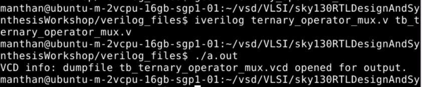
After getting the vcd file use gtkwave <file name> to see the simulation.
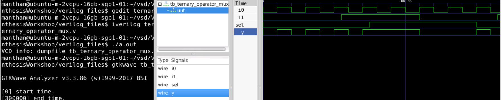
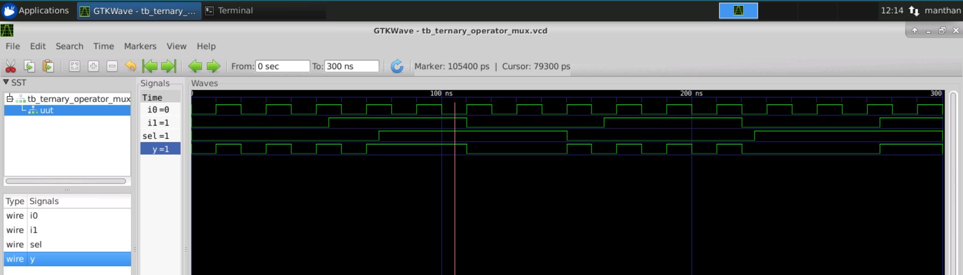
Here we observe it is clearly following the behaviour of 2:1 MUX.
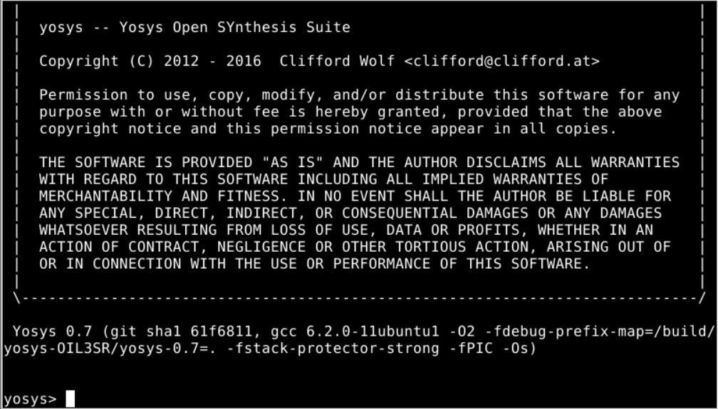
Step 1 : Now let us systhesis for which we invoke yosys
Step 2 : To Load the .lib file we use the command read_liberty -lib ../my_lib/lib/...

Step 3 : Then we read the verilog file using read_verilog <file name>

Step 4 : Now let us start the synthesis process using synth -top <file name>
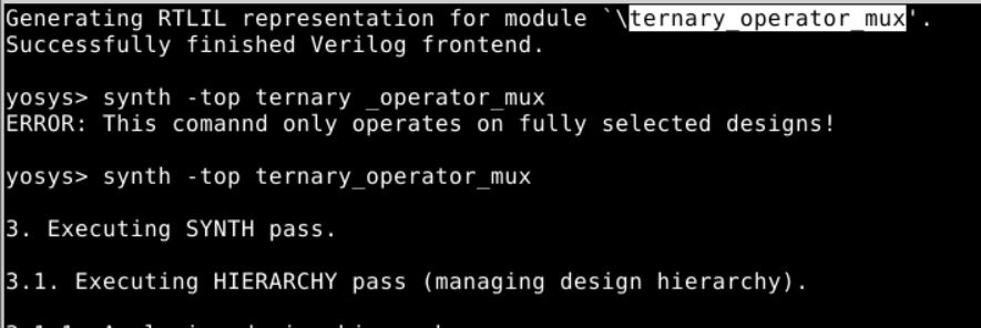
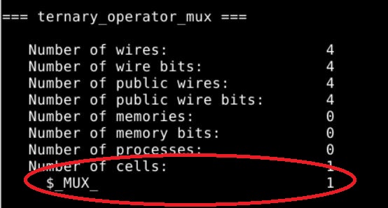
We can clearly see that 1 Mux has been infered.
Step 5 : Now let us use the abc -liberty ../my_lib/lib/<.lib file>
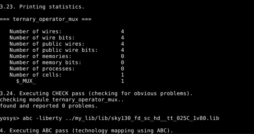
Step 6 : and then use show to get the logic diagram generated.

This is the Logic Diagram generated
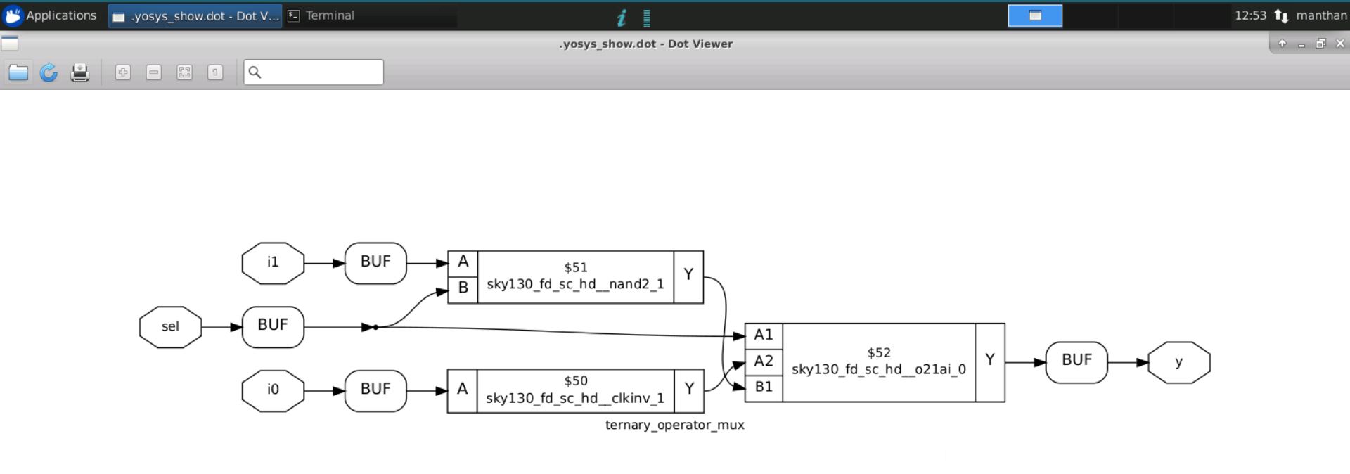
If we Solve the logic diagram we get the result as y = sel .i1 + sel'.i0.Exactly
Now let us do the GLS.
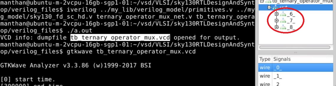
Step 1 : Open iverilog with verilog models,netlist, and testbench using the command iverilog. In the lib folder you will find the verilog models of the standard cells.Execute a.out file using ./a.out

Step 2 : Now as the vcd file is generated.Now we use GTKwave to observe the simulation by giving the command gtkwave

We know the difference GLS and RTL as in GLS under uut there no files but in GLS we 6 , 7 , 8.
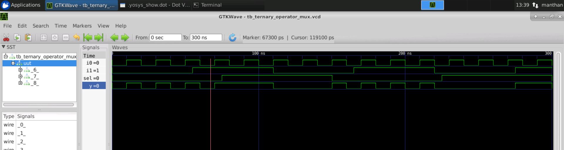
Now let us observe the simulation. It is clearly following the MUX output.
Now Let us take another example of bad_mux.v

We can observe that in this case the always block going to be evaluated only upon changes in sel.
So in simulation it we work as some kind of flop.
Now let us carry out the RTL simulation using the steps we followed for simultion above
Let us observe the simulation results by giving the command gtkwave
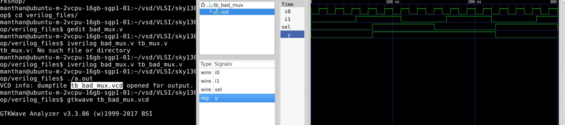
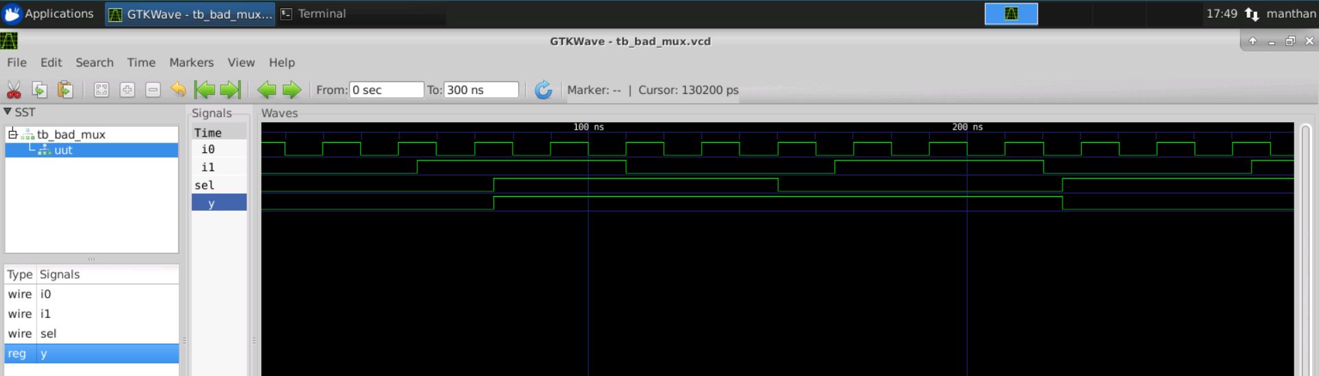
So we can observe that if there is no activity on the output does not change.
This simulation shows as if the Mux is acting like a flop .
Now let us synthesis and see what happens.
Step 1 : For synthesis we invoke yosys
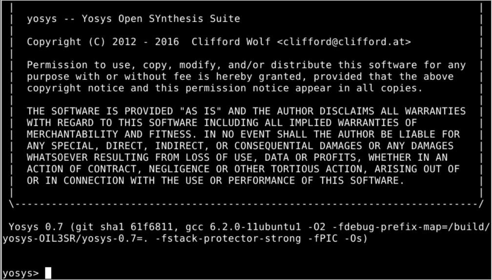
Step 2 : To Load the .lib file we use the command read_liberty -lib ../my_lib/lib/...
Step 3 : Then we read the verilog file using read_verilog <file name>
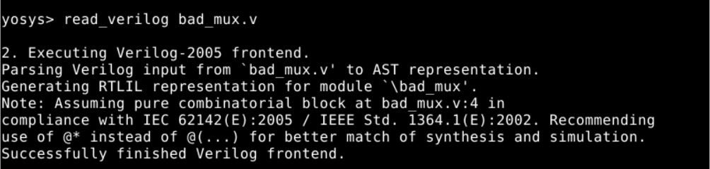
Step 4 : Now let us start the synthesis process using synth -top <file name>
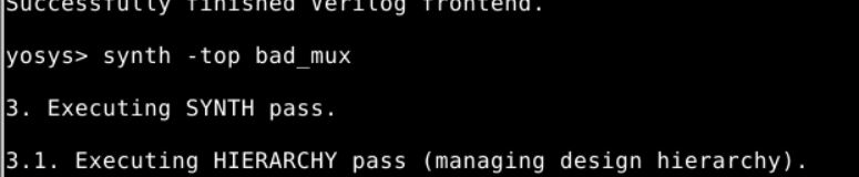
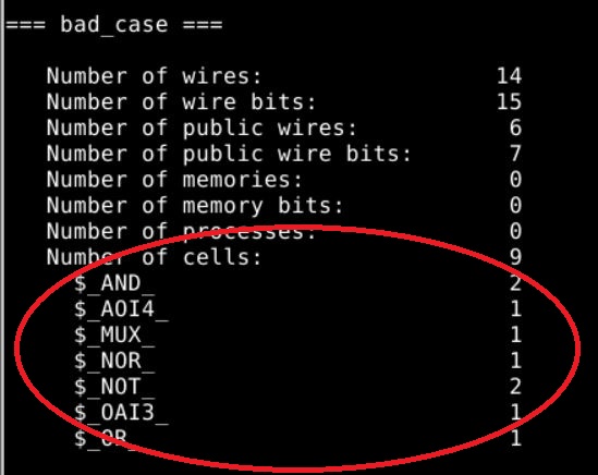
Here are some details of which gates are inferred
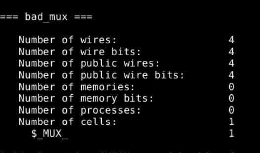
So we see it infers MUX not a latch.
Step 5 : Now let us use the abc -liberty ../my_lib/lib/<.lib file>
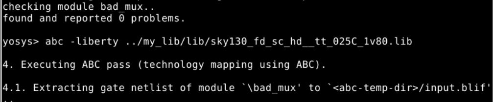
Step 6 : Now to get the netlist file we use write_verilog
Now let us do the GLS.
Step 1 : For that we need to open iverilog with verilog models,netlist, and testbench using the command iverilog. In the lib folder you will find the verilog models of the standard cells.Execute a.out file using ./a.out

Step 2 : Now we use GTKwave to observe the simulation by giving the command gtkwave

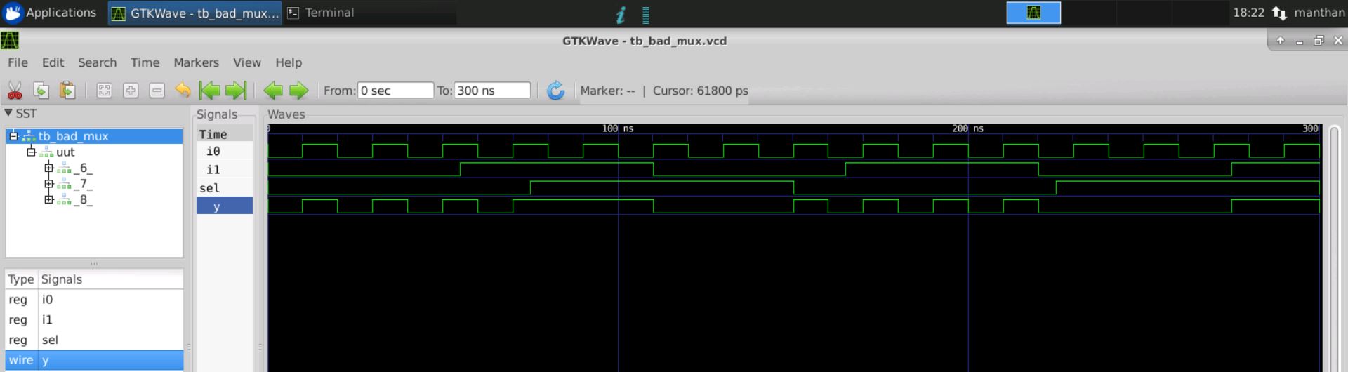
Now we compare the simultion with the RTL design and after synthesis Netlist simulation.
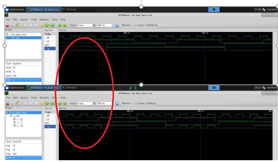
In the GLS simulation the activity on i1, i0 has been reflected on output whereas in the RTL simulation the output was effected by only the sel.
This is called Synthesis Simulation Mismatch.
Lab2
In this Lab we will continue to see the Synthesis Simulation Mismatch.
Now Let us take a blocking code example.

The aim of this code is to get the d = (a+b).c
Now because of the blocking statement first d will be assigned (x and c) then x = a or b will be executed.
So by the time the statement for d is getting evaluated we have the previous value of x .
So when we simulate it , it will look as if x is a flopped output.
Now let us do the RTL simulation using the steps we followed for different simulations
Let us observe the simulation result by giving the command gtkwave
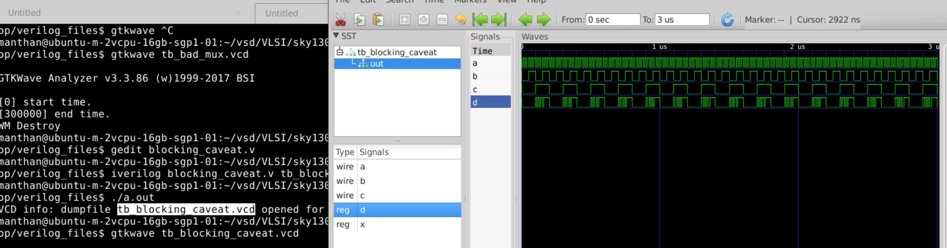
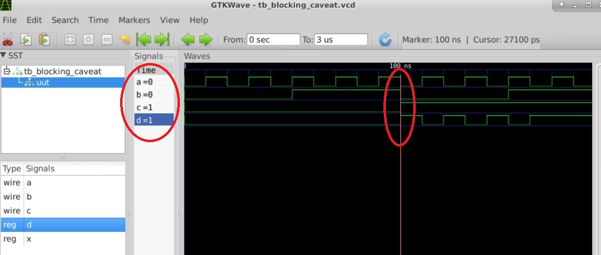
We see from the simulation that the value of d = 0 but it is coming out to be 1 because the past value of (a or b) is 1 in the cycle before that value is getting anded with the present value of c.
Now let us synthesis using the steps we followed in various examples above and see what happens.
After synth -top
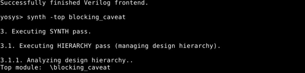
Here are some details of which gates are inferred
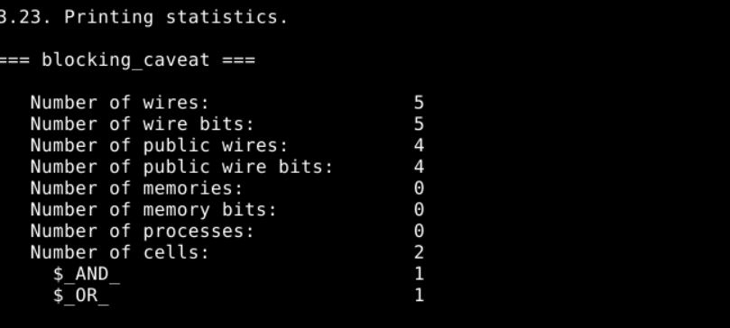
Step 6 : Now let us use the abc -liberty ../my_lib/lib/<.lib file>
Step 7 : Now to get the netlist file we use write_verilog

Before going to the GLS let us look at what logic we got by giving the command show.
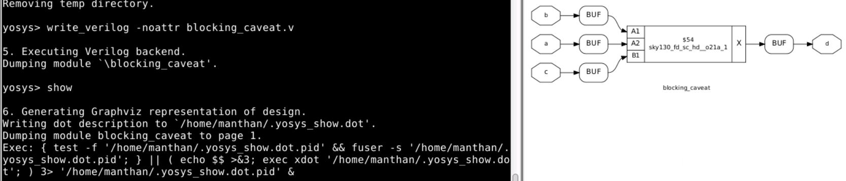
We clearly see that it is very straight forward with or 2 and gate used and no latches in the design.
Now let us do the GLS using the step we followed in above example
Let us observe the simulation results we got
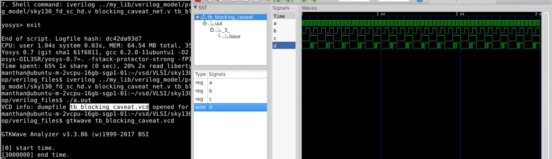
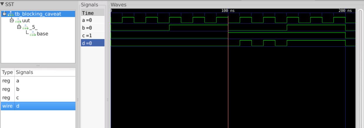
Now we compare the simultion with the RTL design and after synthesis Netlist simulation.
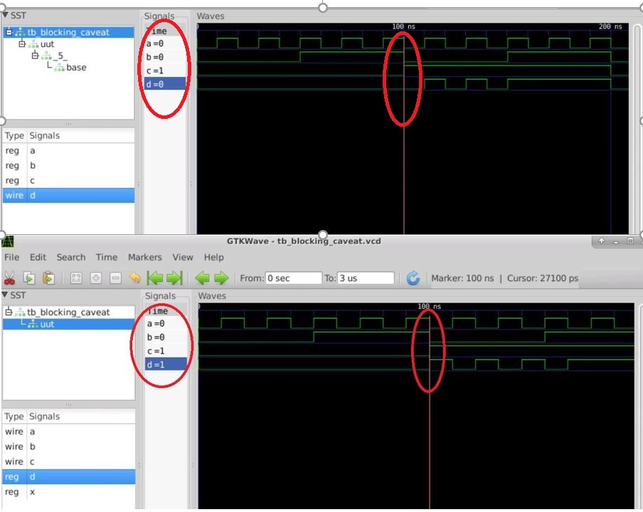
We can clearly see that the value of d = 0 for the same case where a = 0,b = 0 and c = 1.
This is Synthesis Simulation Mismatch caused by Blocking statement.
Note
Please be very carefull before using blocking statements for Sequential Circuits.
In this section we will study about if and case Statement and there uses as well as there disadvantages.
- if is basically a priority logic
if<cond>
begin
.....
.....
end
else
begin
.....
.....
end
and if-else statement
if<cond>
begin
.....
.....
end
else if<cond2>
begin
.....
.....
end
else if<cond3>
begin
.....
.....
end
else
begin
.....
.....
end
The Hardware Implementation of these statement is as shown in the image below.
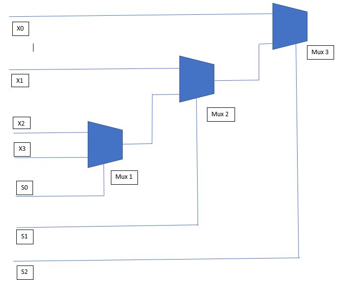
- inferred latches --> it is a bad coding style and occurs due to incomplete if statement
- Sometimes we need the inferred latch like in the case of counters if there is no enable the counter should latch on to the previous value.
Note
In Combinational Circuit we cannot have a inferred latch. Whatever variable you are trying to assign should be register variable.
- if and case statement are used inside the always block
reg y
always @ (*)
begin
	case(sel)
		2'b00:begin
		      ....
		      end
		2'b01:begin
		      ....
		      end
		      .
		      .
		      .
endcase - Hardware implementation of Case statement is a MUX.
- inferred latches --> it is a bad coding style and occurs due to incomplete case statements
- The solution for inferred latches is code Case with default condition
- With default condiation it avoids the inferred latches
LAB Session
Lab 1
In this session we will use the if statement and incomplete if statement.
We first take the code incom_if.v
module incomp_if (input i0 , input i1 , input i2 , output reg y);
always @ (*)
begin
	if(i0)
		y <= i1;
end
endmodule- We observe that in this code there is no else statement.
Now let simulate and synthesis it.
Step 1 : Useiverilogto generate the a.out file for simulation

Step 2 : Execute the a.out file to get the vcd file

Step 3 : Usegtkwaveto view the waveform of gcd file
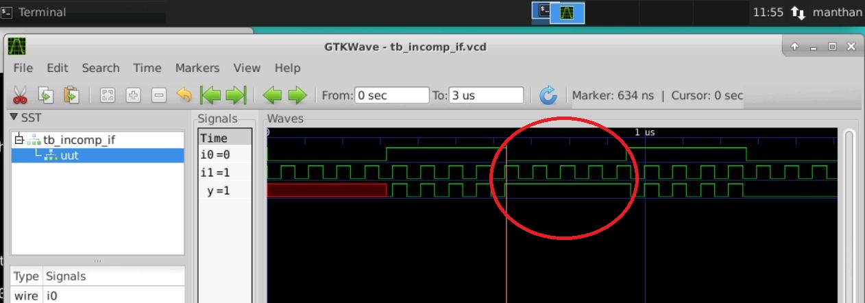
We observe that whenever i0 is low the value of y is latched as it is constant.
Now let us go for synthesis.
Step 1 : Invoke yosys usingyosys
Step 2 : Read liberty file usingread_liberty
Step 3 : Read verilog file usingread_verilog

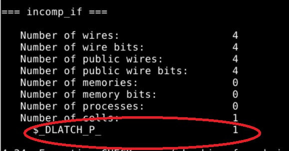
Step 4 : For starting the synthsis process usesynth -topand also observe the inferences
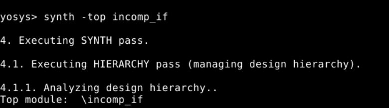
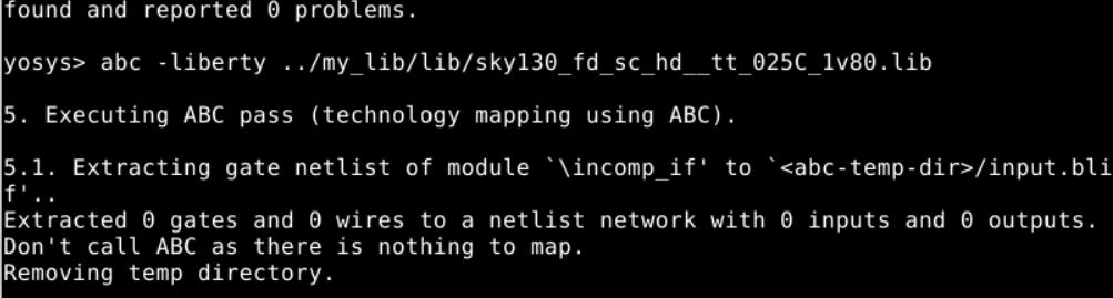
Step 5 : Now to map to standard cell we useabc -liberty
Step 6 : Now to see the Logic design we give the commandshow
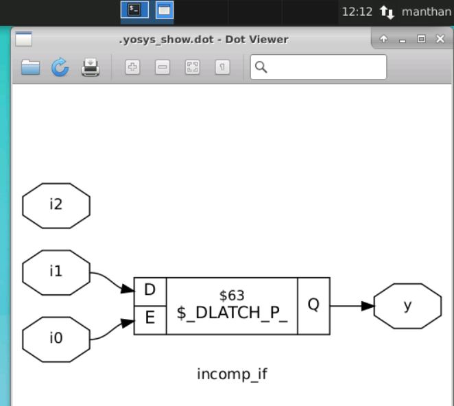
It is a D latch. This is the danger of incomplete if we get a latch instead of mux. This is called as inferred latch.
Lab 2
Now let us see the case statement and incomplete case statements.
We first take the code incom_if.v.
module incomp_case (input i0 , input i1 , input i2 , input [1:0] sel, output reg y);
always @ (*)
begin
	case(sel)
		2'b00 : y = i0;
		2'b01 : y = i1;
	endcase
end
endmodule- We observe that there is no case for when sel = 10 and 11.
Now let simulate and synthesis it.
Step 1 : Useiverilogto generate the a.out file for simulation

Step 2 : Execute the a.out file to get the vcd file

Step 3 : Usegtkwaveto view the waveform of gcd file
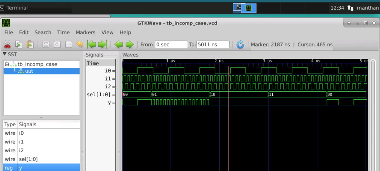
When the Value of sel = 10 and 11 it latches on to the value of previous state.
Now let us go for synthesis.
Step 1 : Invoke yosys usingyosys
Step 2 : Read liberty file usingread_liberty
Step 3 : Read verilog file usingread_verilog

Step 4 : For starting the synthsis process usesynth -topand also observe the inferences
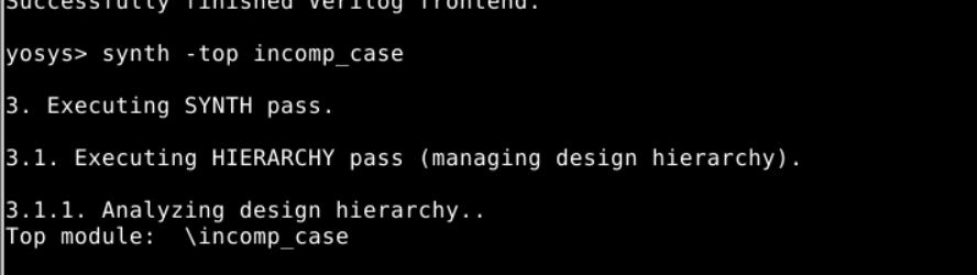
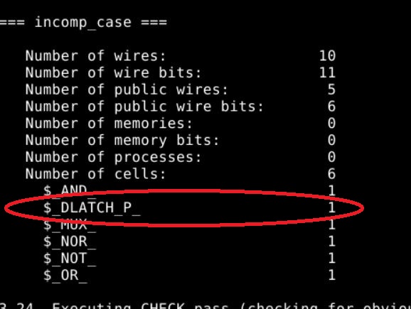
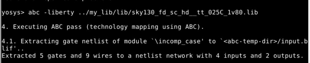
Step 5 : Now to map to standard cell we useabc -liberty
Step 6 : Now to see the Logic design we give the commandshow
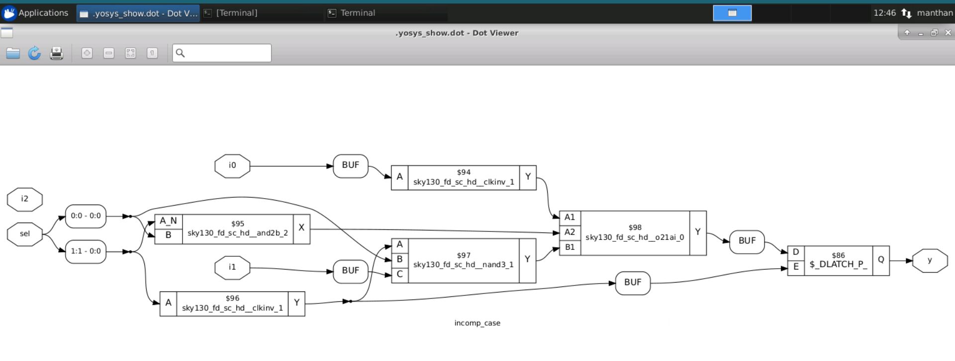
There is a D latch in the circuit.This is the danger of incomplete case we get a latch instead of mux. This is called as inferred latch.
If we consider the comp_case.v
module comp_case (input i0 , input i1 , input i2 , input [1:0] sel, output reg y);
always @ (*)
begin
	case(sel)
		2'b00 : y = i0;
		2'b01 : y = i1;
		default : y = i2;
	endcase
end
endmodule- As there is a default statement there will be no latch involved in this design.
Now let simulate and synthesis it using the same steps above and conclude our finding.
After Simulation we get the following waveform
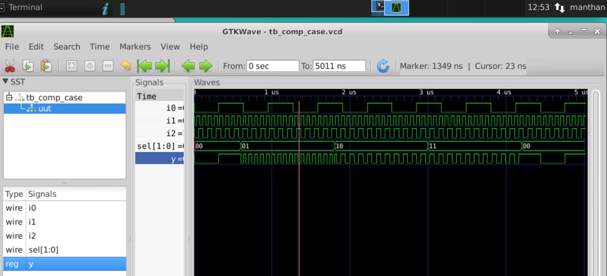
This waveform clearly suggest that there is no latch involved and it a pure MUX circuit.
After Synthesis we get the following design
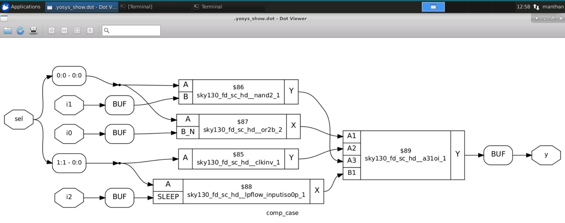
- Clearly we can see there is latching action when sel = 10 and 11 the output is i2.
If we consider the partial_case_assign.v
module partial_case_assign (input i0 , input i1 , input i2 , input [1:0] sel, output reg y , output reg x);
always @ (*)
begin
	case(sel)
		2'b00 : begin
			y = i0;
			x = i2;
			end
		2'b01 : y = i1;
		default : begin
		           x = i1;
			   y = i2;
			  end
	endcase
end
endmodule-
Even if assign default statement it does not gurantee that latches are not inferred. Now let synthesis it using the same steps above and conclude our finding.
After Synthesis we get the following design
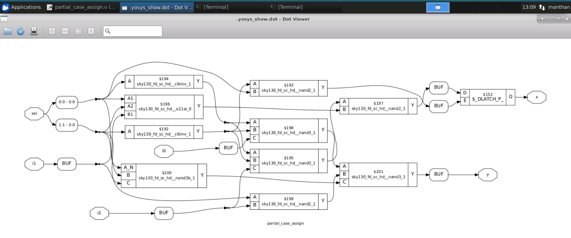
-
Clearly we see there no latch in the path of x but in the path of y there is latch as condition for 01 is not defined. If we consider bad_case.v
module bad_case (input i0 , input i1, input i2, input i3 , input [1:0] sel, output reg y);
always @(*)
begin
	case(sel)
		2'b00: y = i0;
		2'b01: y = i1;
		2'b10: y = i2;
		2'b1?: y = i3;
		//2'b11: y = i3;
	endcase
end

endmodule- In this case for sel = 11 there are 2 options available i.e y=i2 and y=i3 this will cause some issue while simulating and synthesising it.
Now let us simulate and synthesis it using the same steps above and conclude our finding.
After Simulation we get the following waveform
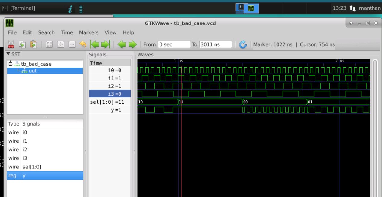
The waveform clearly suggests that when sel = 11 it is getting confused and latching on to the value '1'as both condition 10 and 11 both are matching.
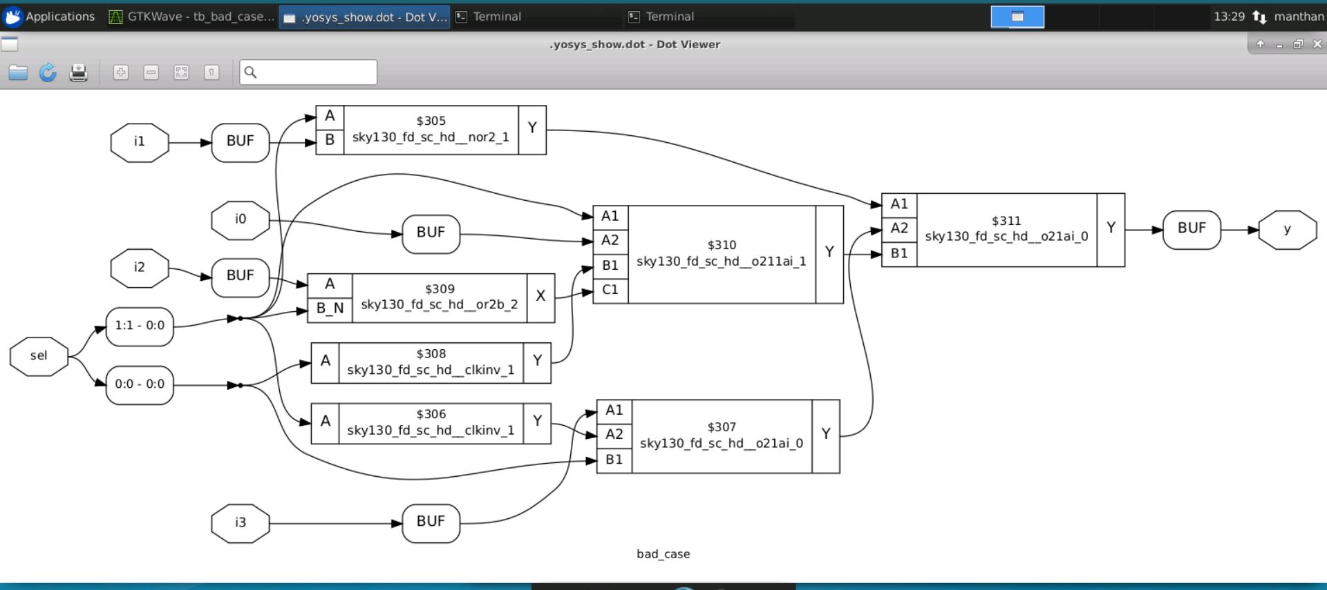
After Synthesis we get the following design
No latch inferred for the design
Now Let us do the GLS
Step 1 : Usewrite_verilogto the netlist
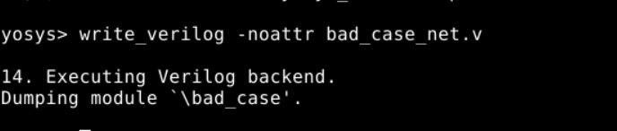
Step 2 : Open iverilog with verilog models,netlist and testbench using the commandiverilog. In the lib folder you will find the verilog models of the standard cells.Execute a.out file using./a.out

Step 3 : Now we use GTKwave to observe the simulation by giving the commandgtkwave
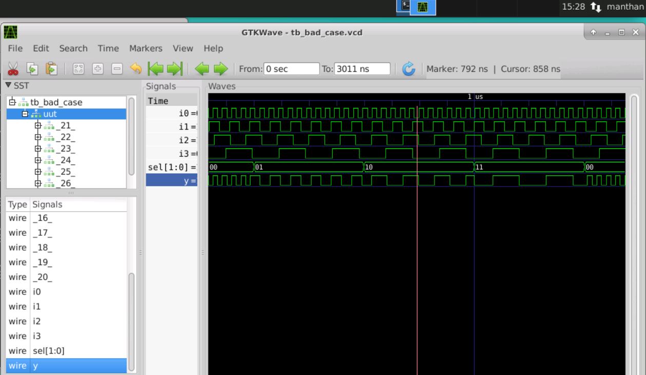
- We can clearly see that in this wave form it is not getting confused and when sel = 11 it follows i3.
There are 2 types of loops
- For Loop
- Used inside always block.
- Used for evaluating expressions.
- Not used for instantiating hardware.
- Generate For Loop
- Used outside always block.
- Cannot be used inside always
- Used for instantiating hardware
Lab 3
Let us understand the for statement with the use of some examples.
Let us consider mux_generate.v
module mux_generate (input i0 , input i1, input i2 , input i3 , input [1:0] sel  , output reg y);
wire [3:0] i_int;
assign i_int = {i3,i2,i1,i0};
integer k;
always @ (*)
begin
for(k = 0; k < 4; k=k+1) begin
	if(k == sel)
		y = i_int[k];
end
end
endmodule
Now let simulate it using the same steps above
After Simulation we get the following waveform
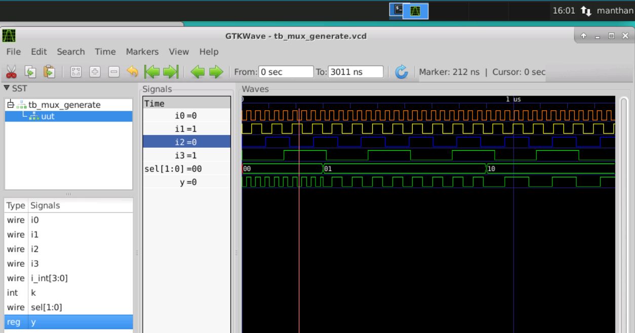
- It is clearly behaving as a 4x1 Mux.If we write the same code using case statement the code and the value of mux input is increased the gets too complicated but using the for statement we are able to write it easily.
Now let us consider demux_case.v and demux_generate.v and compare them
demux_case.v
module demux_case (output o0 , output o1, output o2 , output o3, output o4, output o5, output o6 , output o7 , input [2:0] sel  , input i);
reg [7:0]y_int;
assign {o7,o6,o5,o4,o3,o2,o1,o0} = y_int;
integer k;
always @ (*)
begin
y_int = 8'b0;
	case(sel)
		3'b000 : y_int[0] = i;
		3'b001 : y_int[1] = i;
		3'b010 : y_int[2] = i;
		3'b011 : y_int[3] = i;
		3'b100 : y_int[4] = i;
		3'b101 : y_int[5] = i;
		3'b110 : y_int[6] = i;
		3'b111 : y_int[7] = i;
	endcase

end
endmodule
demux_generate.v
module demux_generate (output o0 , output o1, output o2 , output o3, output o4, output o5, output o6 , output o7 , input [2:0] sel  , input i);
reg [7:0]y_int;
assign {o7,o6,o5,o4,o3,o2,o1,o0} = y_int;
integer k;
always @ (*)
begin
y_int = 8'b0;
for(k = 0; k < 8; k++) begin
	if(k == sel)
		y_int[k] = i;
end
end
endmodule- We observe that demux_generate.v is using for statement because of which the the lenght of the code is decreased.
Now let simulate demux_case.v using the same steps above
After Simulation we get the following waveform
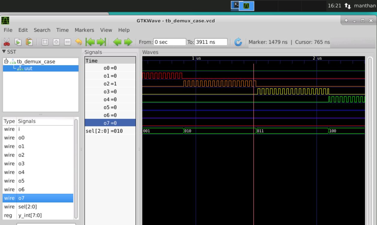
- We clearly observe from the wave the when sel = 1 o1 follows the input ,sel = 2 o2 follows the input and so on it clearly behaves as 1:8 demux.
Now let simulate demux_generate.v using the same steps above
After Simulation we get the following waveform
After Simulation we get the following waveform
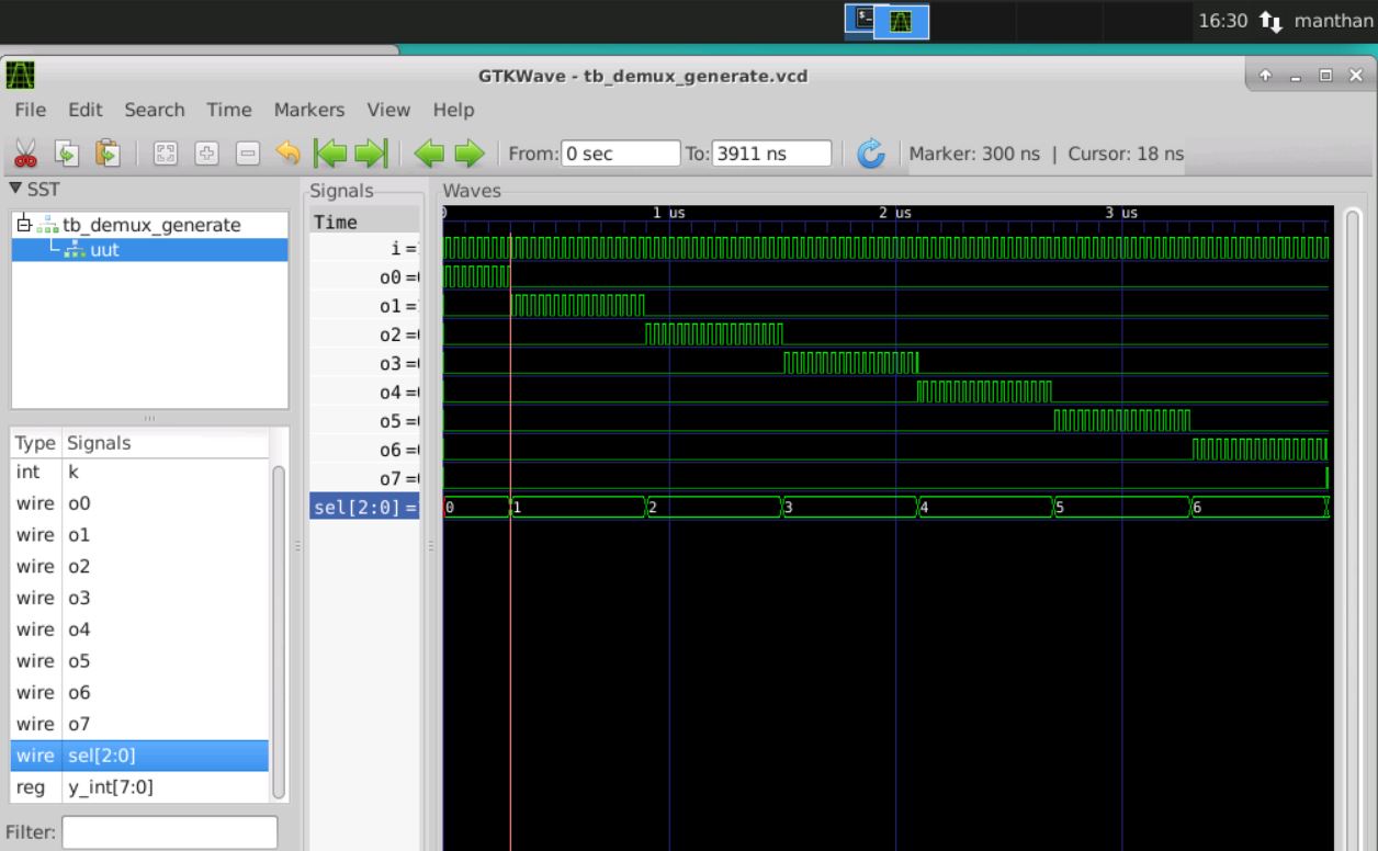
- Both the Waveforms are exactly the same the difference is just in the coding.
- demux_generate.v is more elegant code than demux_case.v
Let us understand the for generate statement with the use of some examples.
So Let us consider rca.v and fa.v
rca.v
module rca (input [7:0] num1 , input [7:0] num2 , output [8:0] sum);
wire [7:0] int_sum;
wire [7:0]int_co;

genvar i;
generate
	for (i = 1 ; i < 8; i=i+1) begin
		fa u_fa_1 (.a(num1[i]),.b(num2[i]),.c(int_co[i-1]),.co(int_co[i]),.sum(int_sum[i]));
	end

endgenerate
fa u_fa_0 (.a(num1[0]),.b(num2[0]),.c(1'b0),.co(int_co[0]),.sum(int_sum[0]));


assign sum[7:0] = int_sum;
assign sum[8] = int_co[7];
endmodule
fa.v
module fa (input a , input b , input c, output co , output sum);
	assign {co,sum}  = a + b + c ;
endmodule- There is no always block used in thesen codes.
- The variable we used here is called the genvar not an integer.
Note
Rules for addition
- N and N bit number --> Sum will be N+1 bit
- N and M bit number --> Sum will be Max(N,M)+1 bit
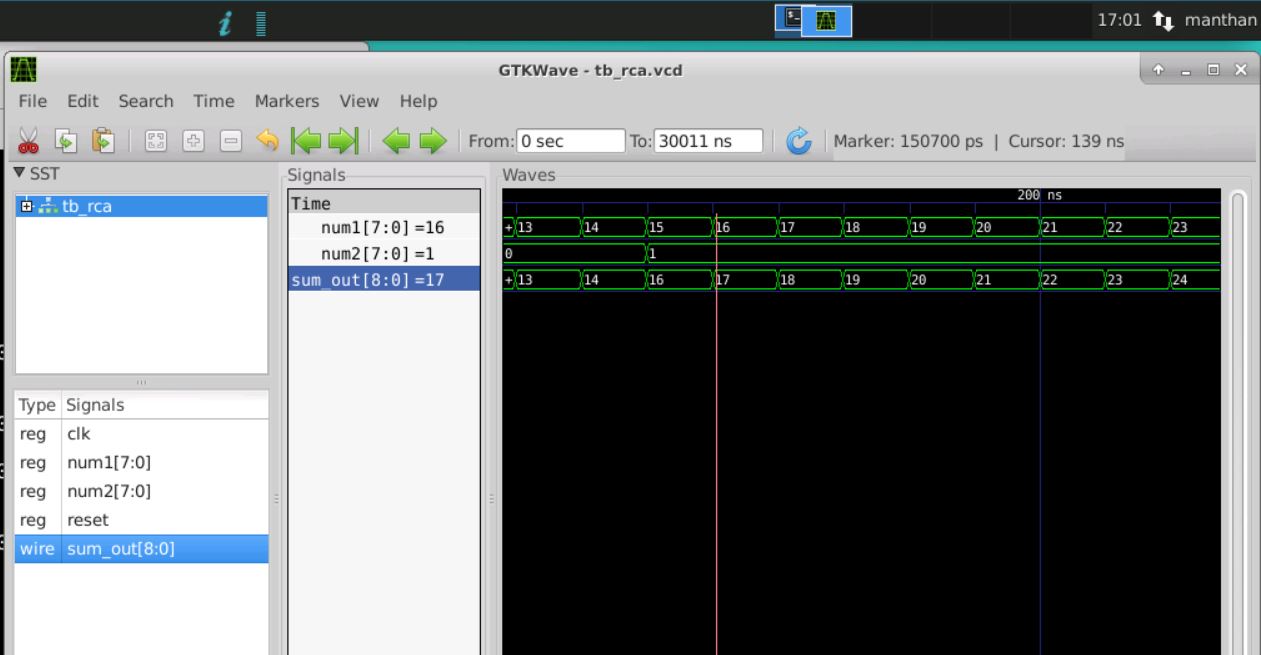
Now let simulate using the step followed above. In this case before compiling rca.v we call fa.v to specify where the defination of fa is present.

After Simulation we get the following waveform
Some of the observations made during the lab session and group discussion of the workshop
-
While reading the library file if we miss the keyword
-libwe get this kind of error
- So we conclude that
-libkeyword is used for identifying logic operations
-
In the synthesis process if we do not map it to standard cell using
abc -libertyand instead give the commandshow- for example take ternary_operator_mux.v
- without abc command and directly
showwe get 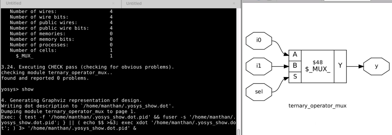
- with abc command and then
showwe get 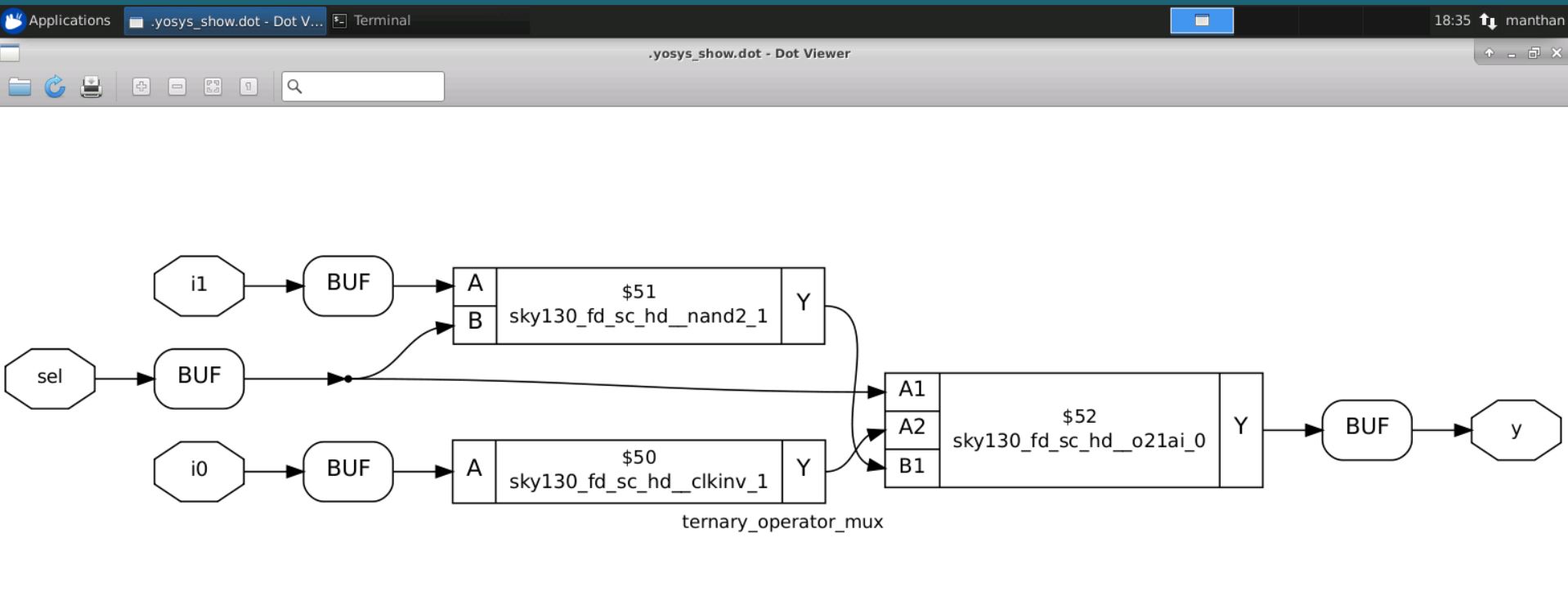
- So we conclude that abc links the module to the basic logic gate using which it the module is formed.
-
When we want to see the netlist we open the _net.v file
-
write_verilog -noattr < _net.v file_name>after which if we read the file usinggeditwe get the netlist file- if we do not write
-noattrwe get a small difference 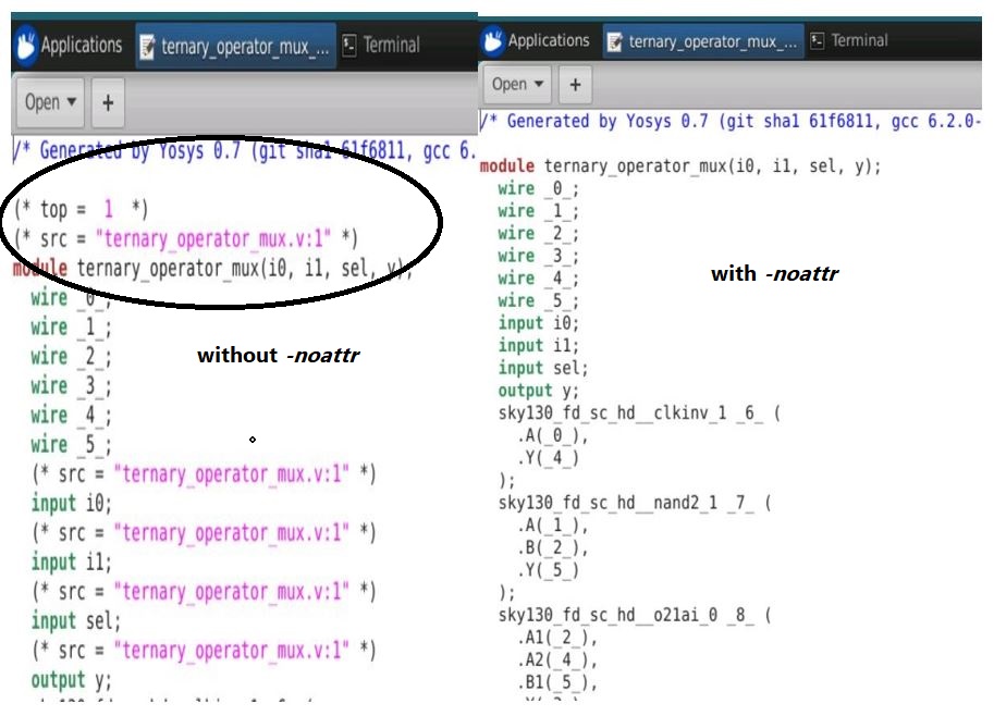
- if we do not write
-
dfflibmapis used to map the sequential circuit codes with standard cell library file -
Every new version of the yosys tool comes with its own optimization techniques.So many times the implementations will differ in dfferent version.