Main Important Coding Styles of Verilog
In Verilog, a behavioral model is a high-level description of a digital circuit that describes its function and behavior using a set of algorithms or equations. It is often used to create an initial design that can be refined and optimized at a later stage. Behavioral models describe the function of a digital circuit without specifying the underlying hardware components or implementation details.
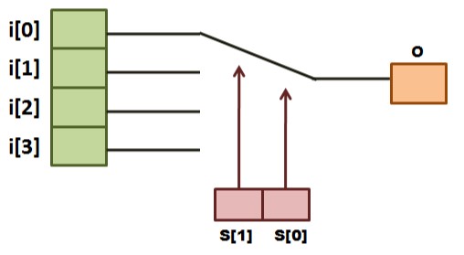
module Mux_4_1(input [3:0] i,input [1:0] s,output reg o);
always @(s or i)
begin
case (s)
  2'b00 : o = i[0];
  2'b01 : o = i[1];
  2'b10 : o = i[2];
  2'b11 : o = i[3];
  default : o = 1'bx;
endcase
end
endmodule
The dataflow model in Verilog is a style of digital circuit modeling that describes how signals flow through a circuit. In the dataflow model, Verilog code is written using a set of equations that describe the logical relationships between inputs and outputs.
The designer specifies the behavior of the circuit in terms of the data flow, rather than the explicit sequence of operations that should be performed to generate the output.
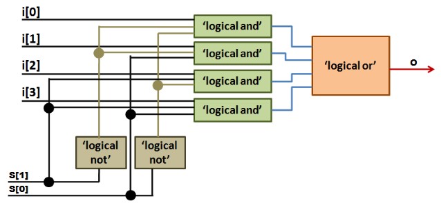
 module Mux_4_1_df(input [3:0] i,input [1:0] s,output o);
 assign o = (~s[1] & ~s[0] & i[0]) | (~s[1] & s[0] & i[1]) | (s[1] & ~s[0] & i[2]) | (s[1] & s[0] & i[3]);
 endmodule
The gate-level model in Verilog is a low-level digital circuit modeling style that describes the circuit using a collection of logic gates and their interconnections. In this model, Verilog code is written as a netlist of gates that are interconnected to form the circuit. In the gate-level model, each logic gate is specified by its functionality, such as AND, OR, NOT, and so on.
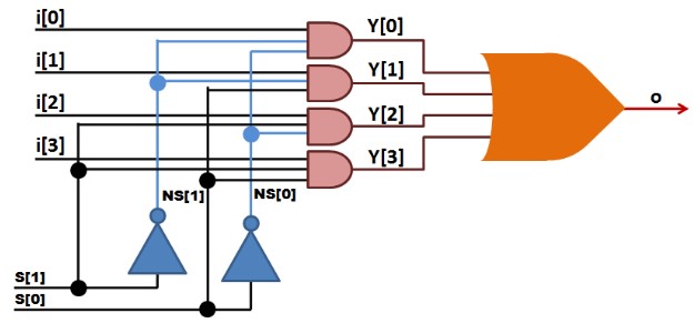
  module Mux_4_1_gate(input [3:0] i,input [1:0] s,output o);
  wire NS0, NS1;
  wire Y0, Y1, Y2, Y3;
  not N1(NS0, s[0]);
  not N2(NS1, s[1]);
  and A1(Y0, i[0], NS1, NS0);
  and A2(Y1, i[1], NS1, s[0]);
  and A3(Y2, i[2], s[1], NS0);
  and A4(Y3, i[3], s[1], s[0]);
  or O1(o, Y0, Y1, Y2, Y3);
  endmodule
Switch level is the lowest level of abstraction provided by Verilog. A module can be implemented in terms of transistors, switches, storage nodes, and the interconnections between them. In Verilog HDL transistors are known as Switches that can either conduct or open. Designing at this level requires knowledge of switch-level implementation details.