Advanced Physical Design using OpenLANE/Sky130 - Repository by Nuno Antunes (nuno.antunes@low-end.net)
hd high density fd foundry sc standard cell
ss slow slow ff fast fast tt typical typical
XXXC temp lvXX voltage
FF = Flip Flops/Lathes/rEGISTERS
A1, I1 = Standard Cells (AND/OR/NOT)
Dimensions are based on the standard cells/flip flops size.
Core, where logic is placed And Die, the semiconductor material where the core is fabricated.
- Utilization Factor = Area occupied by Netlist/Total area of the Core.
- Ideally 0.5/0.6 Utilization factor is used.
- Aspect Ratio = Height/Width
- Reusable combinational logic "Black Boxes" as IP's or modules.
- Only input/output are defined externally.
- Example: Memory, Clock gating cell, Comparator, Mux.
- Arrangement of Preplaced Cells/IP's in a chip is referred as Floorplanning
- Pre-defined locations, before automated placement-and-routing is performed
- Locations are dependent on design
During a logic state change an increased demand on current behavior happens. Resistance in a non-idea circuit means there are multiple voltage drops betwen the supply and logic circuit.
- Noise Margin : voltages should be inside a logic margin value (NM_l or NM_h) do be detected as 0 or 1, respectively. Voltage drops can affect the result for the logic outcome (undefined region). Decoupling capacitors are placed next to the preplaced cells to prevent the voltage drops during transition.
After local communication, power supply communication is required. For driver/load pairs, the communication link between two devices needs to be taken into account - this means a disturbance that results in a voltage/ground bounces.
This means that multiple Vdd/Vss pairs might be required to ensure adequate supply is delivered.
- This is often defined as the mesh, with Vdd and Vss on horizontal or vertical lines.
Taking into account the inputs, outputs and preplaced cells, the netlist is defined (via VHDL/Verilog).
Normally input and output pins are placed at opposite sides of the core.
Pin placement also depends on where the logic blocks are placed - this requires a full understanding of the design.
The communication ("handshake") between frontend team (that defined the network connectivity) and backend team (that defines the pin placement) is also critical.
Clock ports are bigger in size, as the clock drives the flip flops and require more current/less resistance.
The final step is blocking the areas for logical cells - Logical Cell Placement Blockage.
This ensures automatic placement and routing will not place cells in the blocked areas.
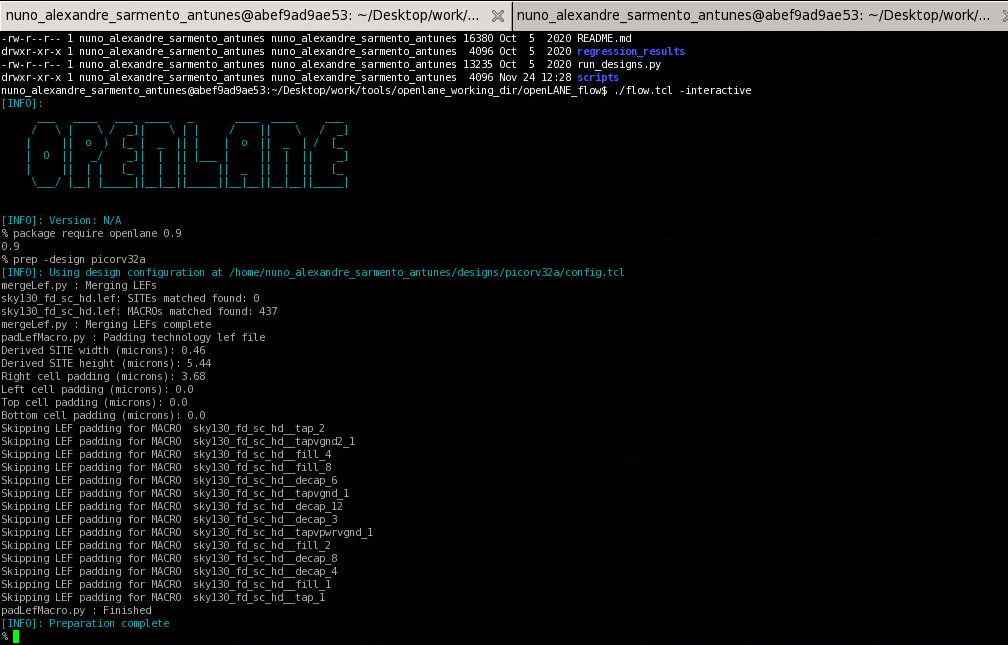
Required commands for openLAnE flow (interactive):
./flow.tcl -interactive
Inside flow, add the required package:
package require openlane 0.9
For preparation, it is possible to define a single "tag" that will be the folder used for the project run (without tag, folder name will be date/time based).
prep -design picorv32a -tag trial_run1
You can view configuration variables using the echo command.
echo $env(CLOCK_PERIOD) 15.000
In order to create further changes from the prep, add <code<-overwrite to the command.
prep -design picorv32a -tag trial_run1
This allows to apply any changes - everthing will be erased. An option to further change configuration during the run is using the set command:
set ::env(CLOCK_PERIOD) 15.000
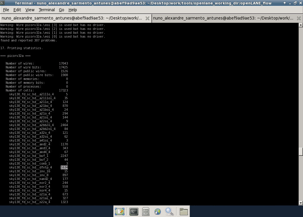
Finally, we can run the sythesis stage:
run_sythesis
Continuing from Day 1, sythesis was done. Next stage is floorplan.
Switches for configuration (including floorplan) can be found on $OPENFLOW/configuration/Readme.md:
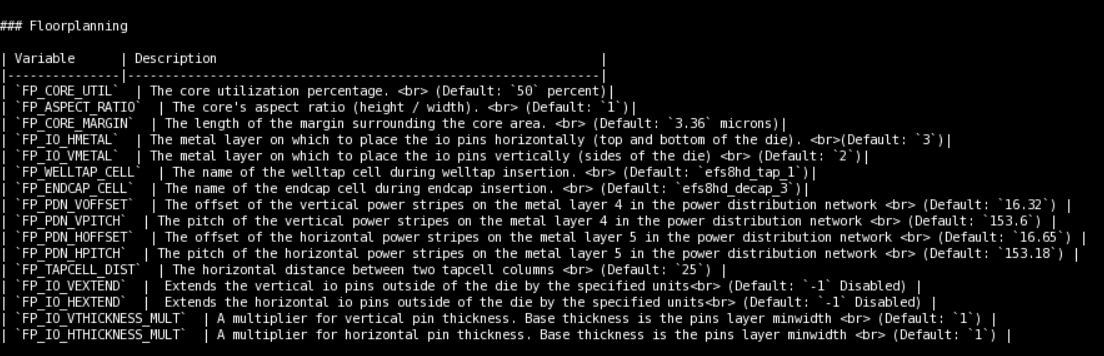
As you move into the flow, it might be useful to modify parameters as needed. For example, during the placement stage, PT_TARGET_DENSITY might be widely spread for condition analysis, and then set closer to dense to test timing constraints during design closure.
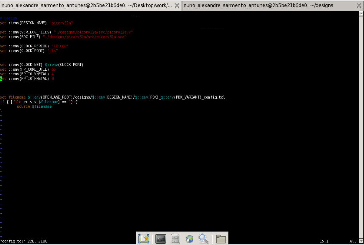
From a design folder, these parameters can also be applied to ./config.tcl, for example:
set ::env(FP_CORE_UTIL) 65
For now, we are adding some configuration values to the design - FP_CORE_UTIL to 65, FP_:
In OpenLANE flow interactive, assuming the synthesis was completed in the same way as day1, we can start the placement:
run_floorplan
TODO: UNITS DISTANCE MICRONS 1000 ; (0.001 mm) DIEAREA ( llx lly ) ( urx ury )
Rrom the result/floorplan foldder, it is possible to run magic to visually inspect the floorplan result:
magic -T ~/Desktop/work/tools/openlane_working_dir/pdks/sky130A/libs.tech/magic/sky130A.tech lef read ../../tmp/merged.lef def read picorv32a.floorplan.def &
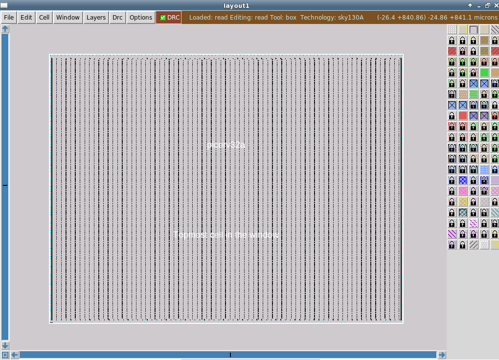
Libraries contain multiple variants of standard cells (logic gates, buffers, inverters, dff, latch, IGC) including:
- w/h of cell
- delay information of cell
- required conditions of cell (venn conditions)
- different threhold voltage (hVt, lVt) for the cell
- but also various shapes for same block
During the placement step in openLANE, the standard cells are placed in the die, attempting to preserve signal integrity based on the input/output pins, and adding buffers between elements if distance becomes an issue.
run_placement
This results in a legal placement
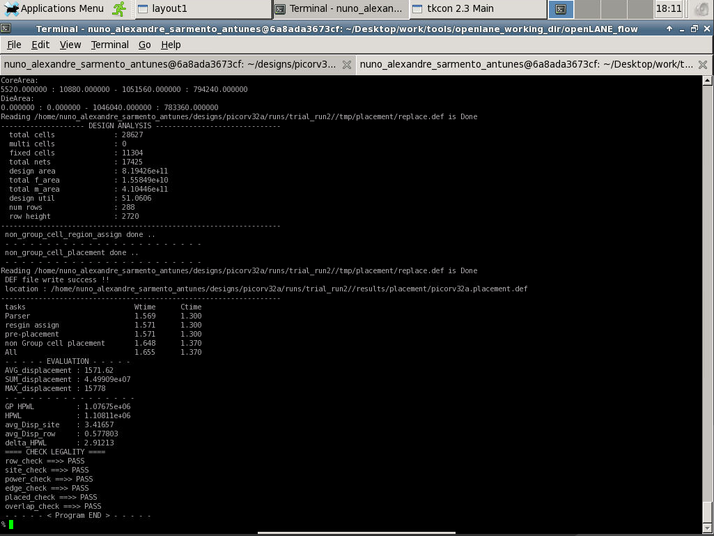
And it is also possible to use magic to view the cell placement.
magic -T ~/Desktop/work/tools/openlane_working_dir/pdks/sky130A/libs.tech/magic/sky130A.tech lef read ../../tmp/merged.lef def read picorv32a.placement.def &
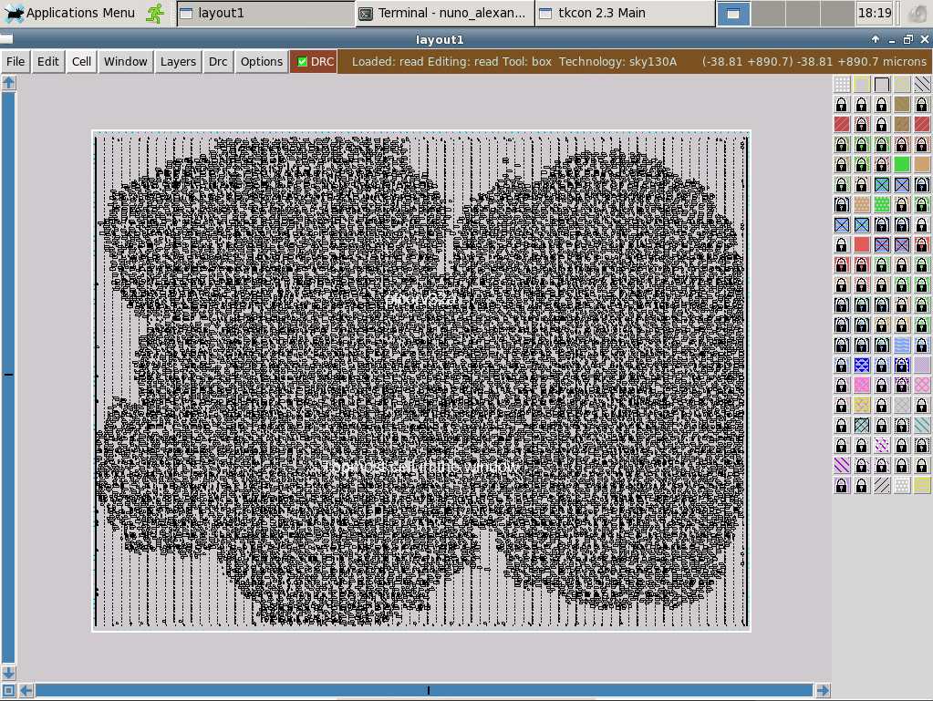
With the standard cells placed, we should look into the standard cell design itself.
In a library a standard cell is designed by using the several elements, that we divide in three sections:
- Inputs
- Process design kits (PDKs) : DRC&LVS rules, SPICE models, library and user-defined specs -> normally provided by foundry.
- Example DRV&LVS input parameters: poly width, extension over active, poly to active spacing
- Example Spice input parameters: values for dynamic behavior (Threshold voltage, linear region, saturation region equations)
- Example library and user-defined parameters: cell-height, supply voltage, pin location, drawn gate-length
- Process design kits (PDKs) : DRC&LVS rules, SPICE models, library and user-defined specs -> normally provided by foundry.
- Cell design
- Circuit design
- Taking into account the transistor requirements (eg. current and switching threshold) values determine requirements for the circuit.
- Layout design
- From the circuit design, extract paths for pmos and nmos networks
- Obtain Euler's path for both
- Draw stick diagram
- Convert into layout
- Characterization
- The step that helps getting timing, noise, power characteristics <- We will follow deeper into this.
- Circuit design
- Outputs
- CDL (Circuit Description Language)
- GDSII
- LEF
- Extracted spice netlist (.cir)
** Characterization flow
- Read Models (NMOS/PMOS) (and tech file)
- Read extracted Spice netlist
- Recognize behavior of the cell
- Read the subcircuits of the cell
- Attach the necessary power sources
- Apply the stimulus
- Provide the necessary output capacitance(s)
- Provide the necessary simulation commands
All of this information is fed to the characterization program GUNA, generating timing, noise and power .libs.
** Timing characterization
Timing threshold definitions:
slew_low_rise_thr- low V threshold for slew rise (typ 20% of waveform)slew_high_rise_thr- high V threshold for slew rise (typ 80% of waveform)slew_low_fall_thr- low V threshold for slew fall (typ 20% of waveform)slew_high_fall_thr- high V threshold for slew fall (typ 80% of waveform)in_rise_thr- input waveform rise delay (typ 50% of waveform)in_fall_thr- input waveform fall delay (typ 50% of waveform)out_rise_thr- output waveform rise delay (typ 50% of waveform)out_fall_thr- output waveform fall delay (typ 50% of waveform)
*** Delay calculations:
Buffer
time(out_rise_thr) - time(in_rise_thr)
Inverter
time(out_fall_thr) - time(in_rise_thr)
Choosing threshold point (ensuring in___xxx___thr is earlier than out___xxx_thr) is critical for characterization. This can be even more challenging if the circuit isn't optimized.
*** Transition time
time(slew_high_fall_thr) - time(slew_low_fall_thr)
time(slew_low_rise_thr) - time(slew_high_rise_thr)
*** Output current waveform
We will see this at a later stage.
We will be using a initial cell design from GitHub to save time for lab. Information about the standard cell used can be found at vsdstdcelldesign.
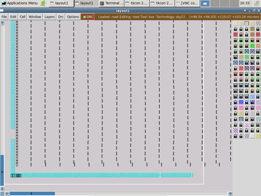
This is a quick test of the ability to change parameters during the openLANE flow. In this case an alternative floor IO placer (from 1 - random equidistant, to 2). From our loaded previous design, we perform:
set ::env(FP_IO_MODE) 2
And we then do run_floorplan again. The IO pin organization changes accordingly:
Here we quickly go over the netlist description of the inverter circuit as shown in a SPICE deck.
Component connectivity for this circuit:
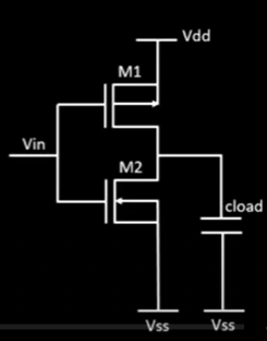
- Vin connects to M1 and M2 gate
- PMOS (M1) source connects to Vdd
- NMOS (M2) source connects to Vss
Component values:
- cload (load capacitor) is set to 10fF (we will see how to properly calculate this value later)
- PMOS W/L = 0.375u/0.25u
- NMOS W/L = 0.375u/0.25u
(ideally PMOS should be 2x, 3x wider)
Vin = 2.5V (related to channel site - 0.25 -> 2.5V) Vdd = 2.5V Vss -> common to supplies.
Nodes are identified in SPICE netlist and named:
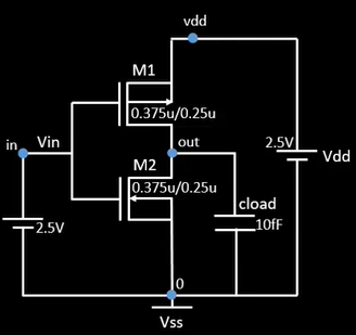
From here we can start describing the spice deck, starting with the MOSFET.
*** MODEL Description ***
*** NETLIST Description ***
M1 out in vdd vdd pmos W=0.375u L=0.25u
M2 out in 0 0 nmos W=0.375u L=0.25u
For a MOSFET, the description is
- For example : M1 has drain to "out" node, gate to "in" node and substrate and source nodes are connected to "vdd" node -
M1 out in vdd vdd pmos W=0.375u L=0.25u
For passive and voltage sources the format is :
- For the 10fF cload capacitor between node "out" and "0" -
cload out 0 10f - For the 2.5V voltage source Vdd between node "in" and "0" -
Vdd in 0 2.5
Adding the remaining components, simulation commands, and model library:
*** MODEL Description ***
*** NETLIST Description ***
M1 out in vdd vdd pmos W=0.375u L=0.25u
M2 out in 0 0 nmos W=0.375u L=0.25u

cload out 0 10f

Vdd vdd 0 2.5
Vin in 0 2.5
*** SIMULATION Commands ***
.op
.dc Vin 0 2.5 0.05
*** .include tsmc_025um_model.mod ***
.LIB "tsmc_025um_model.mod" CMOS_MODELS
.end
.dc Vin 0 2.5 0.05 - performs sweep of Vin from 0 to 2.5V at steps on 0.05.
With this deck we can test the model on SPICE for the static behavior - for example changing the W/L ratio for the PMOS transistor:
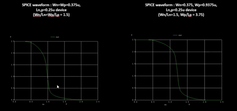
CMOS inverter robustness:
- Switching threshold (Vm) - point where Vin = Vout
- Vm should be far from the threshold conditions of the cell.
We can see how for the CMOS inverter Vm relates to the W/L ratio, so for the inverter, we can determine the expected Vm based on the W/L ratio of PMOS and NMOS MOSFETs.
For a dynamic simulation, we set Vin with a pulse signal, (2.5V, 10ps rise/fall, 1ns pulse length and 2ns period). Simulation is replaced with a transient analysis from 10ps to 4ns:
*** MODEL Description ***
*** NETLIST Description ***
M1 out in vdd vdd pmos W=0.375u L=0.25u
M2 out in 0 0 nmos W=0.375u L=0.25u

cload out 0 10f

Vdd vdd 0 2.5
Vin in 0 0 pulse 0 2.5 0 10p 10p 1n 2n
*** SIMULATION Commands ***
.op
.tran 10p 4n
*** .include tsmc_025um_model.mod ***
.LIB "tsmc_025um_model.mod" CMOS_MODELS
.end
This allows us to identify the rise and fall delay.
To clone the cell design from github we use on the ~/design folder:
git clone https://github.com/nickson-jose/vsdstdcelldesign.git
This creates the git structure in the folder vsdstdcelldesign
This cell already includes the inverter designs and we can perform Spice extractions and run simulations. We will first copy the magic tech file to this location:
cp ~/Desktop/work/tools/openlane_working_dir/pdks/sky130A/libs.tech/magic/sky130A.tech .
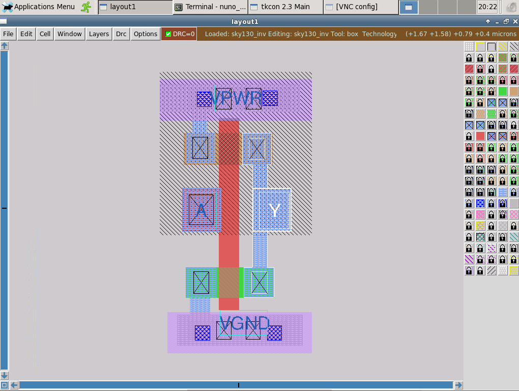
This allows us to view the sky130_inv.mag file as follows:
magic -T sky130A.tech sky130_inv.mag &
And we can then view the physical design of the inverter.
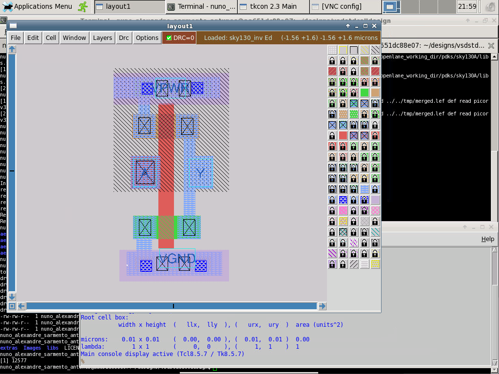
This is a basic introduction to CMOS fabritation, mostly meant to explain the several steps and mask requirements:
We require a silicon substrate (the wafer) to implement active regions.
- Selecting subtrate - P-Type, high resistivity (5~50 Ohms), doping level (10^15 cm^3), orientation (100). Doping is lower than 'well' doping used for active regions.
- Create active region for transistors:
- Create isolation between pockets using SiO2 (40nm), Si3N4 (80nm) layers over substrate.
- 1um photoresist is added
- Add Mask1 to protect from UV light. UV light will activate exposed areas and photoresist is removed after developing.
- Remove Mask1. The exposed areas can be individually manipulated.
- Etch off Si3N4 from exposed areas.
- Remove photoresist layer. This leaves photoresist areas with Si3N4.
- Areas with SiO2 exposed (the ones without Si3N4 layer) will grow after passing an oxidation furnace.
- The oxidized SiO2 now forms isolation islands for the transistors. This process is called LOCOS - Local Oxidation of Silicon.
- The areas where Si3N4 and the oxidized SiO2 meet are also called "Bird's beak"
- Finally strip out Si3N4 with hot phosphoric acid.
- Formation of N-well and P-well
- Add photo resist, and define Mask2 to protect one of the transistor regions.
- Expose to UV light, so it removes photoresist of unprotected area after develop.
- Remove mask and difuse Borom (P-type material) using ion implantation (high evergy, ~200keV). This creates a P-type layer "P-well".
- Perform steps 1-2 to the other transistor area. The implantation process uses phosphorus, this creates a N-type layer "N-well".
- Take the die into a high temperature furnace. The Drive-in diffusion will increase the size of both wells into the substrate.
- This design feature where both types of transistors are grown in known as a twin tub process.
- N-well will be used for a PMOS transistor, and P-well for a NMOS transistor.
- Formation of gate terminal
- Gate terminal defines threshold voltage, so the values defined here (NA - Doping concentration and Cox - Oxide capacitance) are important.
- Maintain doping concentration. Mask4 protects one of the transistors - in this case P-well is performed.
- A low energy Boron implant that applies a doping concentration on the P-well. a "P" layer is set. Note that the SiO2 is still getting damaged.
- "N" layer is set with Mask5 and a low energy Arsenic doping. Notice that both these steps set the doping concentration for the transistors.
- Remove damaged SiO2 with etched hydrofluoric(HF) acid. Then regrow SiO2 again to get a high quality oxide (~10nm thin). This step sets the Oxide capacitance.
- Deposit a thick (0.4um) polysilicon layer, and lower the gate resistance with N-Type ion implants.
- Create a Mask6 for the gate areas, allowing to etch out the polysilicon outside of the gate areas. This completes the gate with full control of parameters.
- Lightly doped drain (LDD) formation
- We need to implement P+, P-, N doping profiles to set the PMOS drain, and N+, N-, and P doping profiles for the NMOS drain.
- Mask7 is set protecting PMOS area. P-well is unprotected and we do N-type lightly doped implementation (N-) implant around the gate.
- Mask8 is set protecting NMOS area. N-well is lightly P-type doped to set the (P-) implant around the gate.
- Side-wall spacers are added around the gate by adding a thick (0.1um) So3N4 or Sio2 layer and performing plasma ansiotropic etching.
- Side-wall spacers help keep N- and P- implants during the next steps of doping to form the source and drain.
- Source - drain formation
- A thin screen oxide is added to avoid heavy channeling into the substrate during implants.
- Mask9 is set over the PMOS area. NMOS area is strongly implanted with Arsenic, with the N+ implant taking over most (but not all) of the N- area and some P-well.
- Mask10 is set over the PMOS area. PMOS area is strongly implanted with Boron, with the P+ implant taking over most (but not all) of the P- area and some N-well.
- We expose the half built MOSFETs to high temperature anelling, forcing P+ and N+ impurities further into the P-wells and N-wells.
- Local interconnect formation
- Remove the thin screen oxide with HF solution from the previous step, making gate, source and gate open.
- Deposit titanium on wafer surface, using sputtering. The whole structure is covered.
- Create the contact surface by heating the wafer in a N2 ambient for 60 sec, creating low resistant TiSi in areas that connect with the gate silicon.
- TiN is also produced over all the structure, that can be used for local communication.
- Mask11 is used to block the areas that should be local interconnects and RCA cleaning is used to etch off the unneeded TiN.
- Higher level metal formation
- The surface is now non linear - surface consists of many diferent levels of layers.
- Deposit a thick (1um) SiO2 layer doped with phosphorus or boron on wafer surface.
- Chemical mechanical polishing (CMP) is used to planarize the wafer surface.
- We use Mask12 to etch off the SiO2 where we want to "drill" the contact holes
- Deposit a thin layer (10nm) of TiN.
- Deposit a blanket tungsten layer (W) and perform CMP again
- Deposit an Aluminium layer
- Use Mask13 to etch out the aluminium to establish the contacts.
- The tugsten layer is defined as Metal0 layer, the first aluminium layer as Metal1 layer
- For firther layers we add another SiO layer and CMD
- Mask14 is used to drill contact holes, TiN is deposited, W fills the contacts, another aluminium layer is added.
- Mask15 used to drill the aluminium layer.
- The last level uses a strong dielectric (Si3N4), Mask16 is used to drill the contact points.
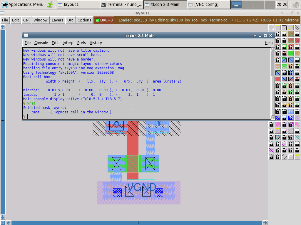
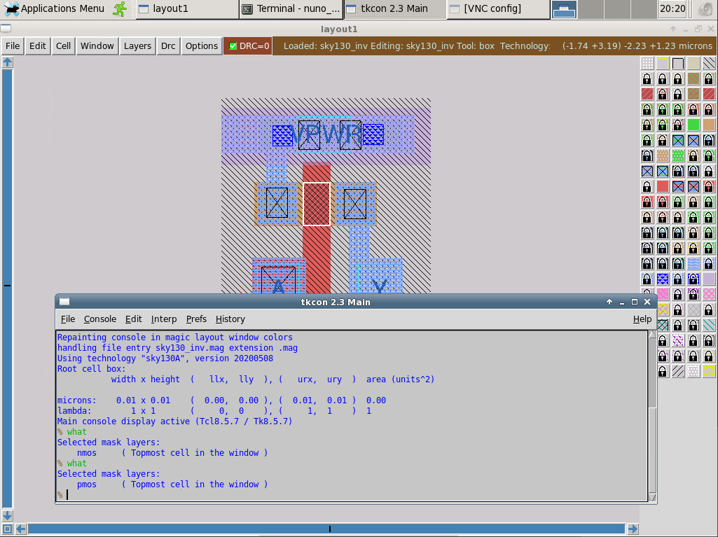
Going back to magic, we can quickly check the diferent layers used in CMOS. As before, hovering and pressing s allows to select a specific layer and typing "what" on the tcl window lets us se the named layer. For example the two pictures show that by selecting the polysilicon gate element we can see the nmos and pmos layers.
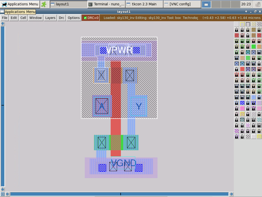
Pressing two times 's' lets us select the connected elements of a junction. For example here we can see the source connecting to VGND and VPWR respectively.
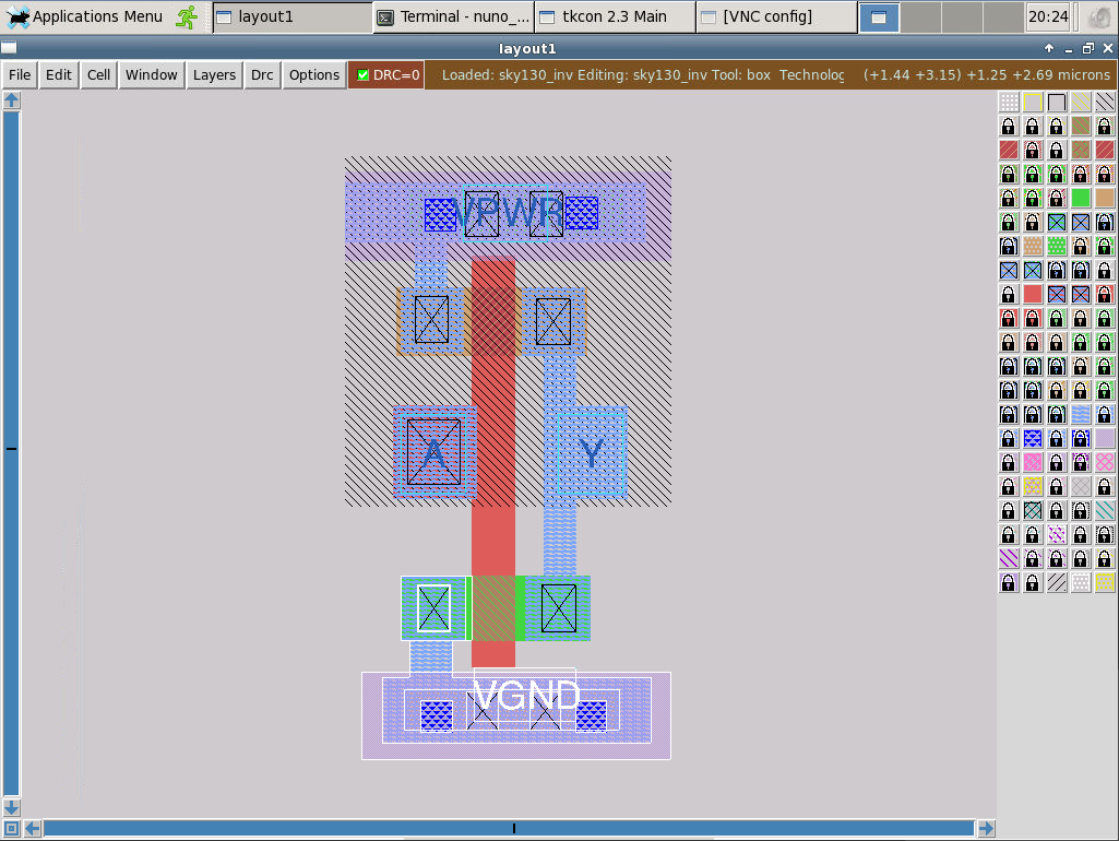
Likewise, the drain on both MOSFETs is connected to output pin Y
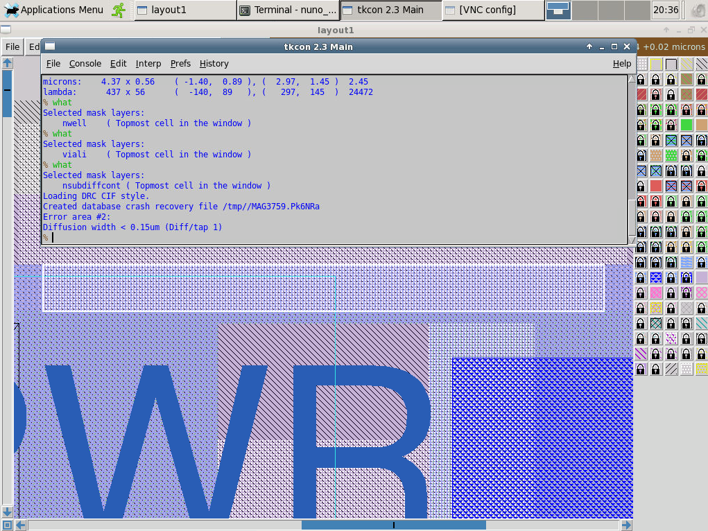
DRC (Design rule check) can also be performed. The DRC indicator will show any existing non-compliance and using menu option DRC->Show Next Error highlights the discrepancy as well as output the error on the tcl window:
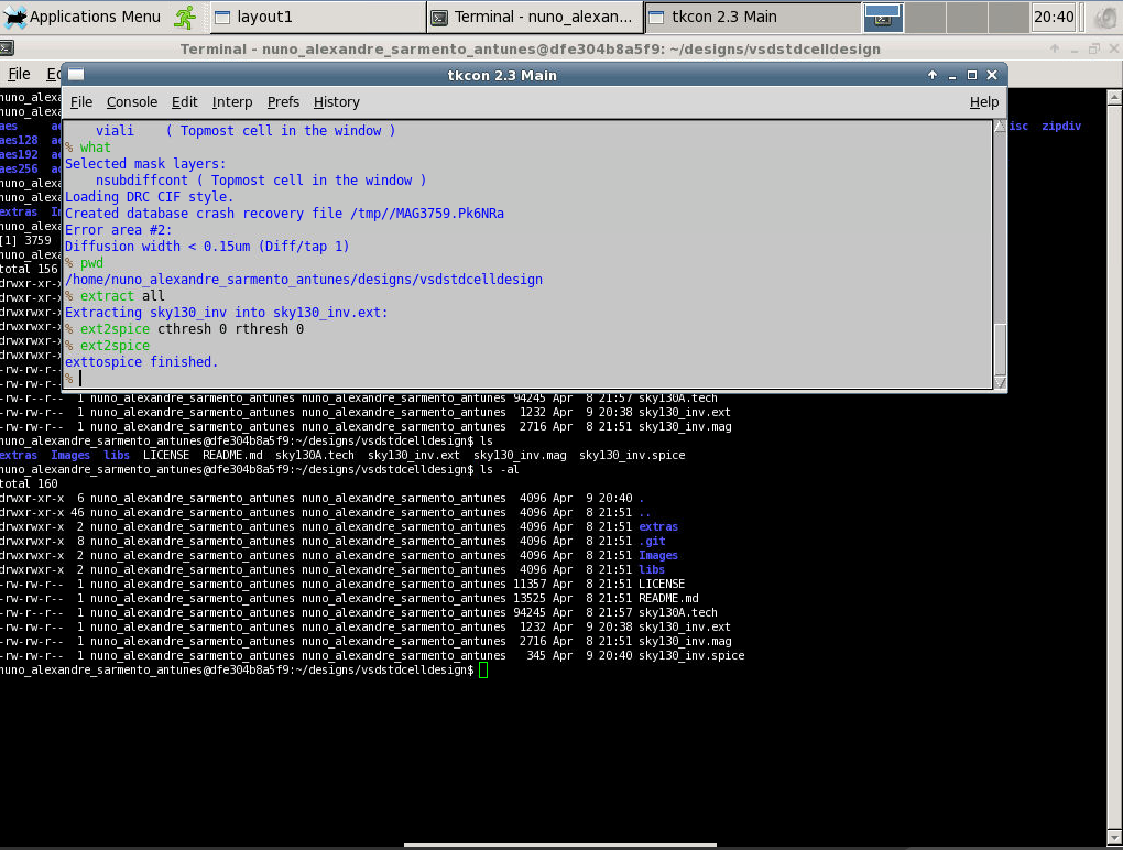
With a design open in magic we can export the related spice file. By default this will be done in the directory magic was started with (type pwd in tcl command window to verify). the sequence of commands to obtain the extracted SPICE deck is as follows:
extract all - this results in a .ext file being created
ext2spice ctresh 0 rtresh 0- set the parasitic capacitance and resistance threshold to 0 so all are present in the model
ext2spice - extract the file.
This results in the spice file (in this case sky130_inv.spice) being saved in the directory.
And we can verify the extraction.
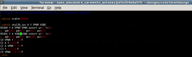
The extracted spice file needs some updates in onder to be usable:
- Scaling to be set to 0.01u (magic smallestunit)
- The related library for the mosfet models needs to be added (
.includecommands) - VDD (power) and Va supplies need to be added to the simulation.
- Accordingly, we need to add a VSS node at 0V to ground the power supplies and the inverter model.
- Finally we add the transient simulation command (
.tran), run and end the simulation.
The end result is as follows:
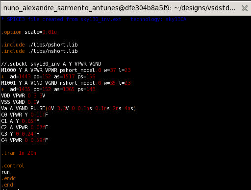
With the modified model, we can start ngspice from the terminal:
ngspice sky130a_inv.spice
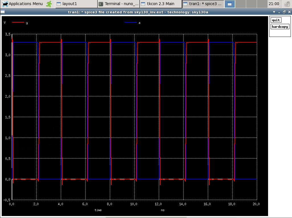
On a successfull load we can use the SPICE terminal to plot the output (y) over time and input (a):
'plot y vs time a'
We initially obtaint this image, that has a overshoot
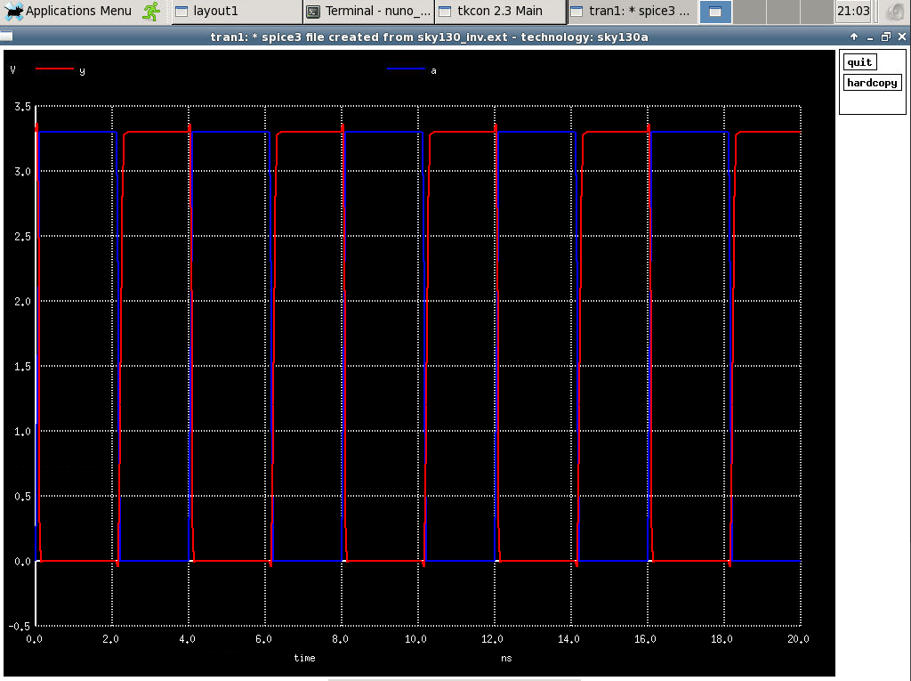
Going back to Spice and increasing the value of the load capacitance to 2fF
Characterizing the transient response
As discussed before in the spice simulation , we can extract the values by checking rise and fall times:
- Rise transition (20% to 80%)
- Fall transition (80% to 20%)
Propagation delay
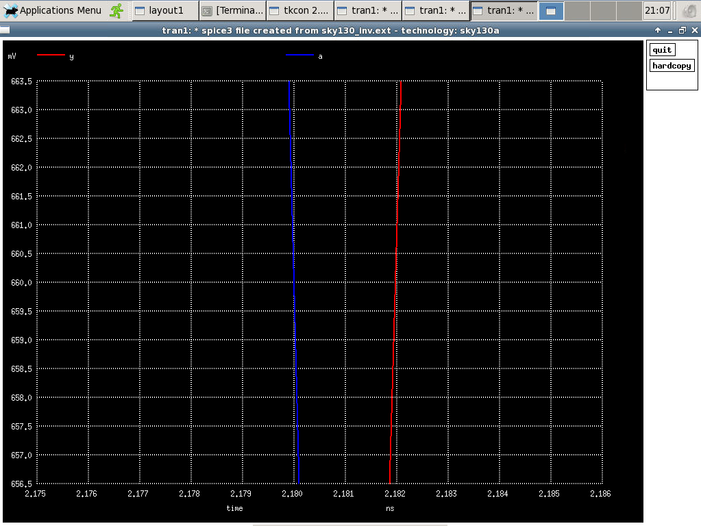

Extracking the values:
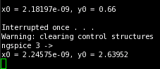
2.24575e-9 - 2.18197e-9 = 0.06378e-9 -> Rise time 0.064ns
Transition time
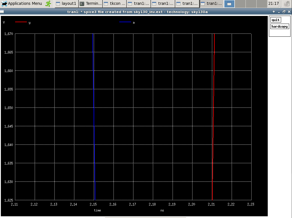
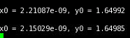
2,21087e-9 - 2,15029e-9 = 0.06058e-9 ns -> Propagation rise delay 0.06ns
This are the results given for a single temperature profile - TEMP = 27 and TNOM = 27
Here we will look into magic's DRC format, that is slightly different of other industry options. A lot of information about magic can be found at http://opencircuitdesign.com/magic - in particular the Using Magic and Technology Files sections are relevant for this lab.
- Technology files are important as they include a lot of information, more than normally found in other tools:
- Layer types, colors and patterns
- Electrical connectivity
- DRC rules
- GDS generation rules
- Device extraction rules to generate netlists
- Rules for interactive wiring
- etc...
The other important links for this section is the Google Skywater PDK (https://github.com/google/skywater-pdk) and related documentation (https://skywater-pdk.readthedocs.io/en/latest/)
You won't see implant layers in the magic layout view (they are generated on the output file).
The only way to see those layers is to use the cifsee command to highlight the areas where that layer will be generated on output.
http://opencircuitdesign.com/open_pdks/archive/drc_tests.tgz contains a series of files that we can use to test different DRC errors, as well as the technology file and a .magicrc startup script.
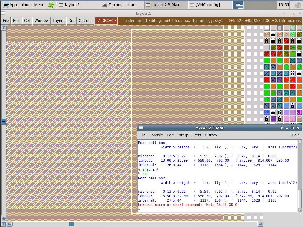
Let's open an example file (met3.mag) in magic
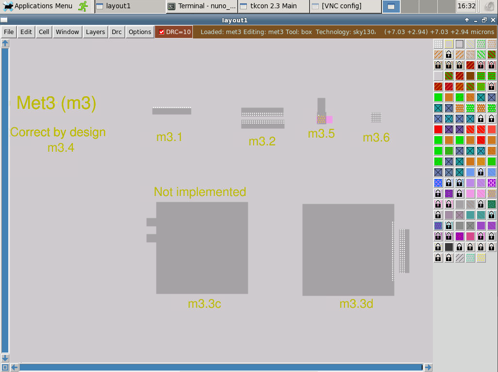
The white patches represent the DRC errors.
We can see the DRV errors by selecting the item and using the drc why command.
To see the automatic generation of via2 (automatically complying the m3.4 rule) we can create a box of m3contact and then using cif see VIA2 to display the mask layer for via2 generated on the GDS output. the cifoutput section of the tech file explain how to draw contact cuts. To clear this display (called feedback view) you can use feedback clear or feedclear
In order to verify deisgn rule m3.4 (Via2 must be enclosed by Met3 by at least 0.065 µm) we can measure the distance between a via2 and the cornet of the m3contact. We draw a box between the two sections and verify the width (0.13µm in this case) that is clearly larger than the DRC.
We now move to example poly.mag, with several rule examples that are not correctly parse. Here is an example of poly.9: Poly resistor spacing to poly or spacing (no overlap) to diff/tap 0.480µm
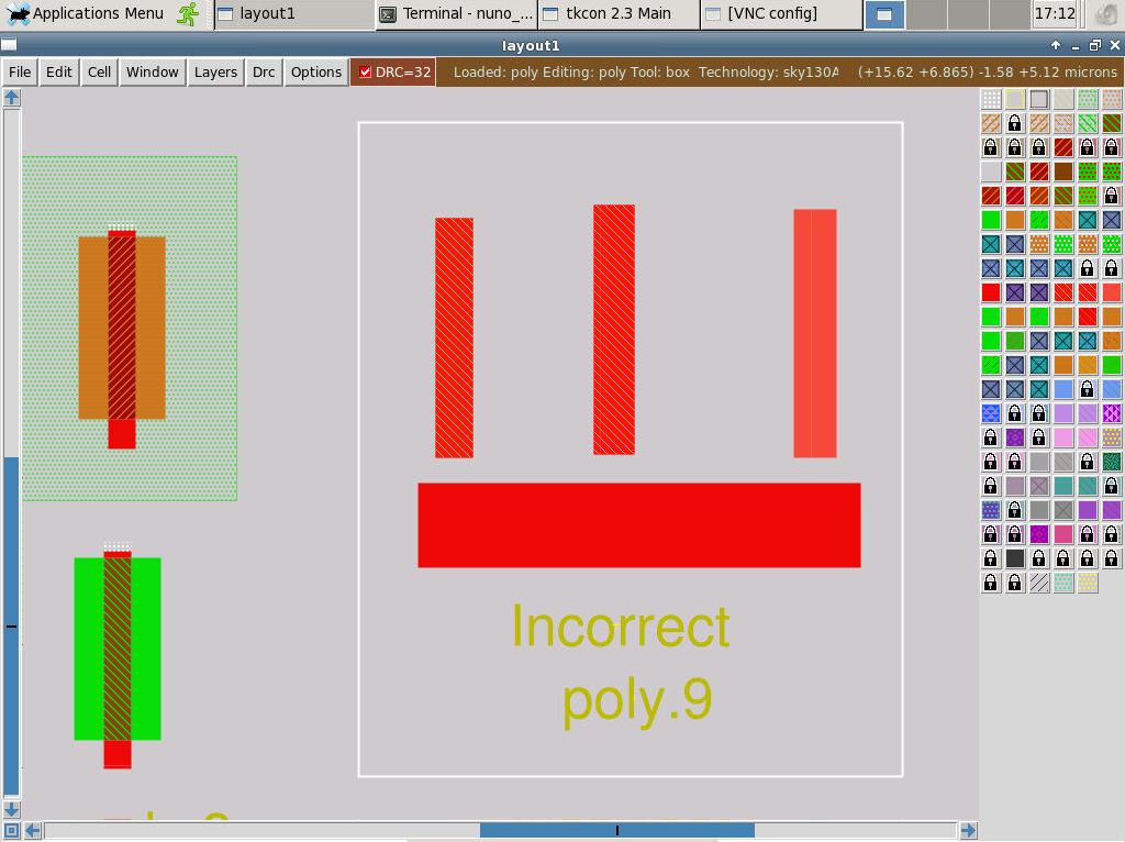
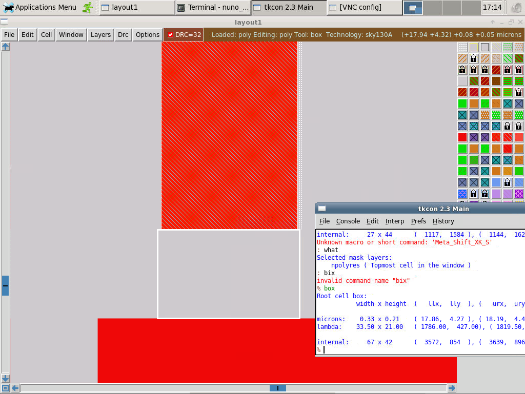
The separation between poly (visible on bottom) and npolyres (visible on top) is only 0.21µm, but no DRC is shown:
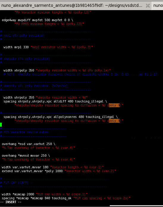
We can check the supplied sky130A.tech file and see the rule for poly.9 - and no attempt has been made to define the difference between poly resistor and poly (only to uhrpoly and xhrpoly). So we perform this by adding the new rules for alias allpolynonres - a short name for all non-resistive poly materials.
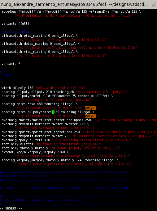
To update an open magic window with the tech file we can use tech load sky130A.tech on the tcl command line, followed by 'drc check'. The poly now show the DRC noncompliance expected by the rules:
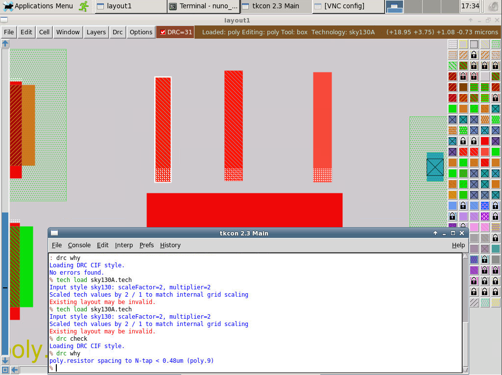
However, the example does not show spacing for dif or tap. We can generate examples for those:
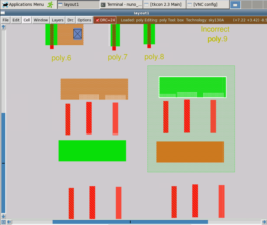
Is now visible that the DRC is not applying to the respoly layer - only the xhr and uhr poly have the full ruleset. However, that rule is already implemented for respoly and npolyres.
We return to the tech file to check that rules and extend it to the all diffres materials.
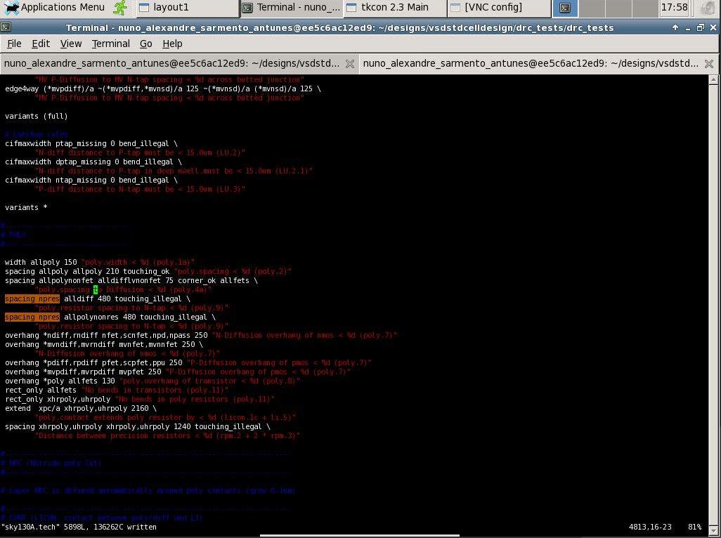
DRC is now visible for the diff material.
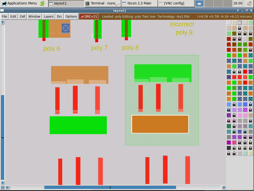
Now we move to a more challenging DRC problem. We will need to use the cifoutput operators to generate a complex geometric feature that features the DRC error.
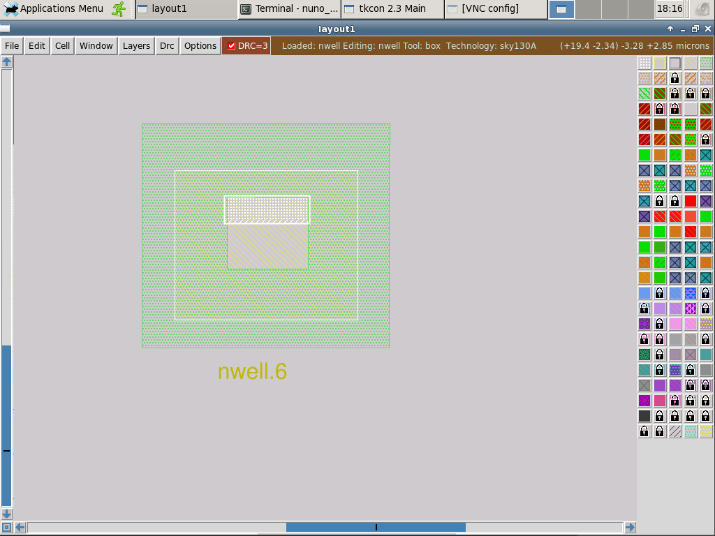
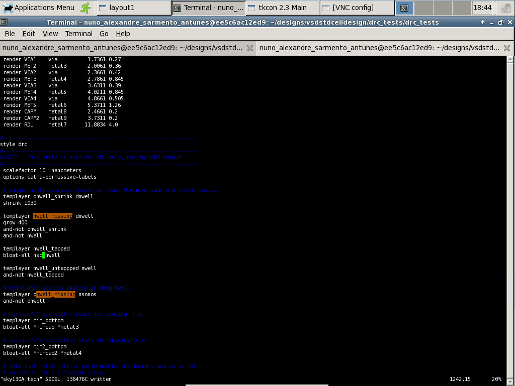
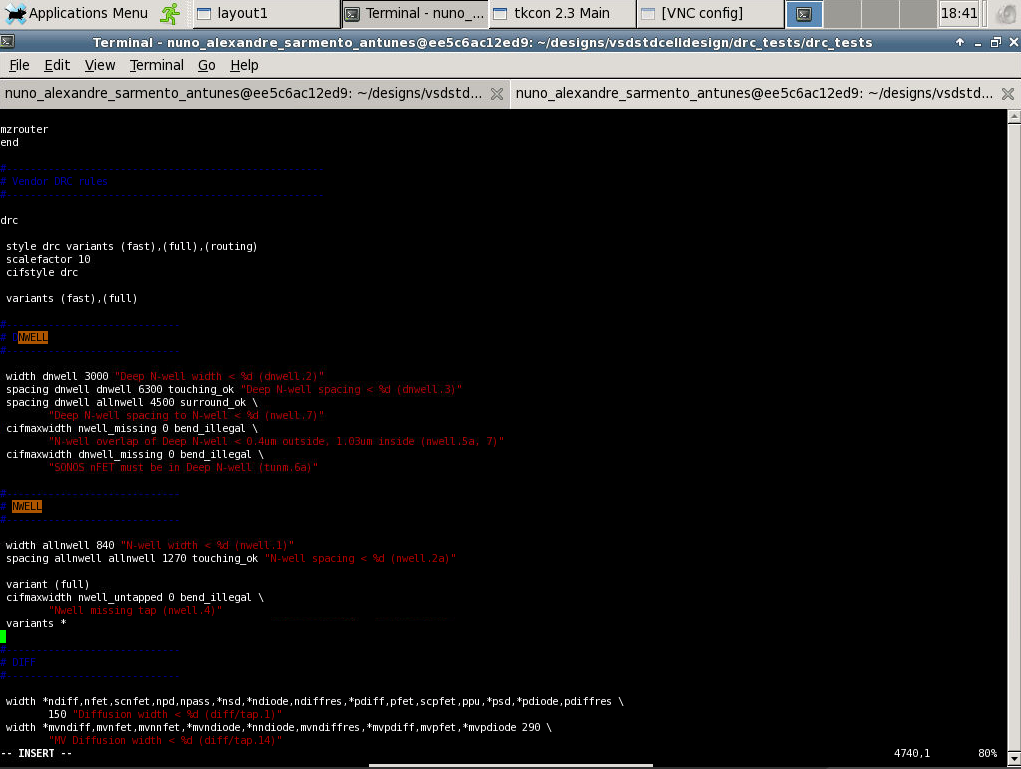
nwell.4 (All n-wells will contain metal-contacted tap (rule checks only for licon on tap)) is a rule that is not correctly implemented as seen on the nwell.mag file.
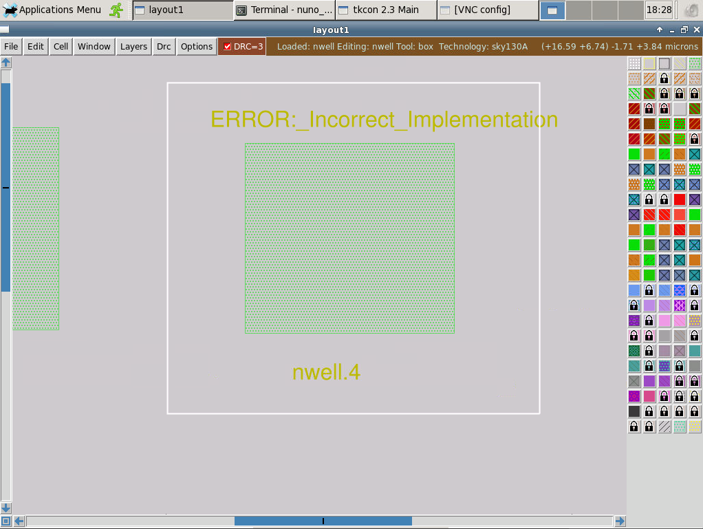
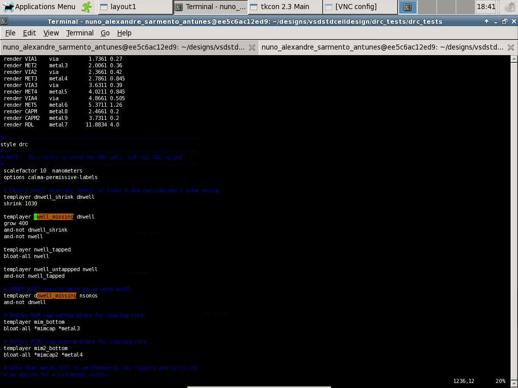
This n-well does not contain a mtap layer contact (named nsubstratencontact, or NSC) but no drc is generated. As there are no mtap element to measure, we can use the cifoutput operations to create this drc rule. Of particular use is the bloat-all operator and the binary operations.
Let's extract lef life from our inverter.
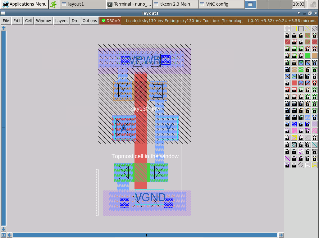
- Ensuring the grid can reach A and Y
- Width of standard cell LEF should be a xpitch multiple
- Height of standard cell LEF should be a ypitch multiple! image
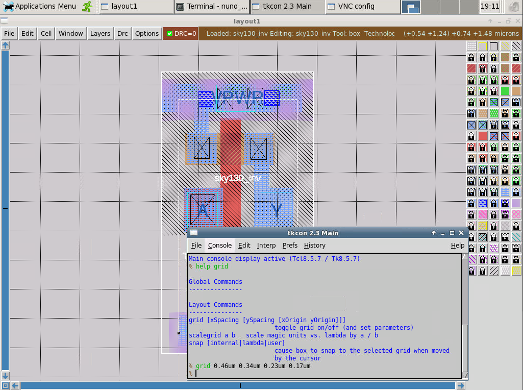
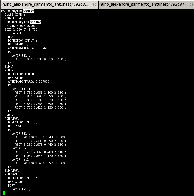
When extracting a LEF file, ports are extracted. This is how ports are defined (see nickson-jose github)
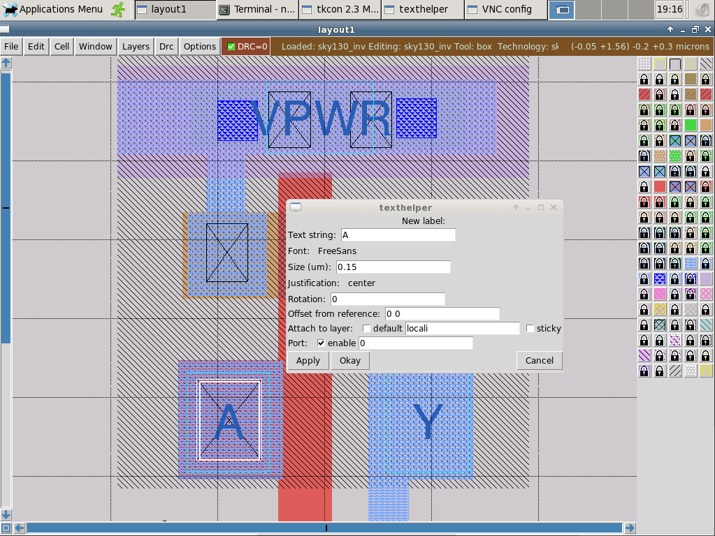
The LEF file creation is just a matter of using command lef write on magic's tcl terminal. This creates a file with the same name as the magic source file, but extension .lef (in this case sky130_vsdinv.lef).
- copy LEF file into src folder of picorv32a
- we also need a library to include the LEF element - we copy the openlane pdk libraries to the src foler as well

Add the rule to include the extra LEF files into picorv32a config.tcl
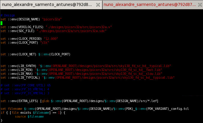
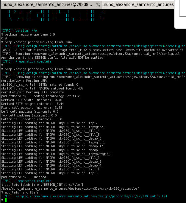
Then add the following commands before synthesis:
set lefs [glob $::env(DESIGN_DIR)/src/*.lef] add_lefs -src $lefs
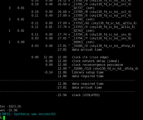
Synthesis fails with violated slack:
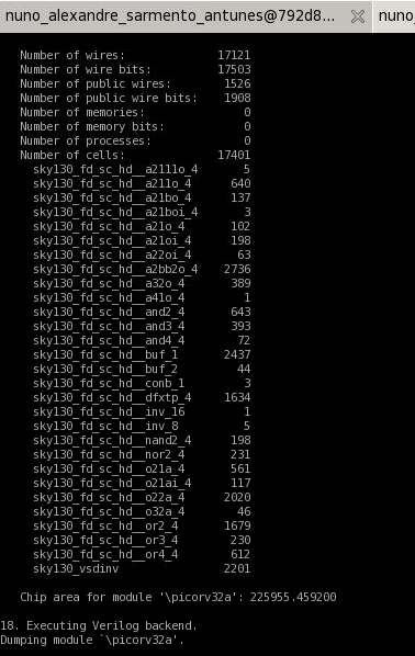
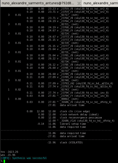
| SYNTH_STRATEGY | Strategies for abc logic synthesis and technology mapping
Possible values are 0, 1 (delay), 2, and 3 (area)
(Default: 2)|
| SYNTH_BUFFERING | Enables abc cell buffering
Enabled = 1, Disabled = 0
(Default: 1)|
| SYNTH_SIZING | Enables abc cell sizing (instead of buffering)
Enabled = 1, Disabled = 0
(Default: 0)|
with SYNTH_STRATEGY 2 / SYNTH_BUFFERING 0 / SYNTH_SIZING 1 Chip area for module '\picorv32a': 225955.459200 tns -1623.26 wns -15.96
with SYNTH_STRATEGY 1 / SYNTH_BUFFERING 1 / SYNTH_SIZING 1 Chip area for module '\picorv32a': 317725.974400 tns -88.54 wns -3.36
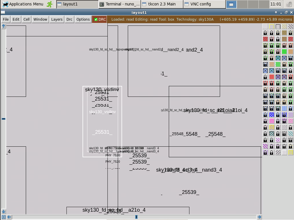
After run_floorplan and run_placement
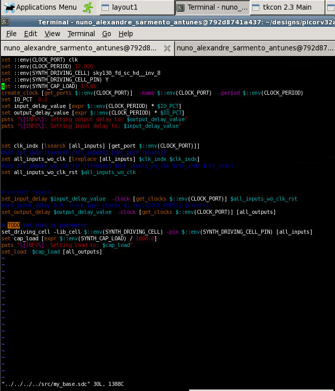
Preparing for OpenSTA
Kunal Ghosh - Co-founder (VSD Corp. Pvt. Ltd)
Nickson Jose - VSD VLSI Engineer