Architecture_details
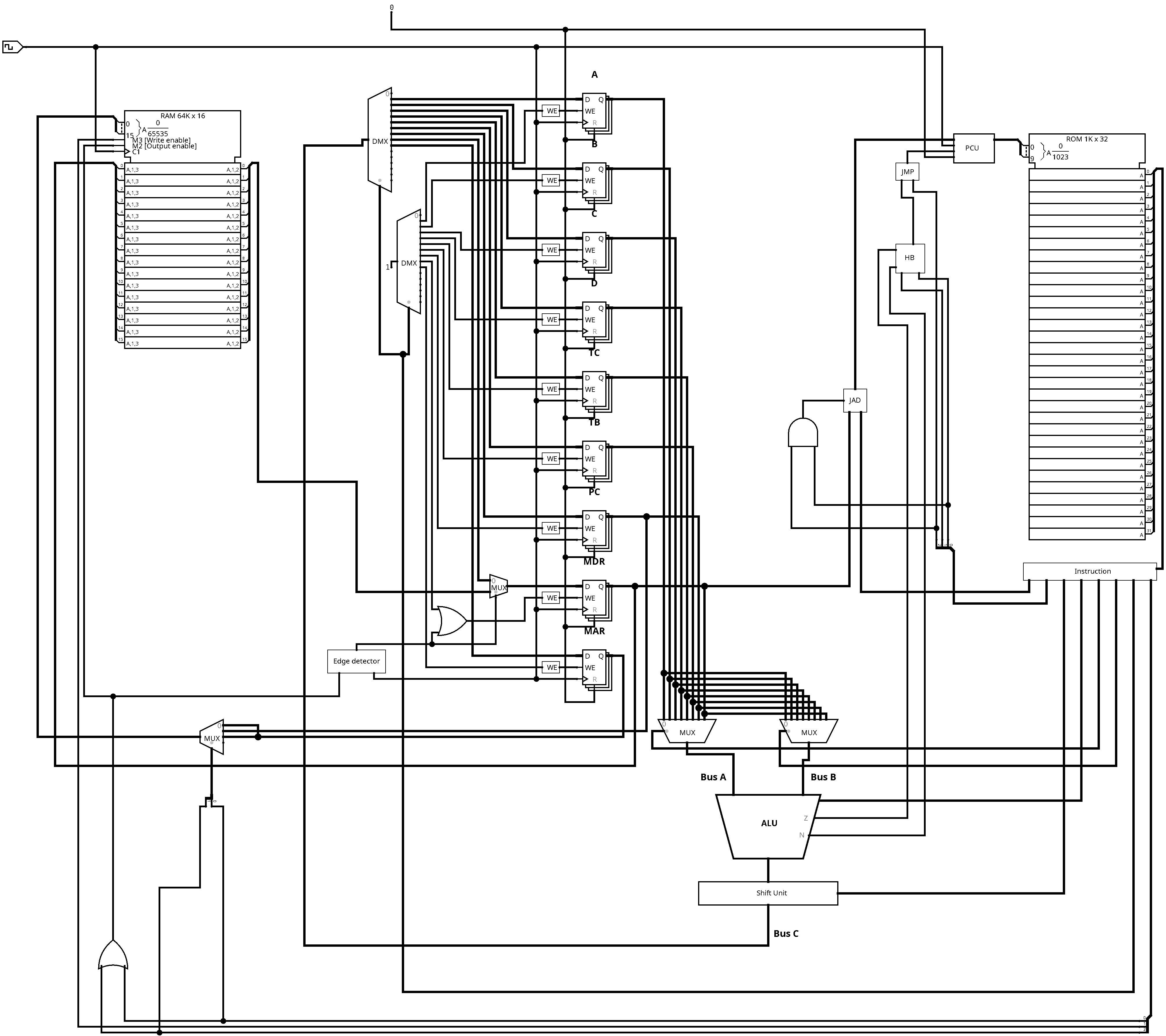
This page contains all the details about the architecture and how it works.
- A: General purpose register A
- B: General purpose register B
- C: General purpose register C
- D: General purpose register D
- TC (T)ape (C)ursor: Contains the cursor position
- TB (T)ape (B)ase: Used to contain base position of the tape
- PC (P)rogram (C)ounter: Contains the index of the current instruction
- MDR (M)emory (D)ata (R)egister: Contains the content of address in MAR
- MAR (M)emory (A)ddress (R)egister: Points to an address in RAM
All the registers are 16-bit. Every register apart from the last three can be used arbitrarily when it comes to writing micro-code programs.
MAR is the only register whose value can't be modified based on its current value, therefore its value can only be assigned to one of the other registers.
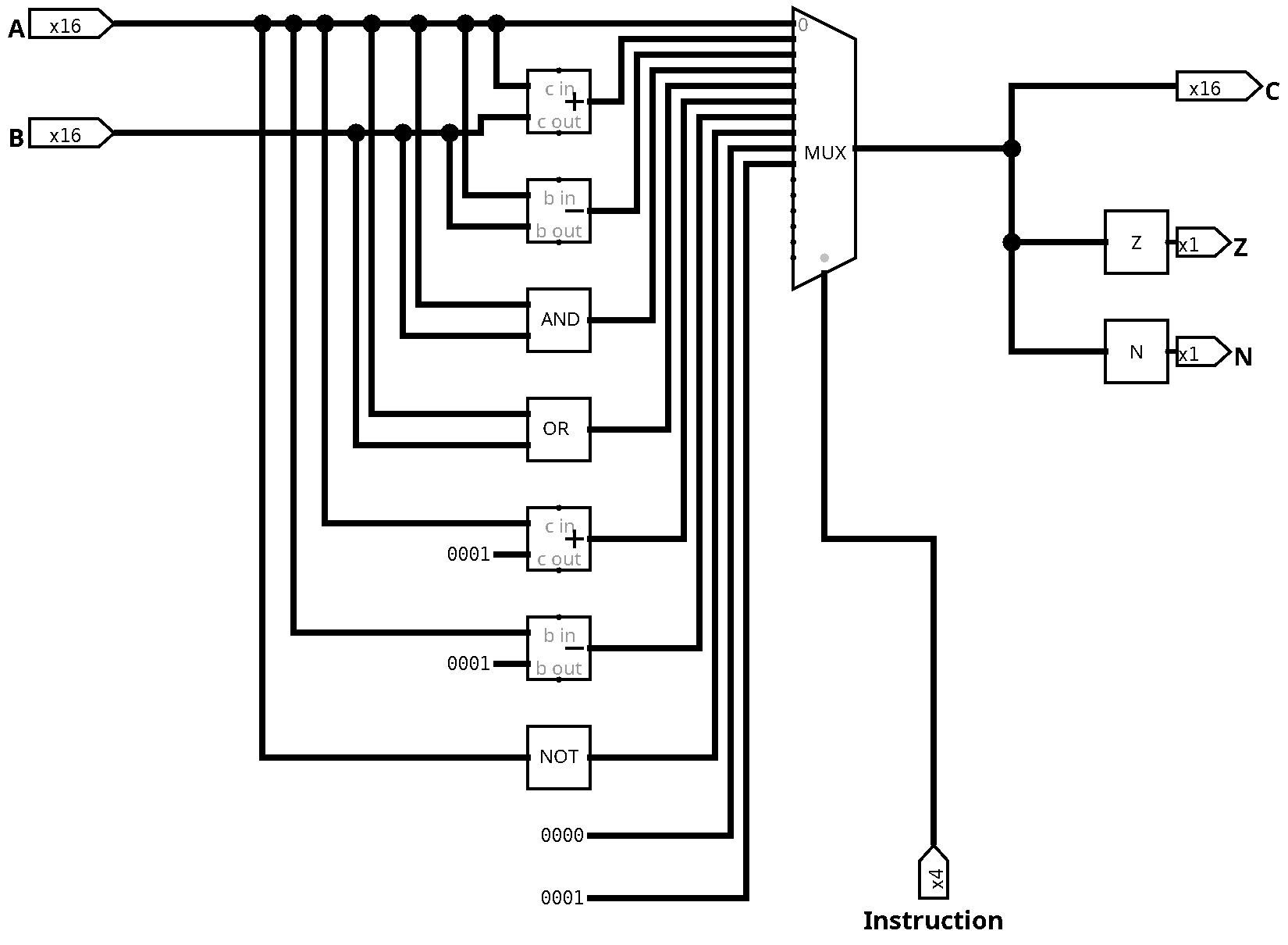
Here are all the ALU operations with their binary code:
- a: 0000
- a + b: 0001
- a - b: 0010
- a and b: 0011
- a or b: 0100
- a + 1: 0101
- a - 1: 0110
- not a: 0111
- 0: 1000
- 1: 1001
- -a: 1010
The Z flag is set to 1 when the ALU result is equal to zero, while the N flag is set to 1 when the ALU result is negative (the most significant bit is one).
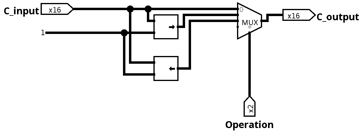
The shift unit can modify the ALU output and alter its value on the C bus. The shift unit takes as input the ALU result (C_input) and two bits that represent the operation.
- No shift: 00
- Left shift: 10
- Right shift: 01
Each shift is done only by one position. This operation doesn't affect the jump.
The A and B buses carry the two ALU inputs and they are selected with the help of two multiplexers (MUX).
You can address the registers on the A and B bus with the same values:
- A: 000
- B: 001
- C: 010
- D: 011
- TC: 100
- TB: 101
- PC: 110
- MDR: 111
The value on the C bus can serve as input to all of the 9 registers. This is done with the help of two multiplexers and the WE (Write Enable) circuit.
The first multiplexer is used to address the destination register while the second is used to target the WE circuit to write that data to the register. This second multiplexer simply sends a one to the WE.
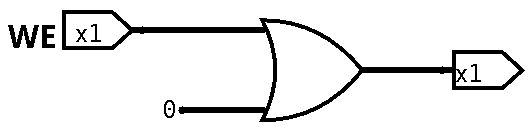
The WE circuit simply acts as an AND between zero and the second multiplexer output.
An important note is the fact that the C bus value can also not be stored in any register. This is useful to perform jumps on certain operations without having to store the result inside a used register.
The registers are addressed in this way:
- noreg: 0000
- A: 0001
- B: 0010
- C: 0011
- D: 0100
- TC: 0101
- TB: 0110
- PC: 0111
- MDR: 1000
- MAR: 1001
The jumps are performed by the circuit to the left of the ROM. The instruction circuit simply divides the ROM instruction into the various arguments.
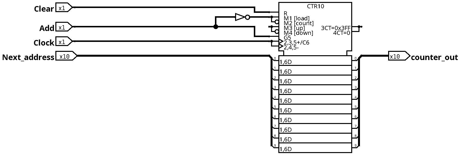
The PCU consists mainly of the Logisim Evolution counter and some of its inputs. The clear input is always set to zero by the external constant; Add instead is set to zero only when the CPU has to perform a conditional or unconditional jump. When the Add flag is set to zero, the load is automatically set to one so the CPU jumps to the given address. This address is contained inside the Next_address argument.
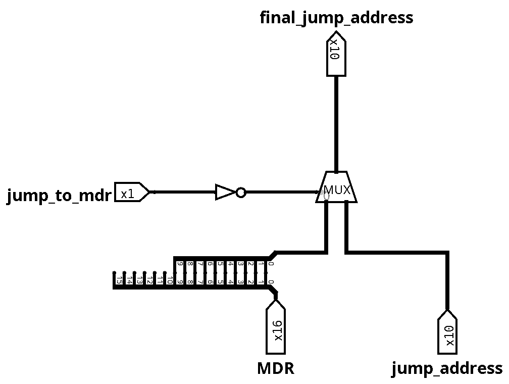
The JAD circuit consists simply of a multiplexer that regulates jumps to the first 10 bits specified inside MDR when necessary, else it jumps to the specified address (the next address).
The flag that allows jumping to the MDR content is set by the AND gate next to the JAD circuit that intercepts the jump to MDR instruction.
JAD substantially changes the normal jump address or replaces it with the first ten bits of MDR.
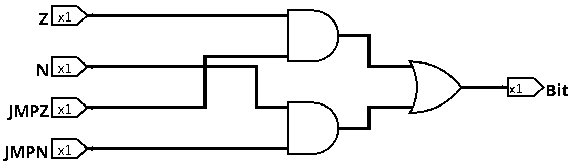
The output flag is set to one based on this condition:
(Z == 1 and JMPZ == 1) or (N == 1 and JMPN == 1).
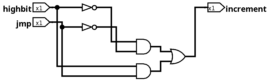
- No jump: 000
- Unconditional jump: 100
- Jump if zero: 010
- Jump if negative: 001
- Jump to MDR: 101
This processor performs memory operations with the help of the Edge detector, the OR gate, and the multiplexer located at the bottom left of the circuit.

The memory is read at the address contained inside MAR and its result is stored inside MDR. If the performed operation is to fetch data, the CPU reads the value of the cell whose address is equal to the PC register value.
- No operation: 000
- Reading: 100
- Writing: 010
- Fetching: 001
The edge detector is necessary because the memory needs roughly one clock cycle to perform every operation.
Each instruction consists of a 32-bit number. An instruction is structured in this way:
0000000000 000 00 0000 000 000 0000 000
Jump addr  JMP LR ALU  A   B   C    rwf
               SS
               11
- 10 bits: Jump address
- 3 bits: Jump operation (JMP)
- 2 bits: Shift (LS1 and RS1)
- 4 bits: ALU operation
- 3 bits: A bus (A)
- 3 bits: B bus (B)
- 4 bits: C bus (C)
- 3 bits: Memory operation (rwf)
- JMPU: 100
- JMPZ: 010
- JMPN: 001
- JMPMDR: 101
- No jump: 000
If the condition is correct, the computer jumps to the given address in ROM.
- LS1: 10
- RS1: 01
- No shift: 00
- a: 0000
- a + b: 0001
- a - b: 0010
- a and b: 0011
- a or b: 0100
- a + 1: 0101
- a - 1: 0110
- not a: 0111
- 0: 1000
- 1: 1001
- -a: 1010
- A: 000
- B: 001
- C: 010
- D: 011
- TC: 100
- TB: 101
- PC: 110
- MDR: 111
- A: 000
- B: 001
- C: 010
- D: 011
- TC: 100
- TB: 101
- PC: 110
- MDR: 111
- NOP: 0000 (Used to implement the NOP function)
- A: 0001
- B: 0010
- C: 0011
- D: 0100
- TC: 0101
- TB: 0110
- PC: 0111
- MDR: 1000
- MAR: 1001
- Reading: 100
- Writing: 010
- Fetching: 001
- No operation: 000