Repository navigation
Examples
Generator/Input/ holds three example boards. Each is a whole design, not a test of one feature:
a stack-up set in Board Setup, footprints, filled zones, silkscreen on both sides and a solder
mask colour of its own, saved by KiCad 7. Between them they use most of what KESE reads.
python run_KESE.py with no arguments exports all three.
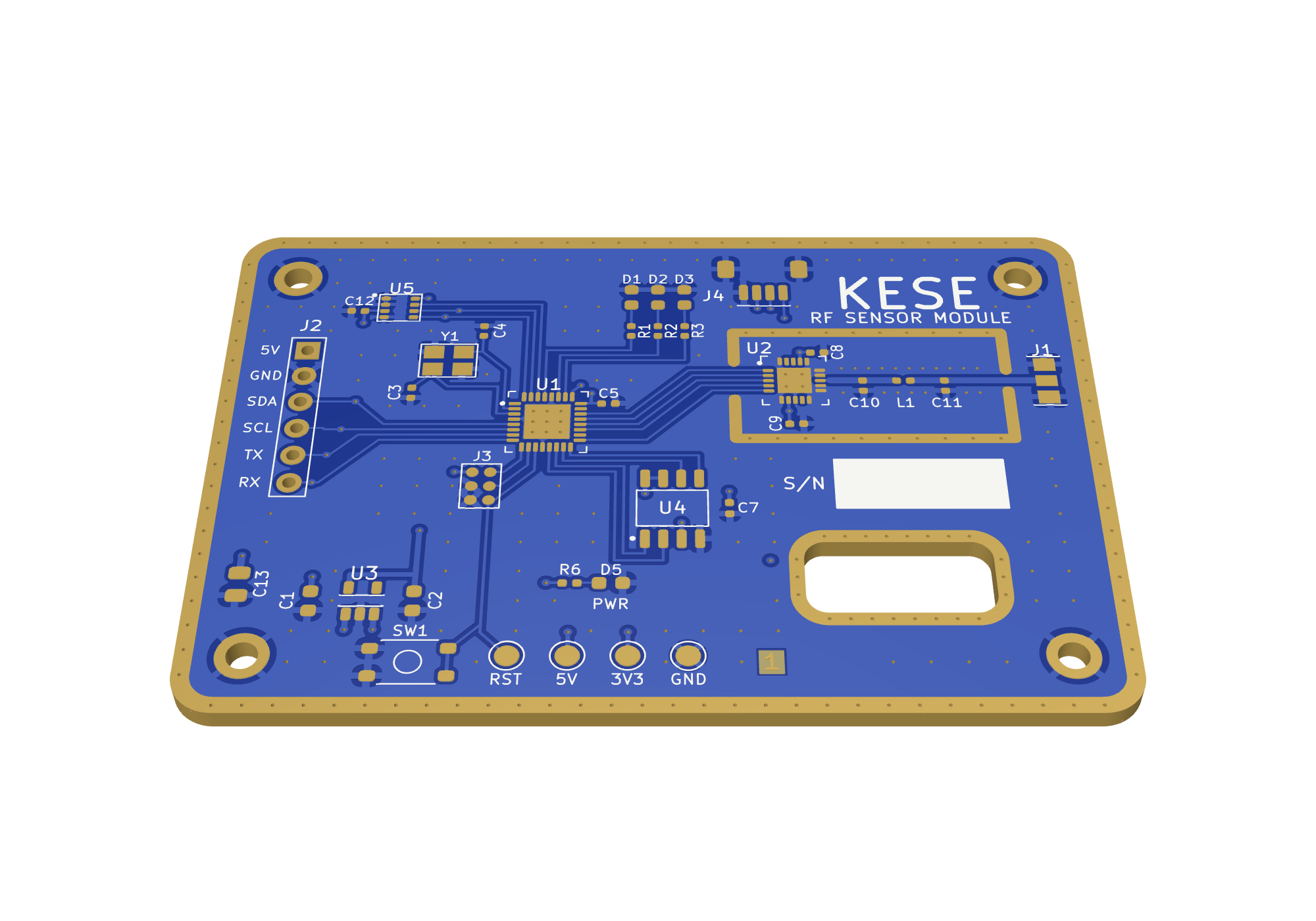
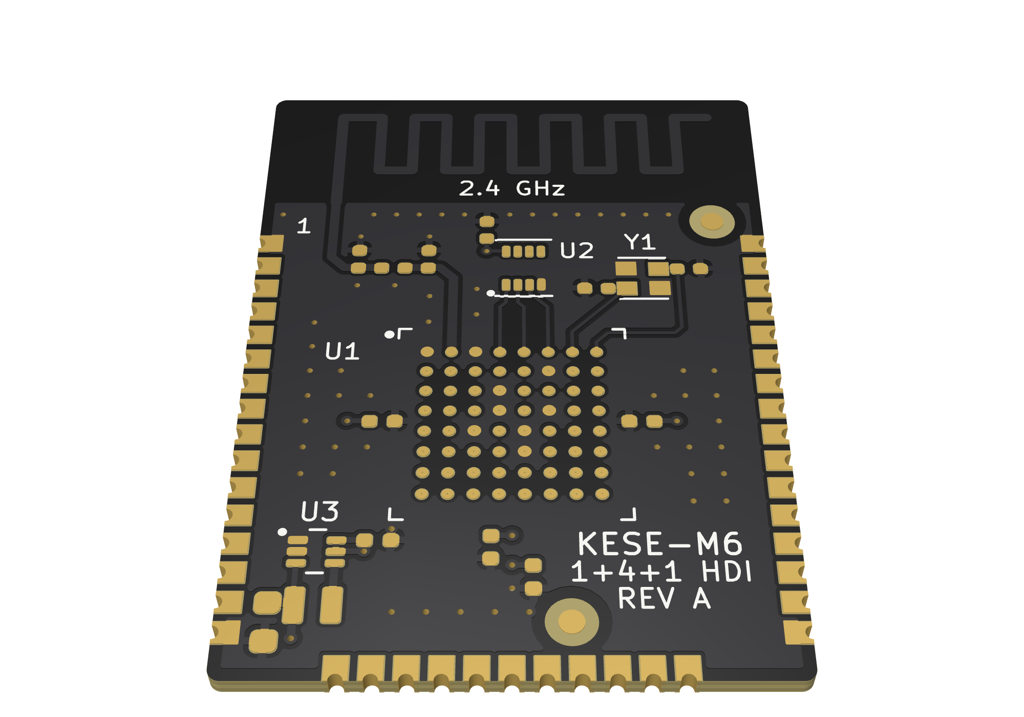
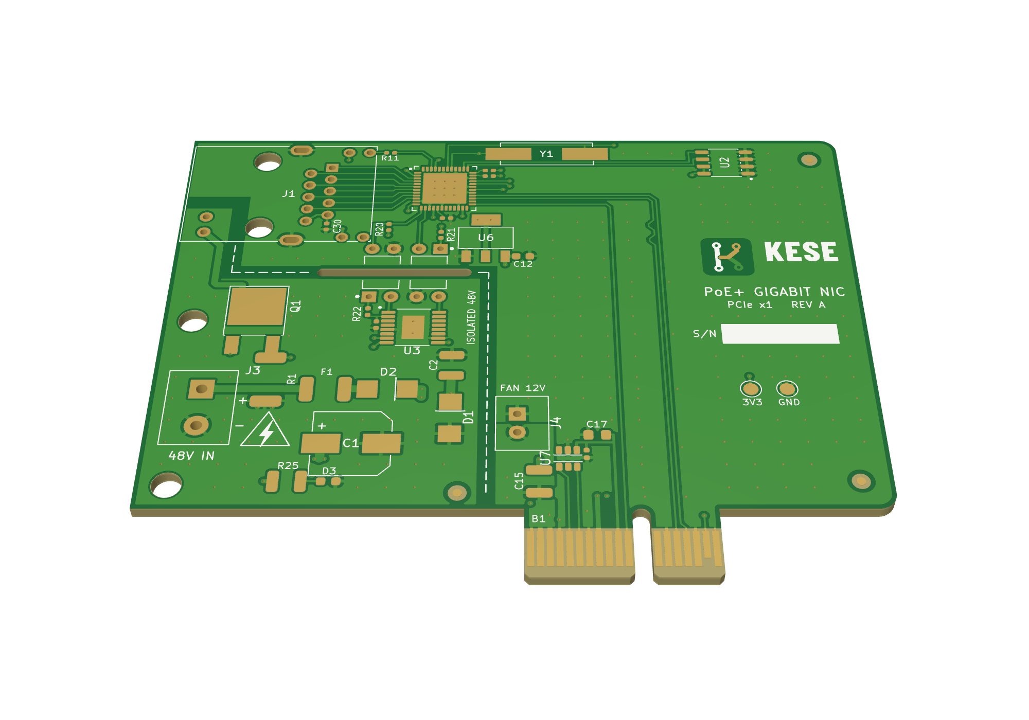
| RF sensor module | HDI radio module | PCIe x1 card | |
|---|---|---|---|
File in Input/
|
rf_module.kicad_pcb |
hdi_module.kicad_pcb |
pcie_card.kicad_pcb |
| Outline | 64 × 44 mm, a cut-out | 22 × 30 mm | 80 × 64.4 mm with the fingers' tongue, a slot |
| Thickness | 1.6 mm | 0.925 mm | 1.57 mm |
| Copper layers | 4 | 6, built 1+4+1 | 4 |
| Dielectrics | FR4: two prepregs of 0.2 mm, a core of 1.095 mm | prepregs 1067 and 1080, two IT-180A cores | two 2116 prepregs, an FR4 core of 1.01 mm |
| Vias | 307 through | 71 micro, 34 blind and buried, 45 through | 239 through |
| Board edge | plated all round and in the cut-out | 43 castellated pads | 36 gold fingers |
| Mask, silkscreen, finish | blue, white, ENIG | black, white, immersion silver | green, white, hard gold |
Simulation GLB with --verify
|
42 parts, 887,012 triangles; 21 s, 29.9 MB | 60 parts, 499,544 triangles; 14 s, 17.0 MB | 59 parts, 942,340 triangles; 19 s, 32.1 MB |
Simulation STEP with --verify
|
38 parts, 49 solids; 26 s, 225.0 MB | 56 parts, 58 solids; 15 s, 125.9 MB | 55 parts, 84 solids; 23 s, 215.3 MB |
Visual GLB with --verify
|
20 s, 17.1 MB | 15 s, 8.8 MB | 21 s, 18.3 MB |
The times are the ones the run prints, with the default parameters on one Linux machine with 4
cores. The STEP files were made with --for hfss --verify: millimetres and KiCad's origin, and,
as Run.STEP_WRITE_ROLES has it by default, no solder mask or silkscreen, so they have four parts
fewer than the GLB files (Project Capabilities gives
them with both). Read back with OpenCascade, every solid in them is valid and closed, and their
volume is the one the Verifier finds. The same three files are in featureTest/ as
21_rf_module, 22_hdi_module and 23_pcie_card, so the regression suite checks every part of
each in both modes (once: it skips the copies in Input/).
The pictures on this page are the boards' GLB files drawn with three.js. They were exported with
--set Run.COPPER_GROUPING=layer, so that the copper of each layer is one part and the layers
can be drawn apart; with the default grouping, one part per net, the boards look the same.
Input/rf_module.kicad_pcb: a 4-layer sensor board with a radio. A QFN-32 microcontroller with
its crystal, a 6-pad SWD connector and a SOIC-8 flash; a QFN-20 radio on an SPI bus, whose 50 Ω
line runs through a matching network to a coax connector between rows of stitching vias; an LDO
fed from a 6-pin header, three LEDs, test points on both sides and plated mounting holes. GND fills
F.Cu, In1.Cu and B.Cu, and In2.Cu is split into +3V3 and +5V.
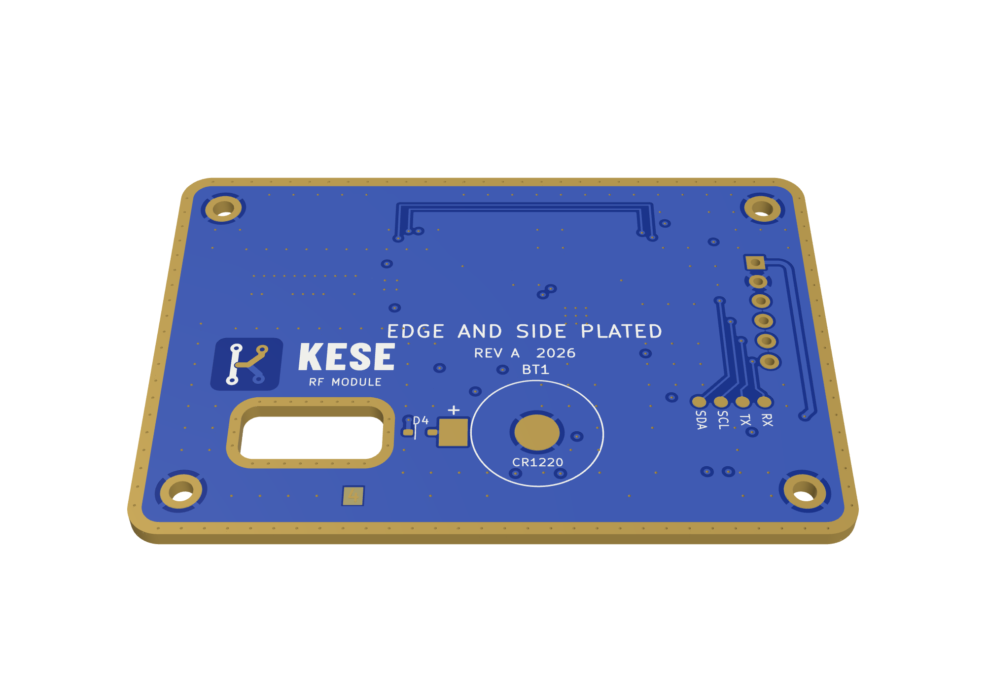
What this board shows:
-
A plated edge. The stack-up says
(edge_plating yes), so withCopper.EDGE_PLATING = "file"(the default) the routed edge is copper all round, and so are the walls of the 13 × 6 mm cut-out. The edge copper belongs to GND, the net with the most copper at the edge, and meets the GND border on every copper layer: 1.2 mm wide along the outline and 1.0 mm around the cut-out, the mask open over it, with a fence of GND vias in it. See Edge Plating. -
Its own stack-up. Every height comes from Board Setup: 35 µm outer and 17.5 µm inner copper, two FR4 prepregs and a core, a 1.6 mm board and a 10 µm mask. From
report.txt:stack-up copper layers: F.Cu, In1.Cu, In2.Cu, B.Cu laminate 1.5300 mm (stackup dielectrics (+ inner copper); board total in file 1.6 mm) F.Cu z +0.7650 .. +0.8000 mm (foil 0.035 mm) In1.Cu z +0.5475 .. +0.5650 mm (foil 0.0175 mm) In2.Cu z -0.5650 .. -0.5475 mm (foil 0.0175 mm) B.Cu z -0.8000 .. -0.7650 mm (foil 0.035 mm) dielectric 1 prepreg FR4 0.2000 mm er 4.5 tan d 0.02 z +0.5650 .. +0.7650 dielectric 2 core FR4 1.0950 mm er 4.5 tan d 0.02 z -0.5475 .. +0.5475 dielectric 3 prepreg FR4 0.2000 mm er 4.5 tan d 0.02 z -0.7650 .. -0.5650 -
Colours from the stack-up. The mask is KiCad's "Blue" and the silkscreen "White", so the mask parts come out

#14328C, over copper in visual mode
#3C5AB4, and the silkscreen
#F0F0EC(Colorizing). -
One part per net. 35 copper parts.
Copper_GNDis one closed solid made of the three planes, the border, the via fence, the plated edge and the barrels of its vias. The 50 Ω line isCopper_RFfrom the radio to L1 andCopper_RF2from L1 to the coax connector, each joined to its pads. -
The logo in three materials. On the back the KESE logo of
docs/logo/is bare copper, copper under the mask, and silkscreen. In visual mode the bare copper takes the exposed copper colour and the copper under the mask reads through it in the lighter blue. -
Keep-outs and finish. Three rule areas are counted under
skippedand make no copper, as intended. The stack-up's finish is ENIG; the finish is off by default, and--set Finish.FINISH_ENABLED=Trueadds the nickel and the gold on the bare copper (ENIG).
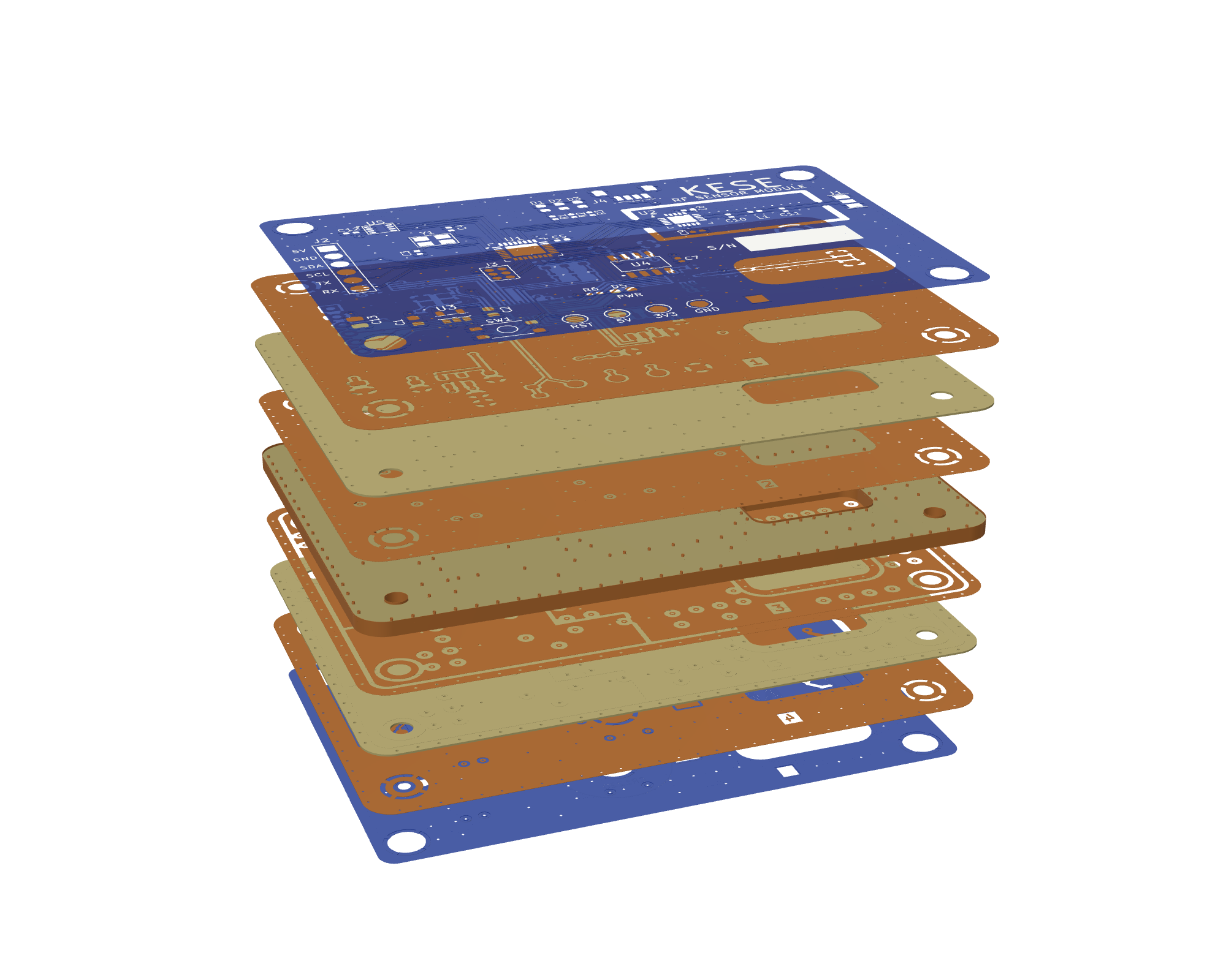
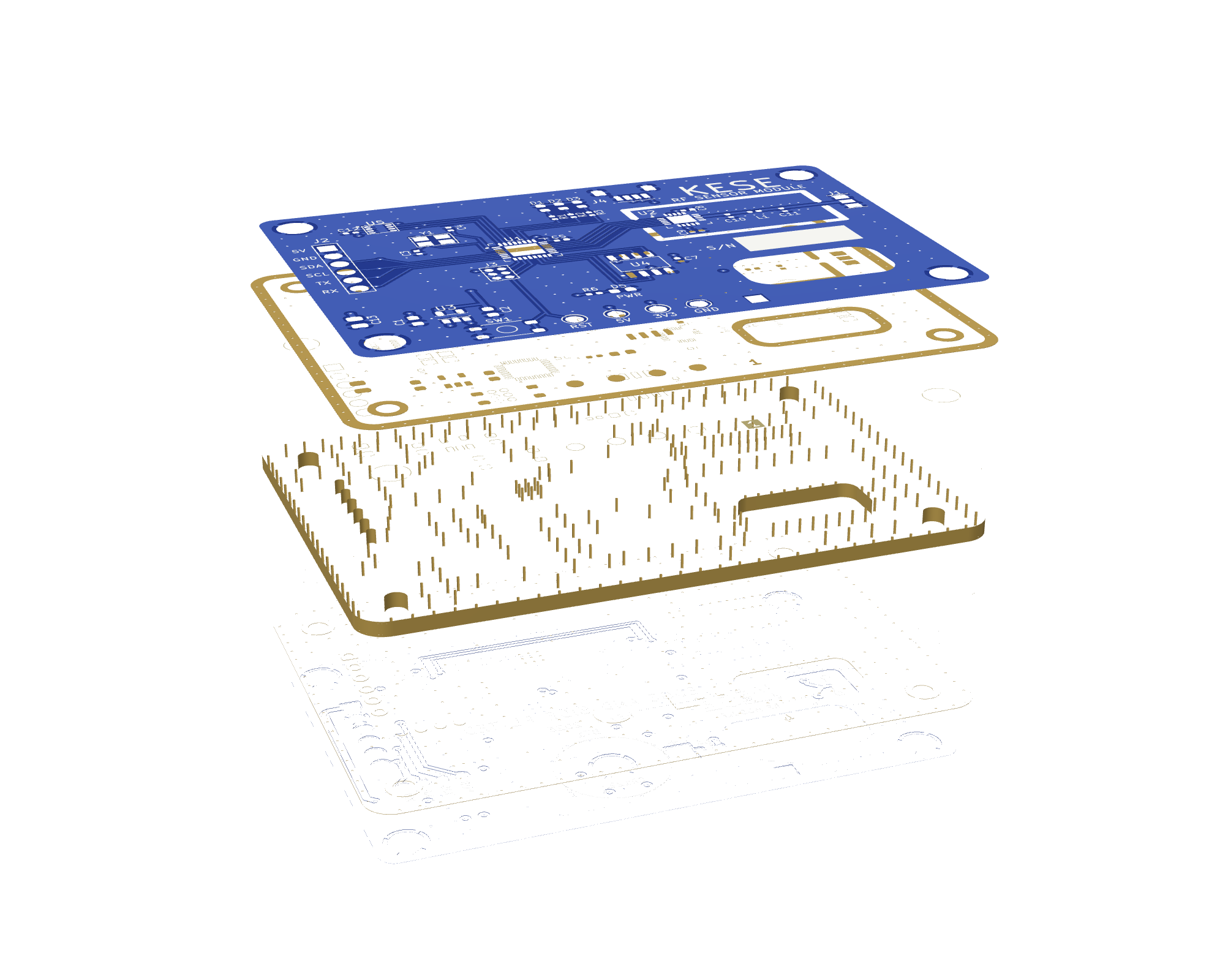
Left: simulation mode, every layer a closed solid. Right: visual mode, only the faces you can see.
| Part (simulation mode) | Triangles |
|---|---|
Copper_GND: the planes, the border, the via fence, the plated edge |
333,000 |
Copper_+3V3 and Copper_+5V: the two halves of In2.Cu, with their tracks and pads |
50,596 |
| the other 33 copper parts | 30,872 |
Board_dielectric 1 to 3
|
186,452 |
Top Solder Mask, Bottom Solder Mask
|
229,814 |
Top Silkscreen, Bottom Silkscreen
|
56,278 |
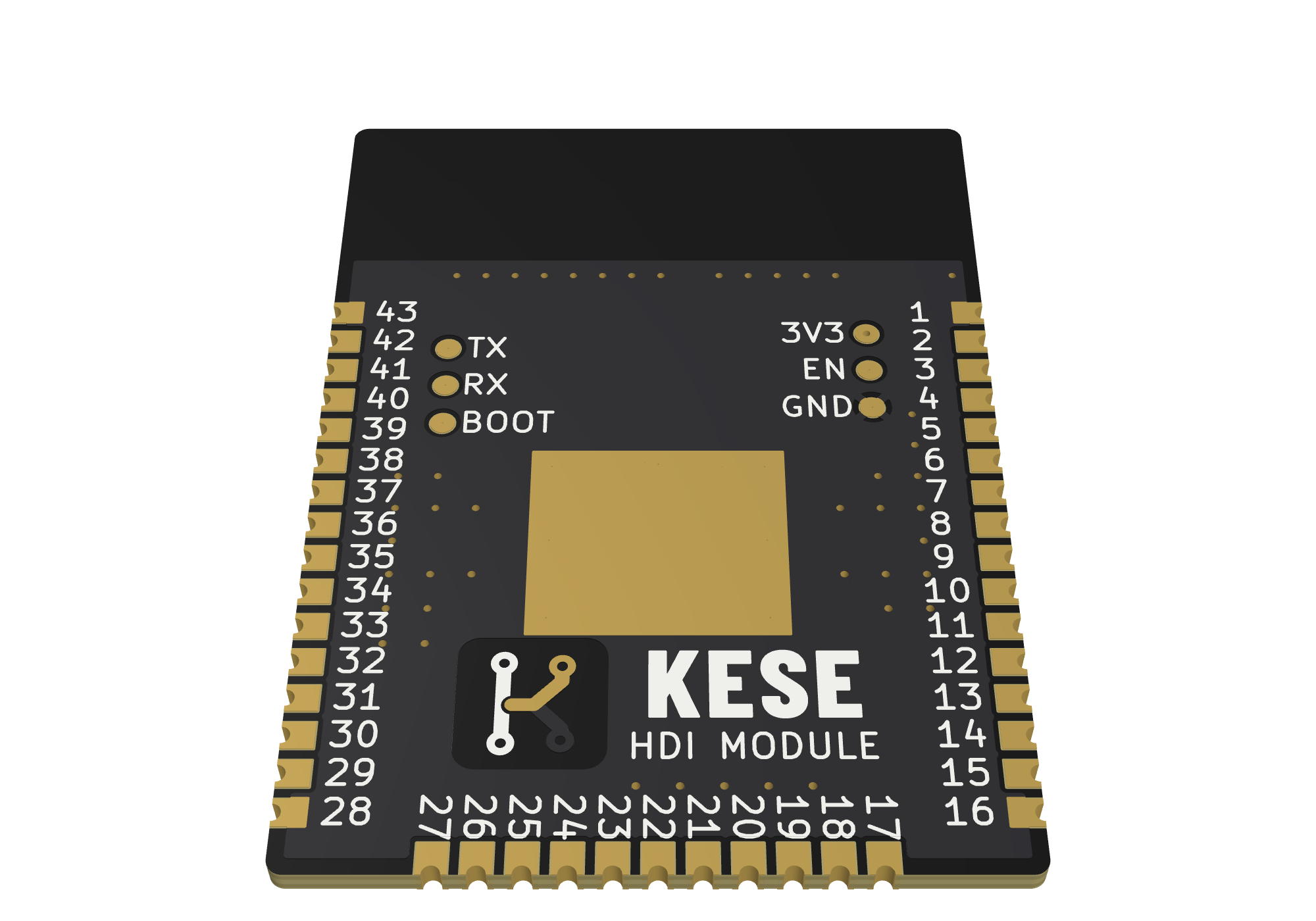
Input/hdi_module.kicad_pcb: a 6-layer radio module, built 1+4+1, one layer of microvias on each
side of a 4-layer core. A 64-ball BGA with a microvia in the pad of each inner ball and its
supplies on staggered buried vias, fanned out on In1.Cu to 43 castellated pads on three sides; a
USON-8 flash, a 2016 crystal, a buck converter making +1V1, and a matching network feeding a
meander antenna in a keep-out, its line referenced to In2.Cu through a cut in In1.Cu. GND on
In2.Cu, +3V3 on In3.Cu and a +1V1 island on In4.Cu; on the back an exposed GND pad, test pads
reached on In4.Cu, the pin numbers and the logo.
What this board shows:
-
Four kinds of via. 71 microvias, from each outer layer to the layer under it; 34 blind and buried vias, buried from In1.Cu to In4.Cu and blind from an outer layer to In2.Cu or In3.Cu; and 45 through vias. A via has its ring on the layers it spans and its barrel only between them (Vias And Plated Holes).
-
Named laminates. The dielectrics carry the glass styles and materials of the stack-up, each with its own εr and tanδ, and each becomes its own part,
Board_dielectric 1to5, with those values inmaterials.json(Material Properties):dielectric 1 prepreg 1067 0.0650 mm er 3.9 tan d 0.015 z +0.3525 .. +0.4175 dielectric 2 core IT-180A 0.2000 mm er 4.3 tan d 0.016 z +0.1350 .. +0.3350 dielectric 3 prepreg 1080 0.2000 mm er 4.0 tan d 0.016 z -0.1000 .. +0.1000 dielectric 4 core IT-180A 0.2000 mm er 4.3 tan d 0.016 z -0.3350 .. -0.1350 dielectric 5 prepreg 1067 0.0650 mm er 3.9 tan d 0.015 z -0.4175 .. -0.3525 -
Castellated pads. The 43 plated holes that the board edge cuts through are castellations: each drill notches the edge, and its plating is a part-barrel on the notch wall, joined to the pad's net (
Copper.CASTELLATION = "auto"; the file also says(castellated_pads yes)). See Castellated Holes. -
Keep-outs. The antenna's keep-out on every layer and the cut in In1.Cu under its line are rule areas: six of them, counted under
skipped, and no copper inside them. -
Black mask. The stack-up's "Black" gives

#121214, and over copper in visual mode
#2E2E30. The finish is immersion silver, built only withFinish.FINISH_ENABLED = True(ImmersionSilver).
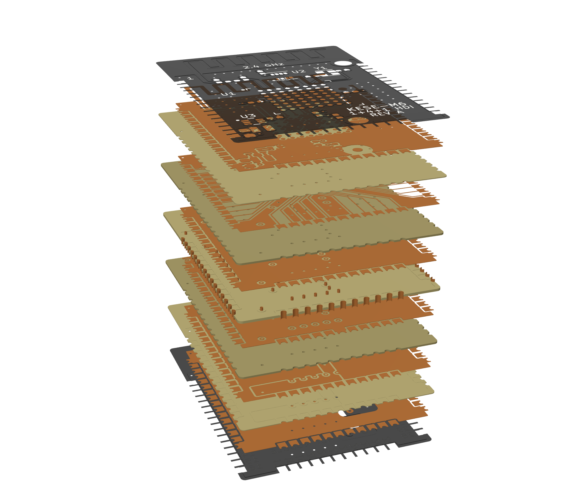
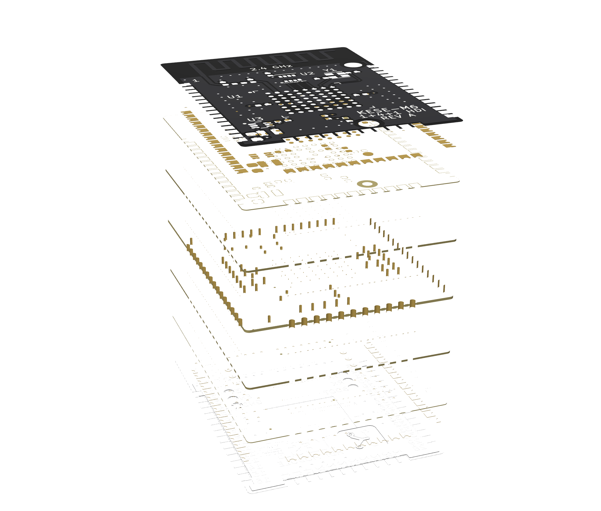
Left: simulation mode, every layer a closed solid. Right: visual mode, only the faces you can see.
Input/pcie_card.kicad_pcb: a 4-layer PCIe x1 gigabit Ethernet card that powers its port (PoE),
within a low-profile card's size (PCI Express CEM Rev 2.0: at most 68.90 mm from the bottom of the
fingers to the top, and 167.65 mm long). A QFN-48 controller with its crystal, EEPROM and +1V0
LDO; the PCIe lane and clock pairs length matched by meanders, with AC coupling capacitors on the
card's transmit pair; an RJ45 jack with magnetics at the bracket, a 12 V fan header and an SMBus
temperature sensor. Across a 2 mm band kept clear on every copper layer, and a slot, the PoE side:
48 V in through a fuse to a PSE controller switching the port through a MOSFET, its own PGND and
+48V planes, and optocouplers across the slot. GND on F.Cu, In1.Cu and B.Cu, +3V3 and a +1V0
island on In2.Cu. Where finger B1 sits from the bracket and the outline next to the bracket are
estimates.
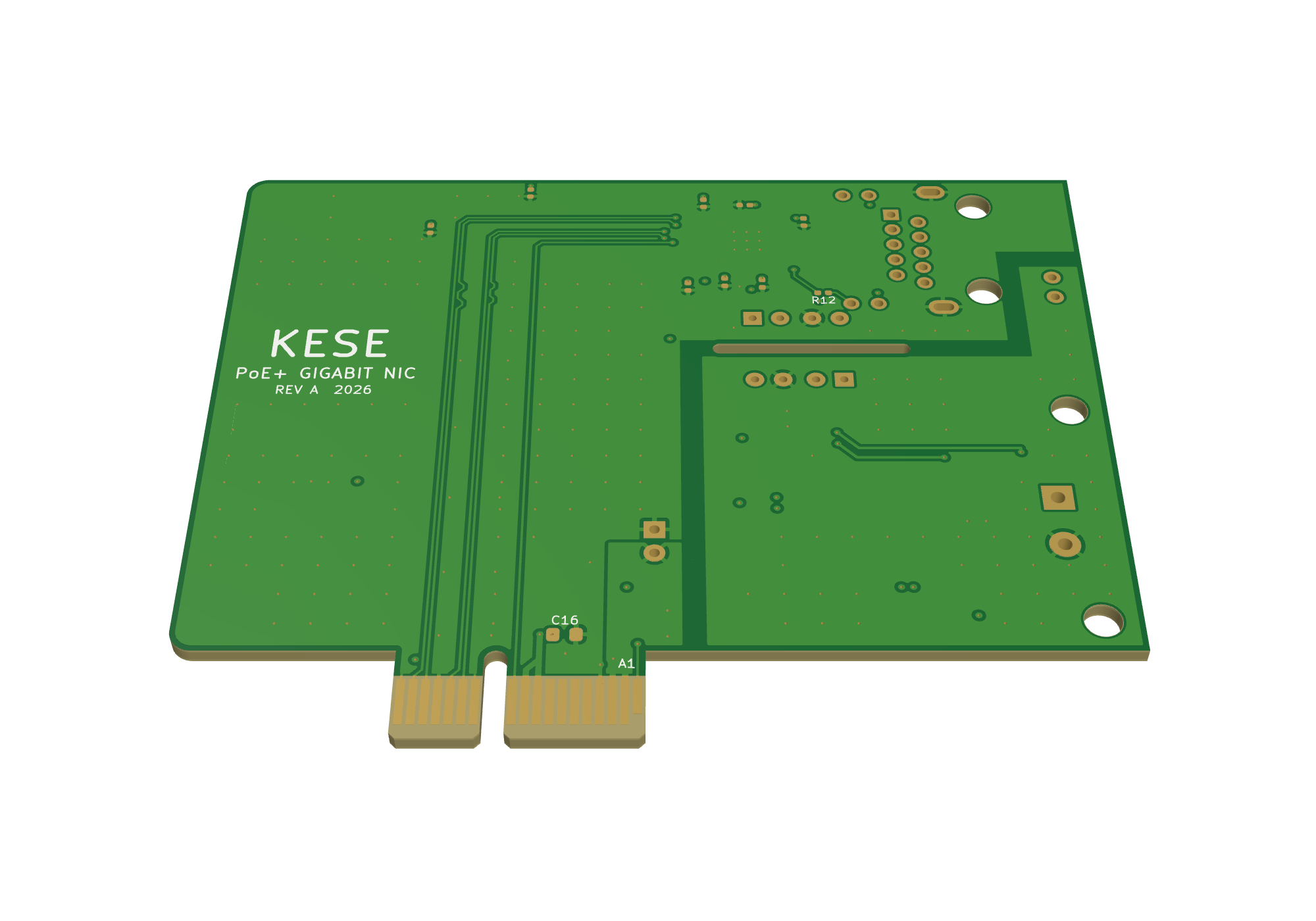
What this board shows:
-
Gold fingers. 18 fingers a side at a 1.00 mm pitch, side B on F.Cu and side A on B.Cu, on a
tongue with its key and its corners chamfered 0.5 mm at 45°. PRSNT1# and PRSNT2# are 1 mm shorter
and joined by a single trace, no plane runs under the fingers, and the mask is open over all of
them. Each finger is a pad of its net, so the lane pairs,
+12V,+3V3and GND end in the fingers. -
Hard gold. The stack-up's finish is hard gold. With
--set Finish.FINISH_ENABLED=Trueit covers all the exposed copper, fingers and pads alike, since KiCad gives a board one finish (HardGold). -
The bevel is not modelled. Board Setup's
(edge_connector bevelled)asks the fabricator to bevel the fingers' edge. KESE does not read it, so the card's edge stays square. -
An isolation barrier. A rule area 2 mm wide keeps every copper layer clear between the logic
side and the PoE side, and an 18 × 1.2 mm slot is milled through under it. The slot cuts every
layer, so
Copper_PGNDandCopper_+48Vstay apart from the logic side's parts. -
Planes per net.
Copper_GND(187,288 triangles),Copper_PGND(71,564),Copper_+3V3(37,072) andCopper_+48V(17,888) are the biggest of the 52 copper parts. - Non-plated holes. The bracket's two screw holes and the jack's two pegs are non-plated: their walls are bare laminate, with no plating and no ring.
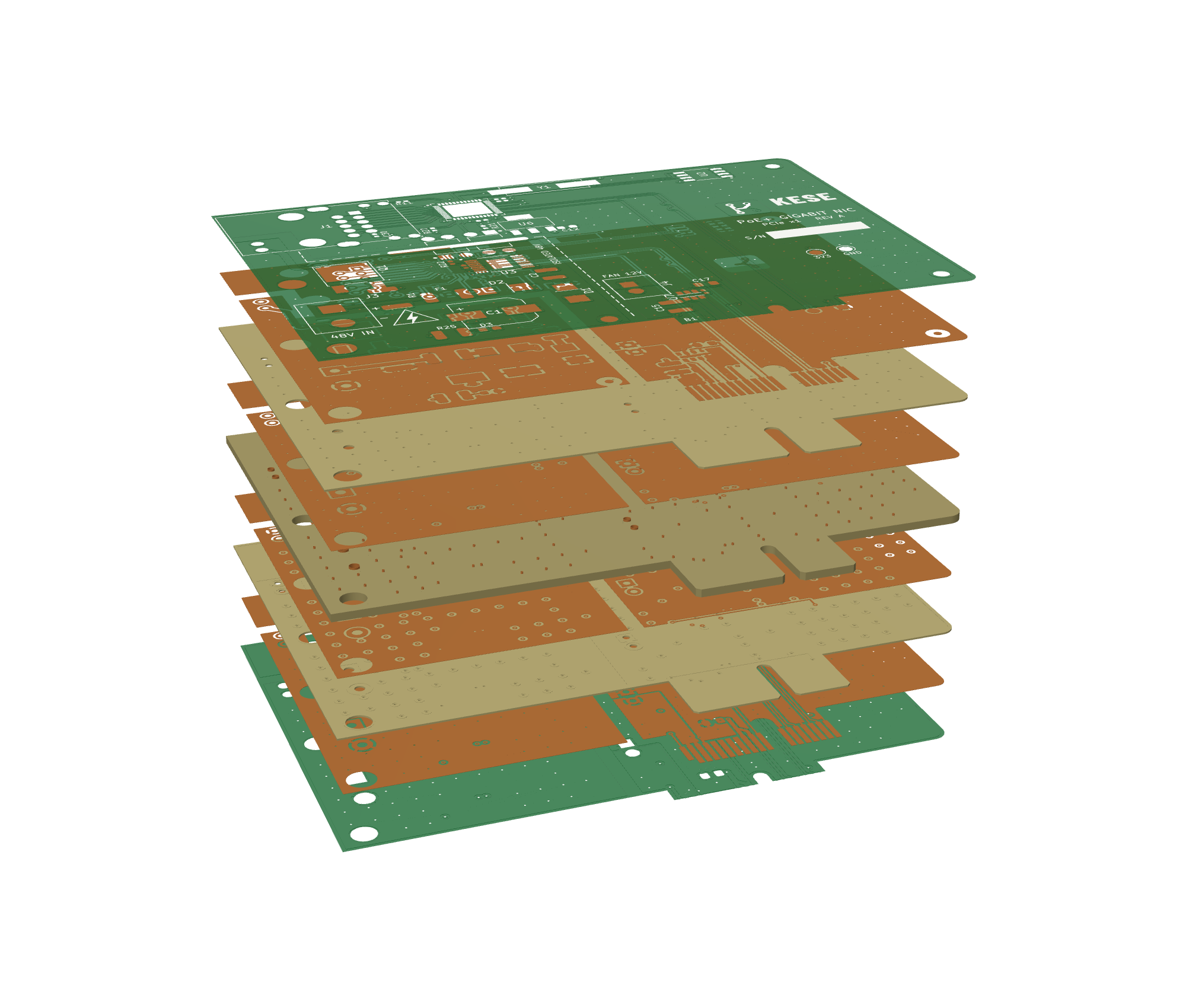
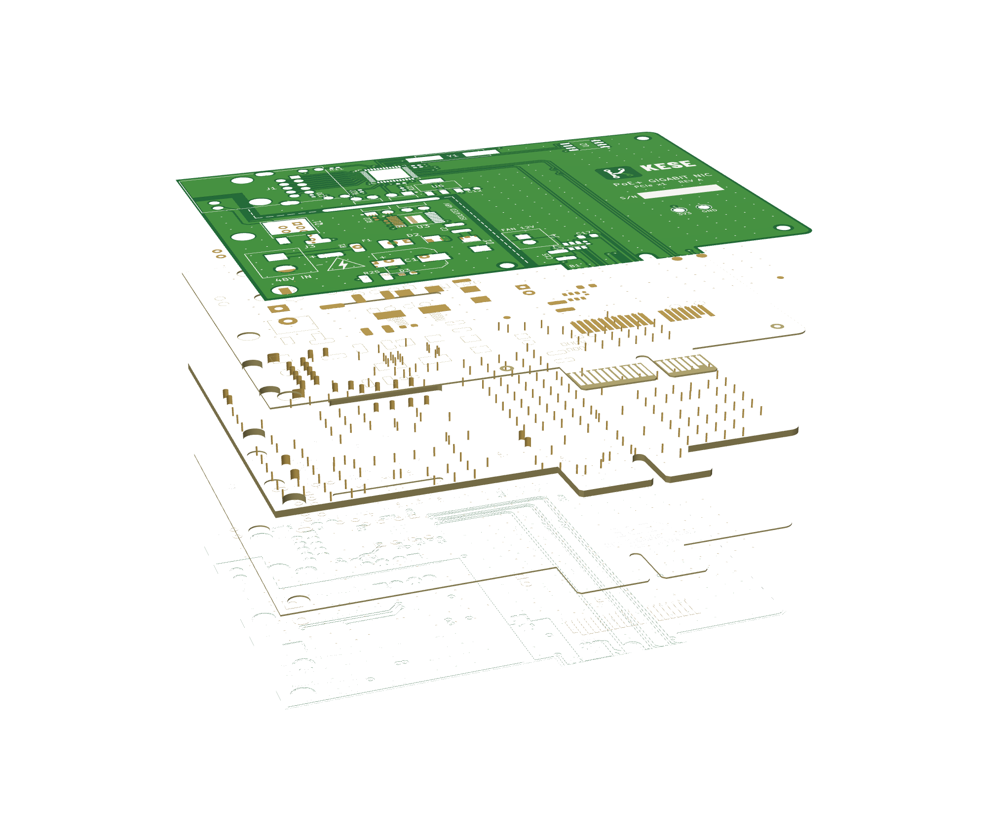
Left: simulation mode, every layer a closed solid. Right: visual mode, only the faces you can see.
cd Generator
python run_KESE.py                                                             # all three: simulation, GLB in metres, centred
python run_KESE.py Input/rf_module.kicad_pcb --for hfss                        # STEP in mm with KiCad's origin
python run_KESE.py Input/hdi_module.kicad_pcb --for viewer                     # visual mode for <model-viewer>
python run_KESE.py Input/pcie_card.kicad_pcb --set Finish.FINISH_ENABLED=True  # with the hard gold
python run_KESE.py Input/rf_module.kicad_pcb --set Run.COPPER_GROUPING=layer   # a copper part per layer
STEP files of these boards are large, 125 to 225 MB in mm, since every curve is written as flat faces: see Project Capabilities.
| Previous | Next |
|---|---|
| Project Capabilities | Working Principle |