Repository navigation
Solder Masks
The solder mask is the lacquer (LPI) over both faces of the board. kese/s4_geometry/solder_mask.py
builds it around the openings that kese/s3_resolve/mask.py works out; the settings are in
parameters/solder_mask.py. It is off by default (SolderMask.SOLDER_MASK_ENABLED = False): turn
it on to have it in the files. The openings still decide where the finish goes either way.
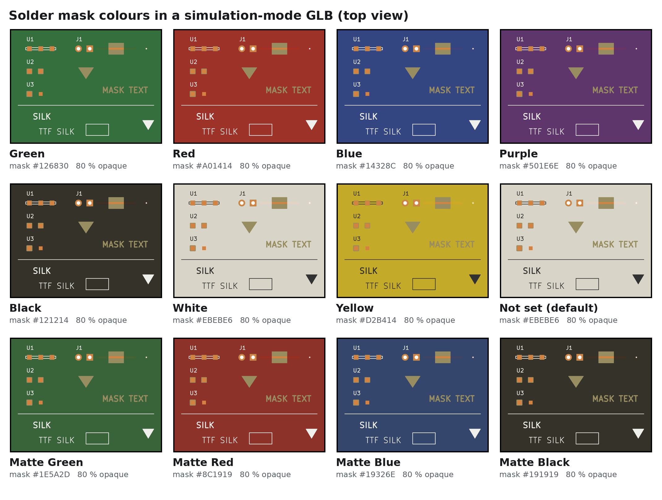
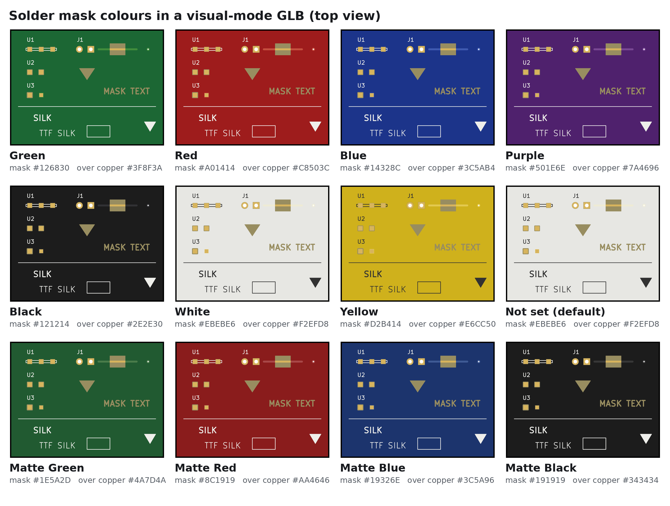
Whatever is drawn on F.Mask / B.Mask is an opening, not mask. KESE builds, per side:
| Symbol | Meaning | Parameter |
|---|---|---|
mask region on side F or B) |
||
| board outline, equation (11.3) | ||
| bores of every hole that reaches side |
||
| the mask openings on side |
||
| edge pull-back | SolderMask.MASK_EDGE_PULLBACK_MM |
The openings are:
| Opening | Size |
|---|---|
every pad that lists the mask layer (F.Mask, B.Mask, *.Mask) |
the pad shape grown by its mask margin: the pad's own solder_mask_margin, else the footprint's, else the board's pad-to-mask clearance, or SolderMask.PAD_TO_MASK_CLEARANCE_MM when set; a negative margin shrinks it at most to nothing (half its smaller side); a pad on no copper layer (a mask-only opening) is used as drawn, with no margin, as KiCad's PAD::GetSolderMaskExpansion does |
| every untented via (see via tenting) | the via pad grown by the same clearance: the board's, or SolderMask.PAD_TO_MASK_CLEARANCE_MM when set |
every track, arc track and copper drawing that the mask leaves bare (KiCad 9 and later: it lists both layers, (layers "F.Cu" "F.Mask"); only F.Cu is bared by F.Mask and B.Cu by B.Mask) |
its copper shape grown by its mask margin: its own solder_mask_margin, else the board's pad-to-mask clearance, or SolderMask.PAD_TO_MASK_CLEARANCE_MM when set. As in KiCad, a negative margin narrows a stroke at most to nothing; the opening of a filled polygon or square-cornered rectangle is never smaller than its inside, while a filled circle or rounded rectangle shrinks by the part of the margin past half its stroke (KiCad's EDA_SHAPE::TransformShapeToPolygon) |
| graphics, text and zone fills drawn on the mask layer | as drawn |
Together:
| Symbol | Meaning | Parameter |
|---|---|---|
|
|
a pad shape, a via pad, a shape drawn on the mask layer | |
|
|
the copper of a track or drawing the mask leaves bare, and its solder_mask_margin ( |
the board file |
| grows a region outward by |
||
|
|
the pad's and the footprint's solder_mask_margin
|
the board file |
| pad-to-mask clearance | board setup, or SolderMask.PAD_TO_MASK_CLEARANCE_MM when set |
Openings are clipped to the outline. report.txt counts pad mask openings on F.Mask, the bare
copper's openings (track mask openings on F.Mask, arc track ..., graphic ..., footprint graphic ...)
and the clearance used on its vias: line.
When the board sets a solder mask minimum width (Board Setup, (setup (solder_mask_min_width w)),
or SolderMask.MASK_MIN_WIDTH_MM), no web of mask narrower than plot_board_layers.cpp, GenerateLayerPoly): the
openings are grown by
Only the webs this fills are added; the hairlines where the grown and shrunk curves miss the exact
ones (narrower than 2 µm, twice SolderMask.MASK_WEB_HAIRLINE_MM) are left out, so the openings
keep their exact outlines. report.txt counts them as
mask webs under the min width (w mm) removed on F.Mask.
An opening narrower than 2 µm everywhere (twice SolderMask.MASK_OPENING_HAIRLINE_MM) is left out
too, the mask kept over it: the opening of a pad a micrometre across, which some boards place by the
hundred as markers, is no opening a fab makes, and the mask's edges around one at a pad's corner came
out a few tenths of a micrometre into the copper. report.txt counts them as
mask openings narrower than 0.002 mm left out on F.Mask.
The openings are worked on in groups: two openings within Parallel.WORKERS groups at a time in threads. The webs are the ones
the whole layer at once gives, with the same vertices, and the openings close the same region; on
CIAA ACC the front takes 4.3 s where the whole layer took 9.8 s.
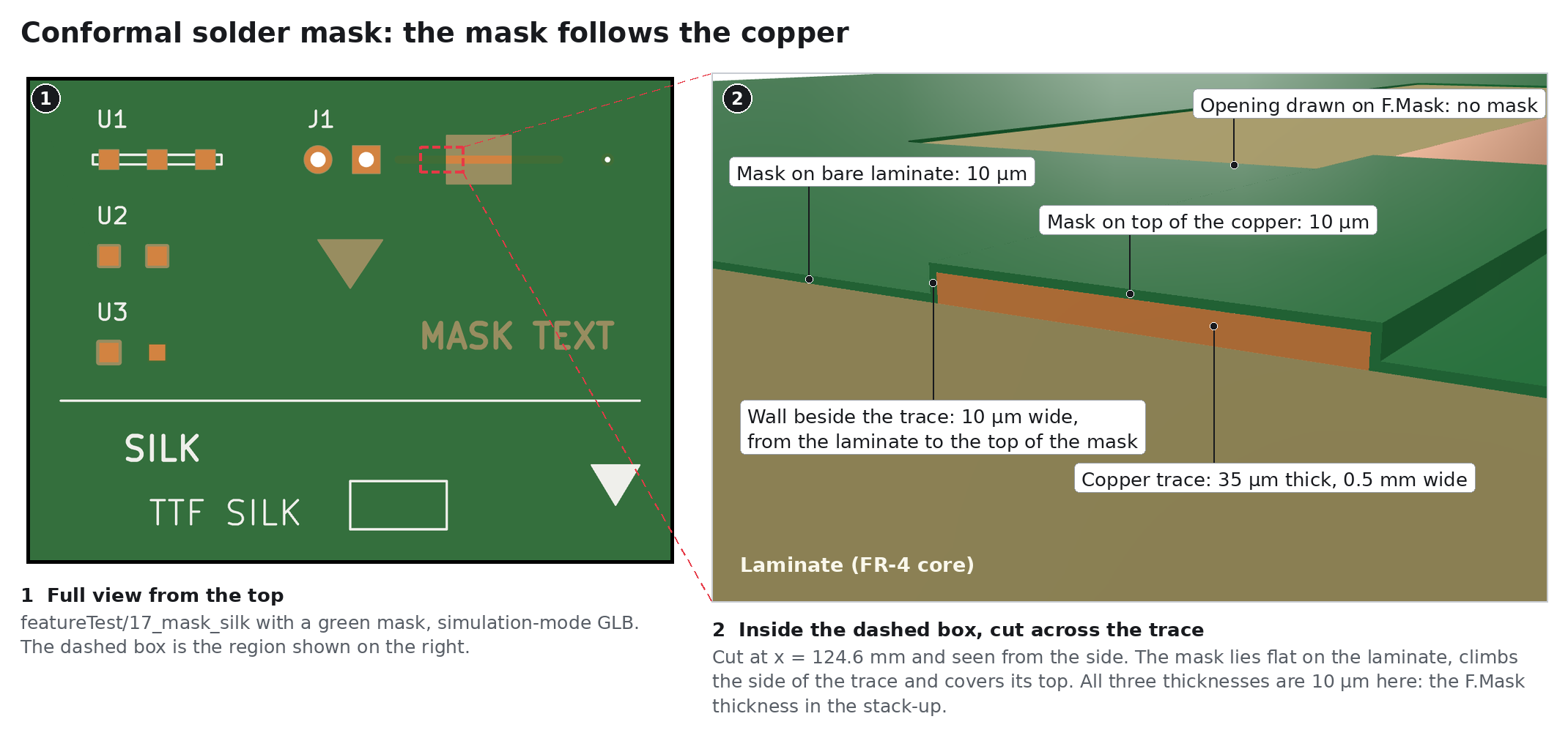
LPI mask follows the copper: it is thin on top of a trace and thicker on the bare laminate
beside it, and it climbs the side of every trace. KESE splits the mask region of equation (16.1)
into three regions with the outer copper
and extrudes them, on the F side, over
On the B side every z is mirrored (
| Symbol | Meaning | Parameter |
|---|---|---|
| mask on bare laminate, farther than |
||
| mask on top of copper | ||
| the band |
||
| all outer copper of side |
||
| mask thickness over laminate | SolderMask.MASK_OVER_LAMINATE_MM |
|
| mask thickness over copper | SolderMask.MASK_OVER_COPPER_MM |
|
| finished outer copper thickness, equation (8.3) | ||
| laminate thickness, equation (8.1) |
The wall's outer edge is rounded with MASK_WALL_QUAD_SEGS segments per quarter circle.
Where an opening's outline follows the copper's, as for a pad with no mask margin, the two seldom
match point for point: the opening's arc has other points than the pad's, or an edge rounds onto
the grid a step off. MASK_OVER_COPPER_HAIRLINE_MM (1 µm) everywhere is left out, and report.txt counts them:
solder mask: 8895 slivers on the copper narrower than 0.002 mm left out (F.Mask). Each is added
to the opening beside it, so the finish covers it as it covers the rest of the pad
(Finish), and no ink is printed on it
(Silkscreens), which would stand on mask that is not there.
The mask is worked out with its switch off too, so the finish reaches those pads' edges either way.
In simulation mode all three go into one part per side, Top Solder Mask / Bottom Solder Mask.
In visual mode the top region becomes its own part,
Top Mask over Copper / Bottom Mask over Copper, with its own colour
(Output Modes).
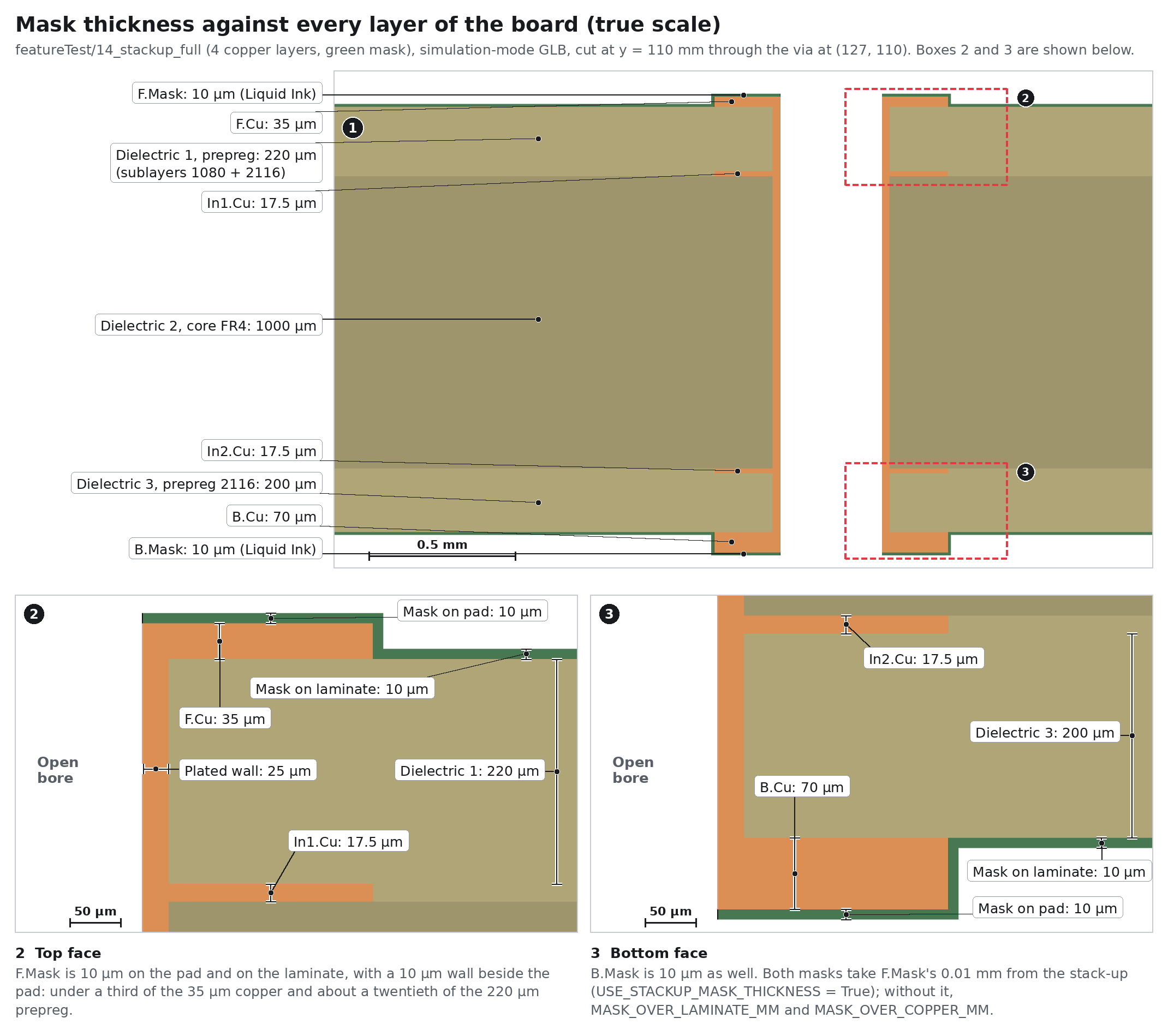
Two values, MASK_OVER_LAMINATE_MM and MASK_OVER_COPPER_MM, both 10 µm by default (KiCad's own
value). Typical production is 10 to 15 µm over copper and 20 to 30 µm over laminate. When the
stack-up gives a mask thickness and USE_STACKUP_MASK_THICKNESS = True, the first one in the
stack-up (normally F.Mask) is used for both values on both faces; a different B.Mask
thickness is ignored. report.txt notes the values and their source:
solder mask: 0.01 mm over laminate, 0.01 mm over copper (stackup).
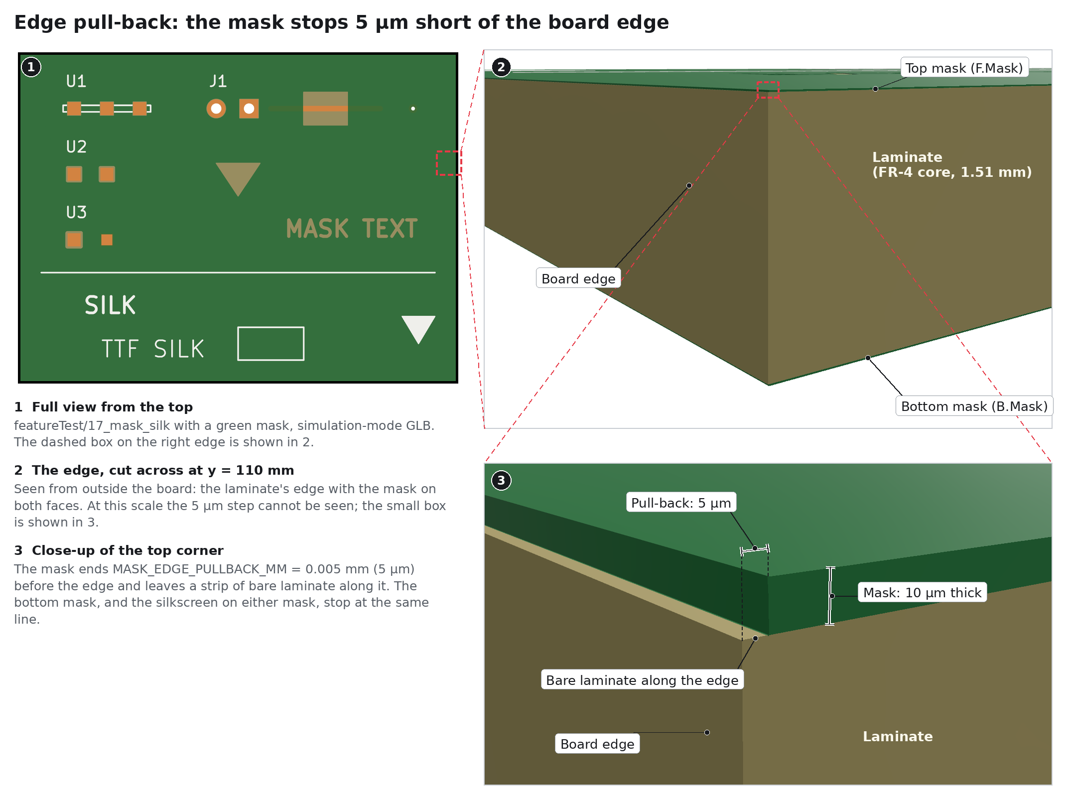
The mask, and the silkscreen on it, stop MASK_EDGE_PULLBACK_MM (5 µm) short of the board edge:
the <model-viewer>
from treating a translucent mask flush with the board edge as a baked shadow.
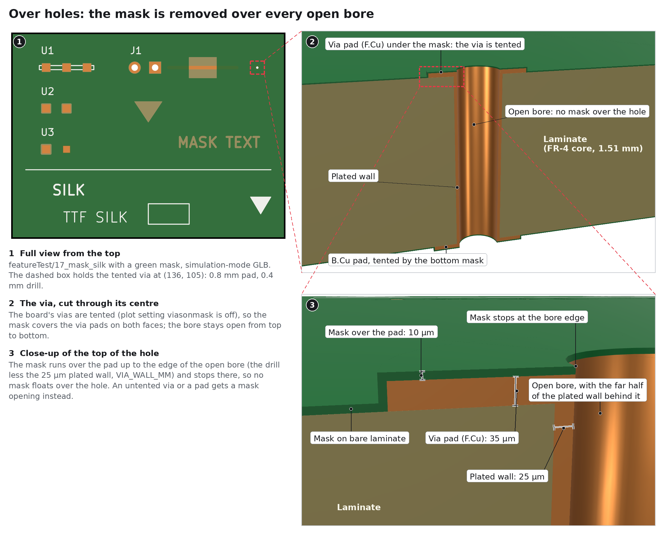
The mask is removed over the open bore of every hole that reaches that side (the drill minus the plated wall, or the whole drill of an NPTH), so no mask floats over a hole. A tented via keeps its mask over the annular ring; its bore is still open.
KiCad 10's via protection changes that (Copper And Traces): where a cap, a fill or a plug on that side shuts the bore, the mask of a tented via spans it; a covered via has the mask over its bore on that side even when its ring is left open, the opening then a ring around it. An end that a backdrill, counterbore or countersink opens stays open, and the copper a counterbore or countersink knocks out is a hole like any other.
| Name | Default | Range | Meaning |
|---|---|---|---|
MASK_OVER_LAMINATE_MM |
0.010 |
mm > 0 | Mask thickness over bare laminate |
MASK_OVER_COPPER_MM |
0.010 |
mm > 0 | Mask thickness on top of copper |
USE_STACKUP_MASK_THICKNESS |
True |
bool | The first mask thickness found in the stack-up (normally F.Mask's) wins, for both values on both faces |
MASK_EDGE_PULLBACK_MM |
0.005 |
mm ≥ 0 | Mask and silk stop this far from the edge |
PAD_TO_MASK_CLEARANCE_MM |
None |
None or mm ≥ 0 | Board-wide clearance around pads; None follows Board Setup. A pad's or footprint's own solder_mask_margin still wins |
MASK_MIN_WIDTH_MM |
None |
None or mm ≥ 0 | Narrowest web of mask kept between two openings, equation (16.2b); None follows Board Setup (solder_mask_min_width), 0 keeps every web |
MASK_WEB_HAIRLINE_MM |
1e-3 |
mm ≥ 0 | A web the minimum width adds that is narrower than twice this is dropped (16.2b) |
MASK_WALL_QUAD_SEGS |
4 |
int ≥ 1 | Curve quality of the walls beside traces |
MASK_OVER_COPPER_HAIRLINE_MM |
1e-3 |
mm ≥ 0 | A piece of mask on top of copper narrower than twice this is left out, and the finish covers it instead (16.2); 0 keeps every one |
MASK_OPENING_HAIRLINE_MM |
1e-3 |
mm ≥ 0 | A mask opening narrower than twice this everywhere is left out, the mask kept over it (16.2); 0 keeps every one |
| Previous | Next |
|---|---|
| Silkscreens | Parameter Reference |