Repository navigation
Board
The board is the laminate: the dielectric layers between and around the copper, with the
outline, the cut-outs and the holes. kese/s4_geometry/laminate.py builds it from the resolved
outline and stack-up; the settings are in parameters/board.py.
Each gap between two consecutive copper layers is one dielectric from the
Stack-Up Model: a core or a prepreg with its own thickness, material, εr
and tanδ. With Board.DIELECTRIC_GROUPING = "layer" (the default) each becomes its own part,
named Board_ plus the stack-up's name for that dielectric (Board_dielectric 1,
Board_dielectric 2, ... from the F.Cu side). A gap holds one part however many plies it has:
plies written as sub-layers of one stack-up dielectric keep that dielectric's name, and separate
stack-up dielectrics between the same two copper layers give one part named like
Board_dielectric 2 + dielectric 3. With "merged" every dielectric prism goes into
one part named Board.
Each dielectric prism is the outline minus every hole that passes through that gap: a via from
copper layer
With edge plating on (section 11.7 of Copper And Traces), the edge band
is also removed from every
| Symbol | Meaning |
|---|---|
| 2D region of dielectric |
|
| the board outline region (section 10.3) | |
| the drill of hole |
|
| index of the first and last copper layer hole |
|
|
|
region difference, union and intersection |
The prism is extruded over the z range of equations (7.8) and (7.9) in Stack-Up Model.
In materials.json, with "layer" grouping, every dielectric part carries kind (core /
prepreg), material, thickness_mm, epsilon_r, loss_tangent and between (the two copper
layers it separates). With "merged" the single Board part carries only the first dielectric's
values (its kind, thickness, εr, tanδ and between).
In a pressed laminate the resin of the prepreg flows into the spaces between the inner-layer
traces, so there is no air inside the board. KESE models this with
Board.RESIN_FILL_BETWEEN_INNER_COPPER = True (the default): for every inner copper layer, the
area of the outline that carries no copper on that layer, minus the holes through that
layer, is filled over the copper's own z band:
| Symbol | Meaning |
|---|---|
| resin-fill region beside inner copper layer |
|
| all copper of layer |
|
|
|
the copper band of |
With edge plating on, the edge band is also removed from
- the prepreg below the copper layer when the layer above is a core and the one below a prepreg;
- otherwise the dielectric above it.
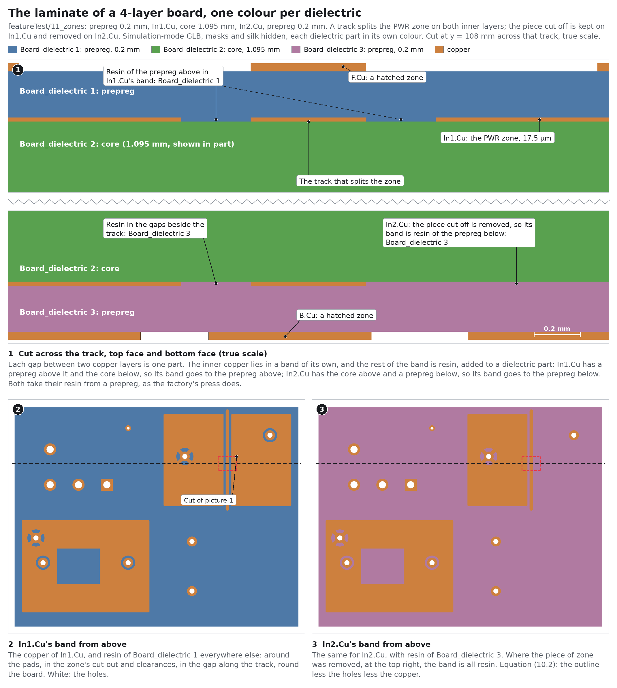
So both common 4-layer builds, prepreg-core-prepreg (as in the picture) and core-prepreg-core,
get their inner pockets filled from a prepreg, as in the factory. Inside KESE these prisms are tagged resin_fill_beside: <layer>; materials.json takes
a part's properties from its first prism, the dielectric slab itself, so the tag does not appear
there. With the setting
False, the pockets stay empty and report.txt notes it. With Board.DIELECTRIC_GROUPING = "merged" the fill goes into the single Board part.
Note
Where inner copper exists, dielectric k and dielectric k + 1 are separated by the copper band; the resin fill is what joins the laminate through the copper-free area of that band. Without it the laminate would be two separate solids touching only through copper.
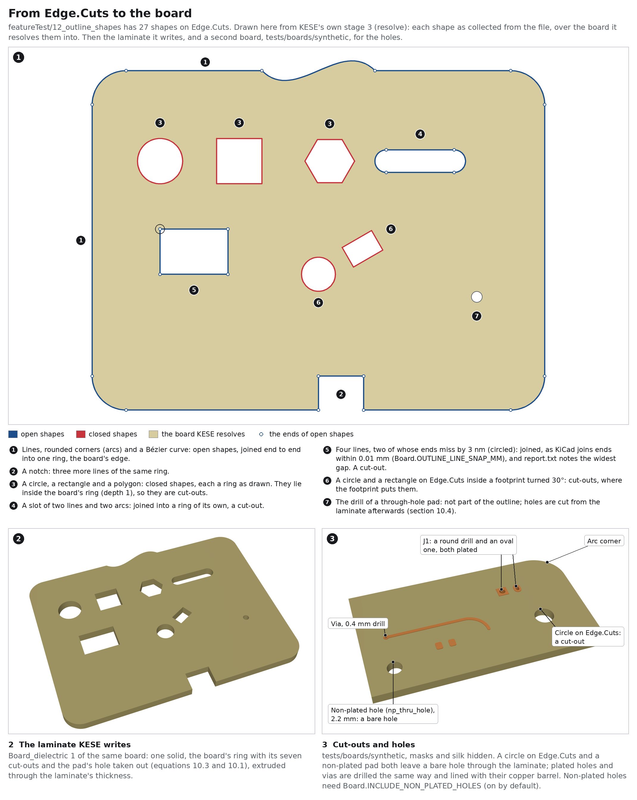
The outline comes from Edge.Cuts:
- Closed shapes (circles, rectangles, polygons) are taken as rings; a rectangle keeps its rounded
corners when it has them (KiCad 10,
(radius ...), at most half its shorter side, as in KiCad). - Open lines, arcs and Béziers are joined end to end the way KiCad chains them. An end that
meets no other end is moved onto the nearest other such end within
Board.OUTLINE_LINE_SNAP_MM(0.01 mm by default, KiCad's own chaining distance), the closest pairs first; ends that already meet stay where they are. The lines are then polygonized into faces. When a gap was closed this way,report.txtnotes the widest one. If the lines form no face at all, the run warnsEdge.Cuts lines/arcs do not form a closed outline. - Rings nested at an even depth are boards, rings at an odd depth are cut-outs. As in
KiCad, each cut-out is taken out of the ring one level up that holds it. A circle drawn inside
the outer outline is a hole through the whole board, and a ring drawn inside such a cut-out is a
board again, like a small board inside a panel frame (
featureTest/13b_outline_two):
| Symbol | Meaning |
|---|---|
| the board outline region | |
one closed ring found on Edge.Cuts
|
|
| a cut-out: a ring inside |
|
| how many other rings contain |
When Edge.Cuts gives no closed ring at all (nothing drawn, or only lines that do not close),
the fallback outline is
where Board.OUTLINE_FALLBACK_MARGIN_MM.
Board.OUTLINE_FALLBACK decides whether the fallback is used: "copper_hull" (the default)
uses equation (10.4) with "error" stops the run. When the lines do not
close but a closed shape (a circle, rectangle or polygon) is drawn on Edge.Cuts, there is no
fallback: that shape alone becomes the outline, even if it was meant as a cut-out.
Everything on every layer is clipped to the outline: copper, mask openings and silkscreen never reach past the board edge.
| Source | Hole | Setting |
|---|---|---|
| Via | drill of the via's (drill ...), spanning the via's layers |
plated, wall Copper.VIA_WALL_MM
|
Through-hole pad (thru_hole) |
the pad's drill, round or oval (slot), at the pad position; the drill's (offset ...) moves the copper pad, not the hole, as in KiCad |
plated, wall Copper.PTH_WALL_MM
|
Non-plated pad (np_thru_hole) |
the pad's drill | not plated; included when Board.INCLUDE_NON_PLATED_HOLES (default True) |
A plated hole leaves its barrel in the laminate: the dielectric is cut by the full drill and the copper barrel fills the ring between the drill and the drill minus the wall. See Copper And Traces for the plating.
Board.BOARD_THICKNESS_MM = None (the default) takes the laminate from the stack-up, or from the
file's (general (thickness ...)) less the outer copper and the two masks when there is no usable
stack-up (from 1.6 mm when the file gives no thickness either), so the finished board is KiCad's
board thickness. A number forces the laminate
thickness; see Stack-Up Model for how the dielectrics are scaled.
| Name | Default | Range | Meaning |
|---|---|---|---|
BOARD_THICKNESS_MM |
None |
None or mm > 0 | Laminate thickness; None takes it from the file |
DIELECTRIC_SPLIT |
"even" |
"even" |
How the laminate is divided when the file has no usable stack-up |
DEFAULT_DIELECTRIC_MATERIAL, DEFAULT_DIELECTRIC_TYPE
|
"FR4", "core"
|
text; "core" / "prepreg"
|
Material and type when the stack-up gives none |
DEFAULT_EPSILON_R, DEFAULT_LOSS_TANGENT
|
4.5, 0.02
|
> 0 | Typical FR4 at 1 GHz, used when the stack-up gives none |
USE_STACKUP_EPSILON_R, USE_STACKUP_LOSS_TANGENT
|
True, True
|
bool | Stack-up values win over the defaults when present |
RESIN_FILL_BETWEEN_INNER_COPPER |
True |
bool |
True: fill the space beside inner copper from the adjacent prepreg (otherwise from the dielectric above); False: those pockets stay empty and report.txt notes it (section 10.2) |
INCLUDE_NON_PLATED_HOLES |
True |
bool | NPTH pads become holes through the board |
OUTLINE_LINE_SNAP_MM |
0.01 |
mm > 0 | Open Edge.Cuts line and arc ends closer than this are joined, as KiCad joins them (its chaining distance is 0.01 mm) |
OUTLINE_FALLBACK |
"copper_hull" |
"copper_hull" / "error"
|
What to do when Edge.Cuts gives no closed ring at all |
OUTLINE_FALLBACK_MARGIN_MM |
1.0 |
mm ≥ 0 | Margin around the copper hull in the fallback |
| Previous | Next |
|---|---|
| Choosing An Export | Copper And Traces |