Repository navigation
Output Modes
KESE writes the same geometry in two modes, chosen with Run.MODE or --mode.
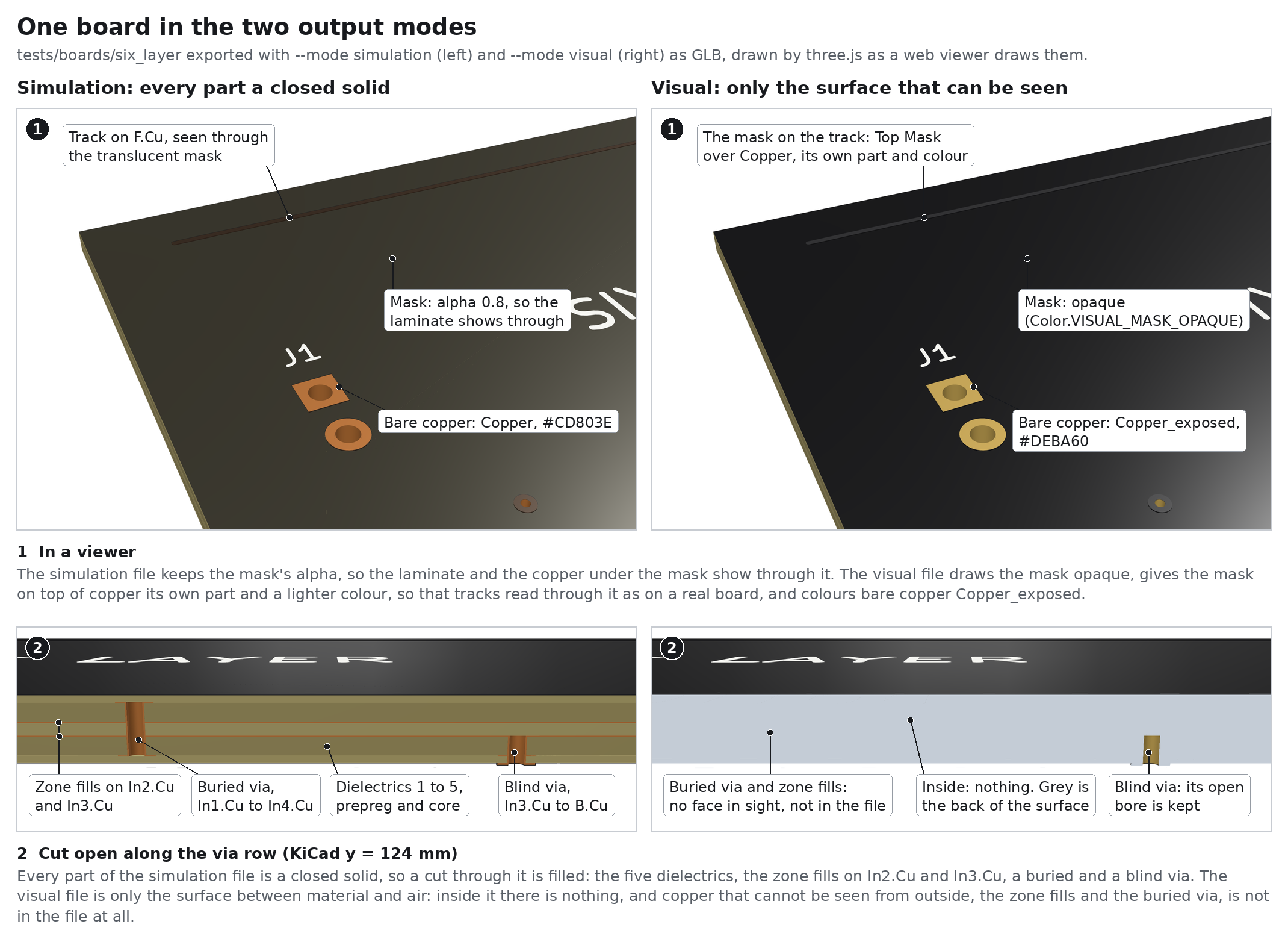
--mode simulation: the physical board as it leaves the factory. Every part is a closed solid:
each dielectric between two copper layers (core or prepreg), each net's copper with all of its
layers and vias joined into one body, via and hole plating, solder mask conformal over the copper,
silkscreen and, if enabled, the surface finish.
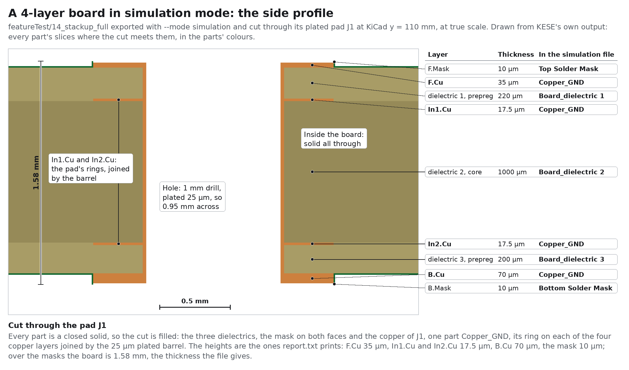
- Parts touch exactly (shared vertices, exact z values) and do not overlap, apart from the known exception listed in Working Principle; the Verifier checks that every part is closed, that its volume adds up and that no two parts overlap.
- All four formats are allowed: GLB, STEP, STL, OBJ.
- This is the mode for EM, SI / PI, thermal and mechanical solvers and for CAD.
Part names in simulation mode, with the default grouping:
| Role | Parts | Example |
|---|---|---|
board |
one per dielectric (Run.DIELECTRIC_GROUPING = "layer") or one Board ("merged") |
Board_dielectric 1 |
copper |
one per net (Run.COPPER_GROUPING = "net"), per layer ("layer"), or one Copper ("merged") |
Copper_GND, Copper_no_net
|
plating |
its own Plating part only with "layer" grouping; otherwise the barrels belong to the copper parts |
Plating |
mask |
Top Solder Mask, Bottom Solder Mask, each including the mask on top of copper |
|
silk |
Top Silkscreen, Bottom Silkscreen
|
|
finish |
per side and metal, or per side, metal and net |
Top Finish Gold, Top Finish Nickel_GND
|
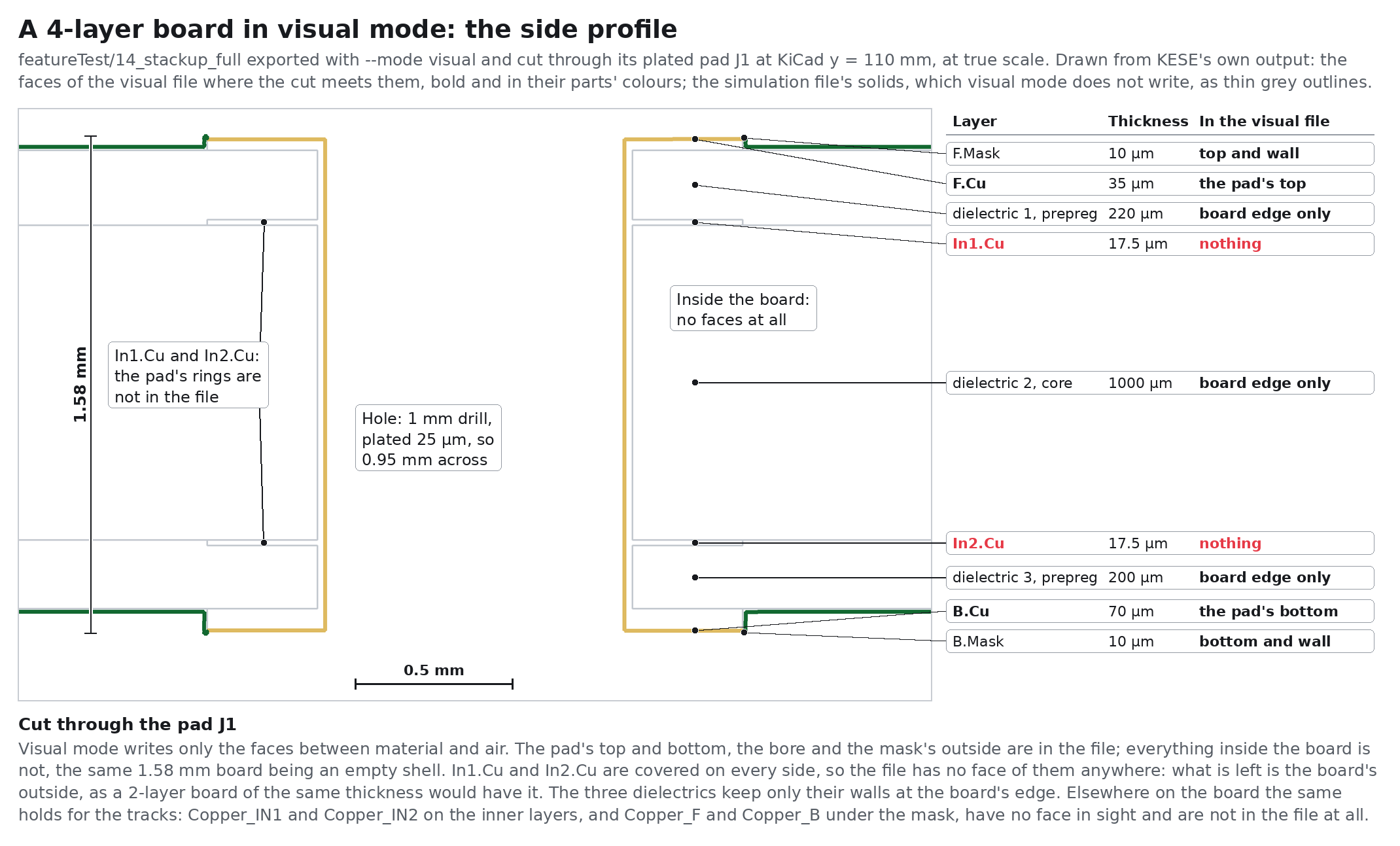
--mode visual: only the visible surface of the same geometry, for web viewers such as
<model-viewer> and three.js, and for renders. It is found in 2D, as the solids of simulation
mode are, but for all parts at once (kese/s6_assemble/skin_faces.py): at every height, a face
that looks up is one part's material below minus every part's material above, and a face that
looks down one part's material above minus every part's material below; a wall of a part is kept
where no other part's material stands against it. Where two parts meet, their touching faces are
never made, so what is left is the surface between material and air, every face still in the
part it came from. The faces are cut into triangles with their vertices shared across all parts
(skin_mesh.py), a big face strip by strip as in simulation mode, and two kinds of triangles are
then dropped:
- a triangle that looks at material across less than
$\varepsilon$ , two pieces that meet but for rounding, or a slit narrower than that:
| Symbol | Meaning | Parameter |
|---|---|---|
|
|
centre and outward unit normal of triangle |
|
| test offset (0.5 µm) | Geometry.SKIN_BURIED_TEST_OFFSET_MM |
|
| the probe point, |
||
| the two neighbouring heights of the model that |
||
| the material of every part between |
- the walls of a hollow sealed inside the board, such as the open bore of a buried via with nothing stacked on it: a closed shell that faces inward, which no one can see.
What remains is one outer surface, still split into named parts, closed but for the mouth of a
slit whose walls (8.1) took out (a crack well under a micron wide). A part with no face in
sight, such as the copper of a net that runs only on inner layers and through buried vias, has no
surface left and is not in the file. A finish thinner than
Why it exists: in the simulation model the mask lies on the copper and the copper on the laminate, with surfaces only microns apart. Viewers draw these with a depth buffer and the surfaces fight for the same pixels (z-fighting). The skin has no hidden surfaces, so nothing fights.
Differences from simulation mode:
- Only
glbandobjare allowed; asking forstlorstepis an error, because the skin is a surface, not solids. - The mask on top of copper becomes its own part,
Top Mask over Copper/Bottom Mask over Copper, with its own colour, so traces read through the mask the way they do on a real board. - The mask is drawn opaque whatever its alpha (
Color.VISUAL_MASK_OPAQUE), since a translucent surface with nothing behind it would look wrong. - All copper and plating take the
Copper_exposedcolour, since only bare copper is visible. - The parts are not closed solids: the Verifier's closed-solid and winding checks do not apply (the copper parts of the repository's boards even come out with negative signed volumes in the regression baseline), and it checks instead that along every vertical ray that hits the board the faces take turns, one going into the material and the next out of it: in, out on most rays, and in, out, in, out where a ray crosses a hollow open to the air, such as the bore of a buried via under stacked micro vias. A face left inside the material, or two faces in one place, gives two of a kind in a row.
| Need | Mode |
|---|---|
| HFSS, CST, openEMS, FEKO, COMSOL, any FEA or thermal solver | simulation |
| Mechanical CAD, checking the stack-up in a CAD viewer | simulation (STEP) |
| A web page, a product render, a Blender scene | visual |
| Smallest GLB of a dense board | visual (18.3 MB against 32.1 MB in simulation mode for the PCIe card example) |
The viewer preset (--for viewer) selects visual mode, GLB, metres and a centred origin in one
go. See Choosing An Export.
| Previous | Next |
|---|---|
| Stack-Up Model | Choosing An Export |