Repository navigation
Stack Up Model
The stack-up decides the height of every layer. It is read once per board
(kese/s2_collect/stackup.py), its heights are computed once (kese/s4_geometry/heights.py), and
it is printed at the top of report.txt, so every z value in the model can be checked against it.
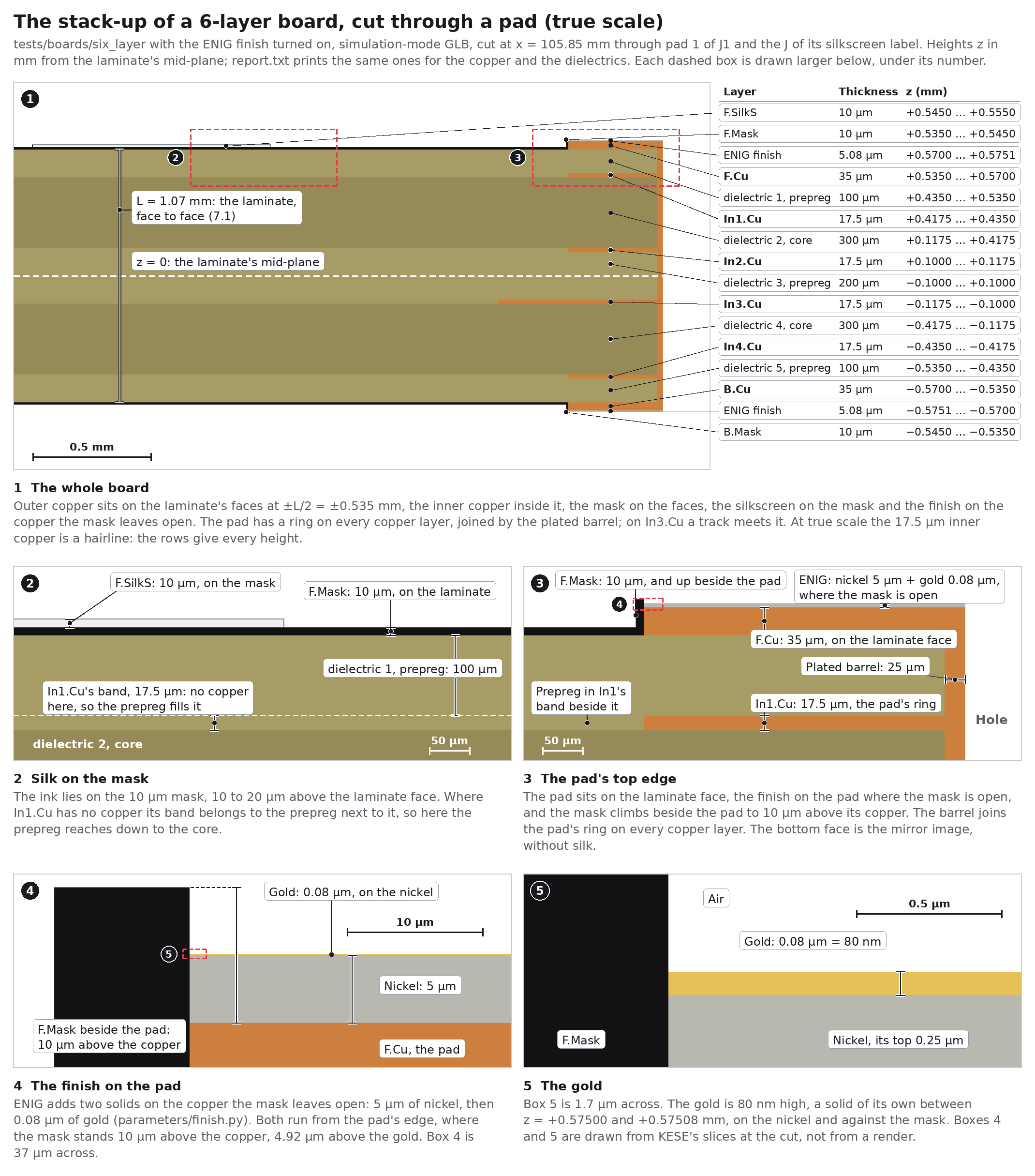
All heights are in mm, measured from the laminate mid-plane (F.Cu side
positive. A board has F.Cu
(B.Cu (
The laminate is the stack of dielectrics plus the inner copper layers:
| Symbol | Meaning | Unit |
|---|---|---|
| laminate thickness: dielectrics plus inner copper | mm | |
| thickness of dielectric |
mm | |
| foil thickness of inner copper layer |
mm | |
height of the laminate faces: F.Cu side, B.Cu side |
mm |
Outer copper sits on the laminate faces. Its finished thickness is the foil plus the plating added during hole plating:
| Symbol | Meaning | Parameter |
|---|---|---|
finished outer copper thickness (F.Cu, B.Cu) |
||
| foil thickness of the outer layer | stack-up, else Copper.DEFAULT_OUTER_FOIL_MM
|
|
| copper added to the outer layers by plating | Copper.OUTER_PLATING_ADDED_MM |
|
|
|
z range of the outer copper |
Inner copper lies inside the laminate. Walking down from the top face, each dielectric takes its thickness and each inner copper layer below it its foil thickness:
for every inner layer,
| Symbol | Meaning | Unit |
|---|---|---|
|
|
top and bottom of inner copper layer |
mm |
| thickness of dielectric |
mm | |
| foil thickness of inner copper layer |
mm |
Dielectric
The mask starts at the laminate face and the silkscreen lies on top of the mask; their heights are in Solder Masks and Silkscreens.
For a 6-layer board with 0.1 / 0.3 / 0.2 / 0.3 / 0.1 mm dielectrics, 17.5 µm inner foil and
35 µm outer foil (the tests/boards/six_layer.kicad_pcb board in the picture), equation (7.1) gives
In1.Cu at
report.txt shows:
  laminate 1.0700 mm (stackup dielectrics (+ inner copper); board total in file 1.2 mm)
  F.Cu     z +0.5350 .. +0.5700 mm  (foil 0.035 mm)
  In1.Cu   z +0.4175 .. +0.4350 mm  (foil 0.0175 mm)
  In2.Cu   z +0.1000 .. +0.1175 mm  (foil 0.0175 mm)
  In3.Cu   z -0.1175 .. -0.1000 mm  (foil 0.0175 mm)
  In4.Cu   z -0.4350 .. -0.4175 mm  (foil 0.0175 mm)
  B.Cu     z -0.5700 .. -0.5350 mm  (foil 0.035 mm)
  dielectric 1             prepreg  FR4        0.1000 mm  er 4.5  tan d 0.02   z +0.4350 .. +0.5350
  dielectric 2             core     FR4        0.3000 mm  er 4.5  tan d 0.02   z +0.1175 .. +0.4175
  ...
KiCad writes (setup (stackup (layer ...) ...)) once the stack-up has been confirmed in Board
Setup > Physical Stackup; a board whose stack-up was never set there has no such block (the
three example boards have one, featureTest/15_stackup_none has none). KESE reads, per layer:
| From the stack-up | Used for | Switch |
|---|---|---|
(thickness ...) of each *.Cu layer |
the foil thickness of that layer | Copper.USE_STACKUP_COPPER_THICKNESS |
(thickness ...), (type "core" / "prepreg"), (material ...), (epsilon_r ...), (loss_tangent ...) of each dielectric N layer |
one Dielectric per gap between copper layers |
Board.USE_STACKUP_EPSILON_R, Board.USE_STACKUP_LOSS_TANGENT
|
(thickness ...) of the first *.Mask layer that has one |
the mask thickness, over laminate and over copper | SolderMask.USE_STACKUP_MASK_THICKNESS |
(color ...) of F.Mask, B.Mask, F.SilkS, B.SilkS
|
the colours in GLB, OBJ and the look of materials.json, and in STEP when "mask" / "silk" are added to Run.STEP_WRITE_ROLES
|
Color.USE_STACKUP_COLORS |
(copper_finish "...") |
the finish type, when Finish.FINISH_ENABLED = True (off by default) |
Finish.FINISH_TYPE = "file" |
(edge_plating yes), (castellated_pads yes)
|
edge plating and castellations |
Copper.EDGE_PLATING = "file", Copper.CASTELLATION = "file"
|
A stack-up is usable when it has exactly one group of dielectric layers between every pair of
consecutive copper layers and every group has a thickness above zero. A gap made of several plies
(two prepregs, or prepreg + core + prepreg) becomes one dielectric solid with the summed
thickness and the first ply's type, material, εr and tanδ. Plies written as sub-layers of one
stack-up dielectric keep that dielectric's name (dielectric 3 in six_layer); separate stack-up
dielectrics in one gap give a joined name (dielectric 1 + dielectric 2):
| Symbol | Meaning |
|---|---|
| thickness of the dielectric solid in gap |
|
| number of plies in gap |
|
| thickness of ply |
The laminate thickness is then equation (7.1). The file's (general (thickness ...)) is not used
when a usable stack-up is present; report.txt only shows it as board total in file. (KiCad computes
that number from the stack-up as all copper + all dielectrics + both masks, so for a stack-up
saved from Board Setup it equals the laminate plus the two outer foils and the two masks.)
Any value the stack-up leaves out falls back to the parameter defaults:
Copper.DEFAULT_OUTER_FOIL_MM, Copper.DEFAULT_INNER_FOIL_MM, Board.DEFAULT_DIELECTRIC_MATERIAL,
Board.DEFAULT_DIELECTRIC_TYPE, Board.DEFAULT_EPSILON_R, Board.DEFAULT_LOSS_TANGENT,
SolderMask.MASK_OVER_LAMINATE_MM / MASK_OVER_COPPER_MM.
When the file has no stack-up block, or an unusable one:
- The laminate thickness is the file's
(general (thickness ...)), or 1.6 mm (Board.DEFAULT_BOARD_THICKNESS_MM) when the file has none, less the outer copper and the two masks (SolderMask.MASK_OVER_COPPER_MMeach), as KiCad's default stack-up counts them (BOARD_STACKUP::BuildDefaultStackupList), so the finished board is KiCad's board thickness, equation (7.10b). - The laminate minus the inner copper is divided evenly between the copper layers
(
Board.DIELECTRIC_SPLIT = "even", the only split implemented), equation (7.11). Each gap becomes a dielectric nameddielectric 1,dielectric 2, ... of the default type and material with the default εr and tanδ. - Copper layers without a thickness in the file get the default foil thickness (an unusable stack-up block may still supply some).
| Symbol | Meaning | Parameter |
|---|---|---|
| thickness of every dielectric | ||
| laminate thickness, equation (7.10b) | ||
the file's board thickness, else Board.DEFAULT_BOARD_THICKNESS_MM (1.6 mm) |
(general (thickness ...)) |
|
|
|
foil of the outer copper layers | Copper.DEFAULT_OUTER_FOIL_MM |
| mask thickness over copper | SolderMask.MASK_OVER_COPPER_MM |
|
| foil of inner copper layer |
Copper.DEFAULT_INNER_FOIL_MM |
|
| number of copper layers |
The 4-layer featureTest/15_stackup_none has no stack-up and a 1.2 mm board:
Board.BOARD_THICKNESS_MM (default None) overrides the laminate thickness. With a usable
stack-up the dielectric thicknesses are scaled so their proportions are kept; without one the
even split of equation (7.11) is applied to the forced value:
| Symbol | Meaning | Parameter |
|---|---|---|
| forced laminate thickness | Board.BOARD_THICKNESS_MM |
|
| dielectric thickness from the stack-up | ||
| dielectric thickness used | ||
| scale factor |
report.txt states the source on the laminate line:
report.txt says |
Meaning |
|---|---|
stackup dielectrics (+ inner copper); board total in file X mm |
summed from the stack-up |
file (general (thickness T)) less the outer copper and the masks - no usable stackup |
the file's board thickness less outer copper and masks, split evenly |
default 1.6 mm less the outer copper and the masks (no thickness in file) |
neither was available |
Board.BOARD_THICKNESS_MM (... (stackup dielectric proportions kept)) |
forced by the parameter |
Important
KiCad's defaults (35 µm copper on every layer, 10 µm mask, εr 4.5, tanδ 0.02) are what you get
when the stack-up is missing. They are typical, not your fabricator's. For lab work, enter the
fabricator's stack-up in KiCad's Board Setup or set the defaults in parameters/.
| Feature | Height used |
|---|---|
| Dielectric |
equations (7.8) and (7.9) |
| Resin beside inner copper | the inner copper's own band, filled from the adjacent prepreg, else from the dielectric above (box 2 of the picture; Board) |
| Copper of layer |
its band, equations (7.4) to (7.7) |
| Via barrel from layer |
between the copper layers it joins; outer copper caps it, inner copper is drilled through, so the barrel passes through inner bands (Copper And Traces) |
| Solder mask | from the laminate face: mask thickness over laminate, copper + mask thickness over copper (Solder Masks) |
| Silkscreen | on top of the mask surface (Silkscreens) |
| Surface finish | stacked on top of the outer copper where the mask is open (boxes 4 and 5 of the picture; Top And Bottom Copper Finishings) |
| Previous | Next |
|---|---|
| Working Principle | Output Modes |