Repository navigation
Tombstone and Shield Mod
Applies to: zBitx v1 hardware only. zBitx v2 has improved isolation and does not need this mod.
The tombstone and shield modification is a hardware improvement for the original zBitx v1. It reduces spurious emissions, digital noise coupling, and unwanted mixing products.
It combines two techniques:
- Tombstoning two components near the Si5351 to reduce PCB coupling and stray capacitance
- Shielding the nearby coils to isolate them from the noisy digital and oscillator circuitry
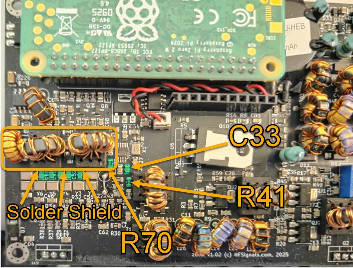
On the zBitx v1, high-speed digital circuitry (Raspberry Pi, Si5351 clock generator, display) sits close to sensitive RF stages. This can cause:
- Spurs from Si5351 mixing products
- Broadband noise from digital switching
- Noise coupling into the IF and RF paths
- Degraded spectral purity at lower output power
Tombstoning and shielding reduce the parasitic coupling paths and contain radiated noise.
Tombstoning means mounting a surface-mount part on end (vertically) instead of flat on the board, so only one end touches a pad. This reduces capacitive coupling to the ground plane, removes unwanted RF paths, and improves isolation at sensitive nodes.
Shielding means placing a grounded conductive barrier around a noise source or a sensitive RF section.
- Fine-tip soldering iron
- Tweezers and magnification
- Snips or Wire Cutters
- Short lengths of thin wire for jumpers
- Copper tape or thin copper/brass sheet
- Kapton tape for insulation
- Multimeter with continuity mode
Disconnect power and remove the battery before you begin.
- Locate R70 near the Si5351.
- Desolder R70.
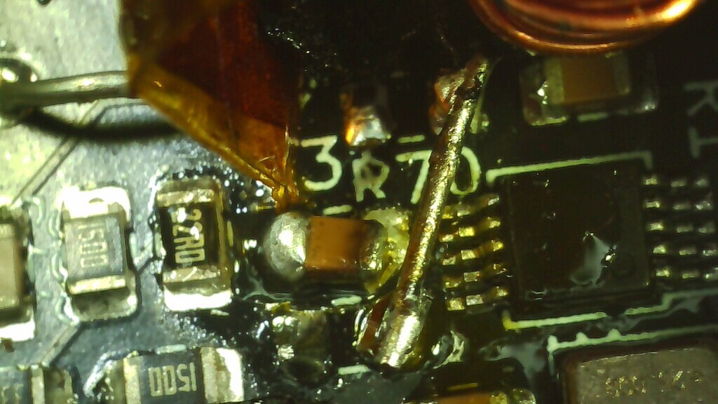
- Stand it on end and solder it to the pad closest to the Si5351.
- Locate C33 near the Si5351.
- Desolder C33.
- Stand it on end and solder it to the pad closest to the Si5351.
Connect the free (upper) ends of R70 and C33 with a short piece of wire.
Keep this jumper as short as possible. Long leads can act as antennas.
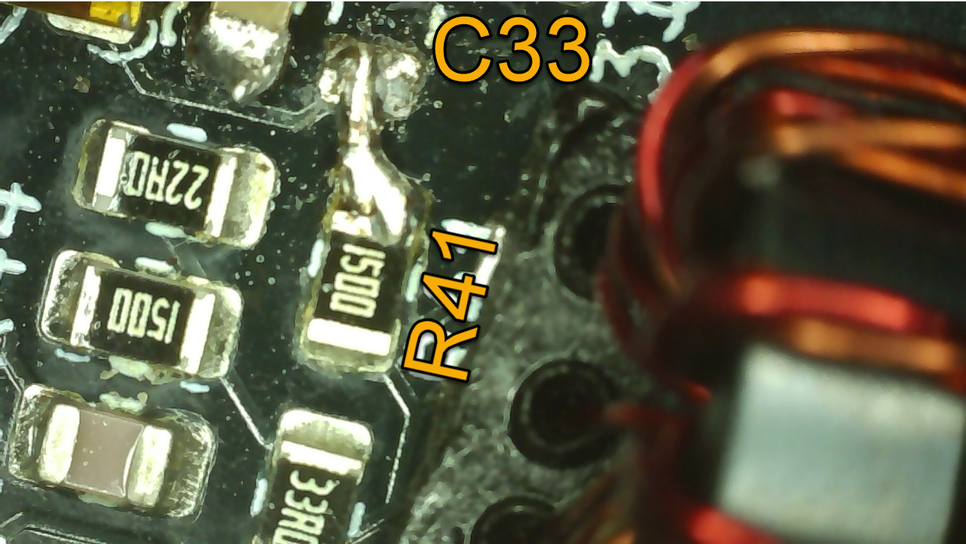
C33's second pad is now unused. Connect it to the nearest pad of R41 with a short wire or a solder bridge.
Keep this connection as short as possible. It provides an additional 1–2 dB of spur reduction.
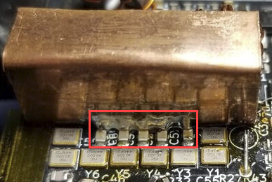
- Cut and bend a small U-shaped copper shield that will cover the three nearby coils (inductors) on the top and sides, like a small dog house.
- Cover the inside and outside of the shield with Kapton tape.
- Check the fit:
- The shield must not touch any component leads.
- Leave a small air gap above the components.
- The coils should be fully covered from the sides and top.
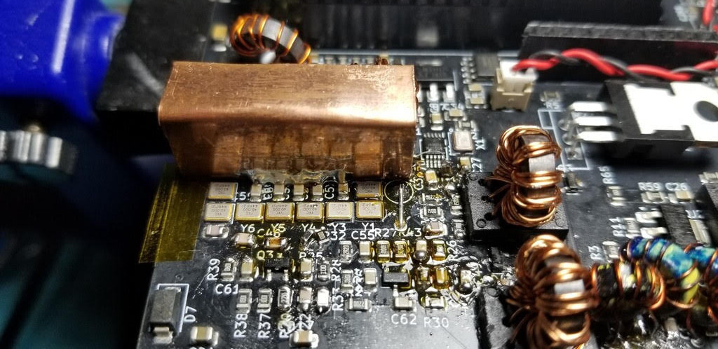
- Solder the shield to capacitors C52, C56, C58, C60, and C63 next to the coils. This grounds the shield and holds it in place.
- Do not solder to the crystal filters.
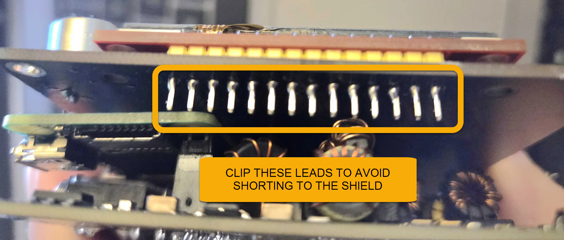
- Clip the display header leads so they cannot touch the shield.
- Look carefully for accidental solder bridges.
- Use a multimeter in continuity mode to confirm the shield is grounded (not floating) and that nothing is shorted.
After the mod, users typically see:
- Lower spur levels
- A cleaner transmitted spectrum
- Better performance at lower output power
- Less digital noise coupling
Results vary with build quality and layout tolerances.
This modification requires fine-pitch soldering and some RF experience. Perform it at your own risk. A poor job can degrade performance or damage the board. We are not responsible for any damage resulting from this mod. If you have doubts, then please seek a professional technician to perform the work for you.