TMS9918 Family
The TMS9918 is a Video Display Processor (VDP) designed by Texas Instruments, first released in 1979. It was used in a wide range of home computers and game consoles throughout the 1980s. The PICO9918 is a drop-in replacement for all variants in this family.
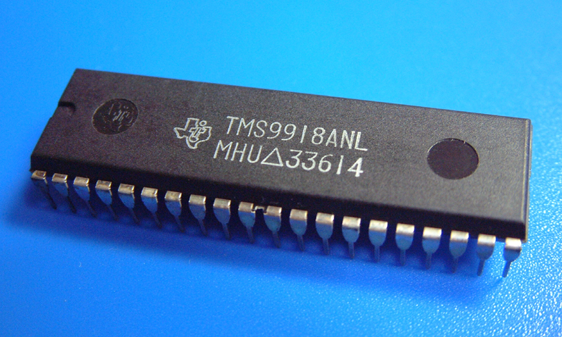
By Baz1521 at Japanese Wikipedia - Own work by the original uploader, CC BY-SA 3.0, Link
The TMS9918 family consists of several variants differing in video output, timing standard, DRAM interface, and feature support.
The model number encodes key characteristics:
-
First digit after TMS9:
9= original DRAM interface (8x 4164),1= revised DRAM interface (2x 4416) -
Second digit:
1= composite video output,2= component Y/R-Y/B-Y output -
Third digit:
8= 60 Hz (NTSC),9= 50 Hz (PAL) - Suffix A: The TMS9918A added Graphics II (bitmap) mode over the original TMS9918. All later variants (91xx) include GFX II regardless of suffix

-
Composite (
x1x8variants): Standard composite NTSC video. These chips also have a composite video input pin, allowing an external video signal to be overlaid. -
Y/R-Y/B-Y (
x2x8andx2x9variants): Component output providing separate luminance (Y) and colour difference (R-Y, B-Y) signals. These require an external encoder (e.g. MC1377) to generate composite or S-Video output. No video input pin.
The original TMS99xx series uses eight 16Kx1-bit DRAM chips (e.g. 4164) for 16 KB of VRAM. The function of one pin is changed on the later TMS91xx series, allowing two 16Kx4-bit DRAM chips (e.g. 4416) to be used instead. Both provide the same 16 KB of VRAM to the VDP.
The original TMS9918 (no 'A' suffix) lacks Graphics II mode (also known as bitmap mode). This mode allows a unique pattern and colour definition for every 8x1 pixel row on screen, enabling full bitmap graphics. All 'A' suffix and later variants support this mode.
The TMS9918A and TMS9928A/9929A provide two clock output signals derived from the VDP's crystal oscillator (10.738635 MHz for NTSC, 10.6875 MHz for PAL):
| Signal | Frequency | Purpose |
|---|---|---|
| GROMCLK | Crystal / 24 (~447 kHz) | Clocks GROM chips in TI-99 systems |
| CPUCLK | Crystal / 3 (~3.58 MHz) | Clocks the TMS9919 sound chip in TI-99 systems |
These signals are essential for TI-99 systems but unused by most other platforms (MSX, ColecoVision, SG-1000, etc.) which have independent clock sources.
Only the TMS9918 and TMS9918A provide both signals. The TMS9928A/9929A have GROMCLK but no CPUCLK. On the TMS91xx series, GROMCLK is not present — only CPUCLK remains (on pin 38 for the TMS9118, pin 37 for the TMS9128/9129).
The PICO9918 replaces all variants in this family. See Supported Devices for a full list of tested systems.
From firmware v1.1.1, the PICO9918 can be configured to match the GROMCLK / CPUCLK pin behaviour of the specific TMS9918 family variant it is replacing. This is set via the web-based configurator only — it is deliberately not exposed in the ROM-based configurator, so it cannot be accidentally changed from inside a working system. Set the device mode over USB before installing the PICO9918, then use the native configurator on the target machine for day-to-day settings.
| Device | Pin 37 | Pin 38 | Notes |
|---|---|---|---|
| TMS9918A | GROMCLK (~447 kHz) | CPUCLK (~3.58 MHz) | Default. |
| TMS992xA | GROMCLK (~447 kHz) | pulled low | CPUCLK output disabled. |
| TMS9118 | pulled low | CPUCLK (~3.58 MHz) | GROMCLK output disabled. |
| TMS912x | CPUCLK (~3.58 MHz) | pulled low | CPUCLK on pin 37 |
To pick the right mode, find your original VDP in the Chip Variants table above and match the GROMCLK / CPUCLK columns to the rows here.
If you need to fully disconnect either signal (e.g. when another source on the board drives the same net), use the CPU and GRM jumpers instead of — or in addition to — the device mode setting.