Repository navigation
Finish
The surface finish is the metal a fabricator deposits on the bare copper of a board: pads,
exposed traces, test points, the walls of the plated holes, the plated board edge and the
castellations. kese/s4_geometry/finish.py builds it on the faces and finish_shells.py on the
walls, in the holes and on the edge (shells.py lays each shell); the settings are in
parameters/finish.py.
Finish.FINISH_ENABLED = True: the finish adds its own thin solids on the copper, in every format
and both modes; it never changes the copper itself. False builds none, so the copper is bare as
KiCad draws it.
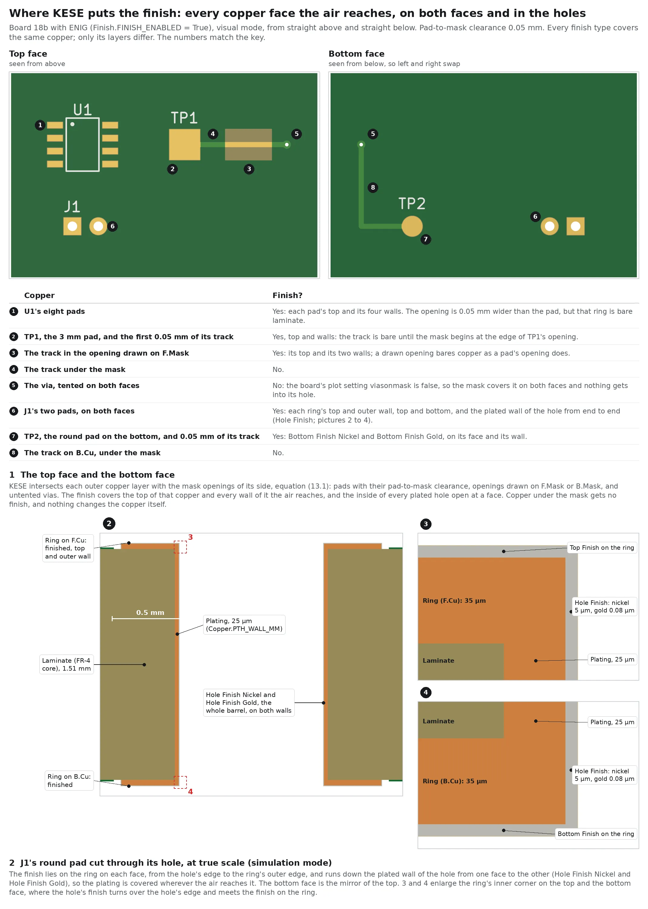
The finishes are deposited from baths (electroless nickel, immersion gold, silver and tin, OSP) or by dipping in solder (HASL), and both coat every copper face the liquid reaches, not only the faces seen from above. The solder mask goes on first and keeps the finish off the copper it covers ("solder mask over bare copper"; no finish deposits through the cured mask). So KESE puts the finish on every copper face the air reaches:
| Copper | Finish | Part |
|---|---|---|
| the top face of the outer copper in the mask openings (pads with their pad-to-mask clearance, drawn openings, untented vias) | stacked upward on the face, equation (13.2) |
Top Finish <metal>, Bottom Finish <metal>
|
| the side walls of that copper, where they meet the air: pads and traces in the openings, and the outer copper the board edge cuts | a shell beside the wall, equation (13.3), joined to the face's finish over the top corner | the same part as the face |
| the inner copper the board edge cuts (beside a castellation, say) | a shell beside the cut face, over the copper's height | Edge Finish <metal> |
| the plated board edge and the castellations' part-barrels (section 13.2.1) | a shell from the bottom of B.Cu to the top of F.Cu
|
Edge Finish <metal> |
| inside the bore of every plated hole open at a face | a shell over the barrel's whole length | Hole Finish <metal> |
Copper under the mask gets no finish, and a wall the mask touches none either. Neither does copper
under silkscreen ink kept in an opening (Silkscreen.SILKSCREEN_OVER_COPPER = True): the legend is
taken as printed before the finish. A hole closed at both faces gets no finish inside: a buried
hole, or a via tented on both faces (the mask closes it, so no liquid gets in); a via tented on one
face is finished from the other. On the face the finish layers are stacked from the top of the
outer copper outward, in the order the finish type lists them, each one its own solid:
On the B side every z is mirrored.
| Symbol | Meaning | Parameter |
|---|---|---|
finished face of side FINISH_GROUPING = "net") |
||
| outer copper of side |
||
| mask openings of side |
||
silkscreen ink of side SILKSCREEN_OVER_COPPER = True
|
Silkscreen.SILKSCREEN_OVER_COPPER |
|
| z range of finish layer |
||
| thickness of finish layer |
Finish.FINISH_TYPES |
|
|
|
laminate thickness and finished outer copper, equations (7.1) and (7.3) |
For ENIG on F.Cu of a board with no stack-up and (general (thickness 1.6)), so
Everywhere but the face, each finish metal is a shell in the air beside the copper Copper.EDGE_PLATING) or a castellation's part-barrel. The metals are
laid outward from the copper in the order the finish type lists them, as they are laid upward on
the face: with
where B.Cu to the top of F.Cu). Where the face next to
it takes the finish, it wraps over the corner: metal
A plated board edge is routed and plated before the finish goes on, so the finish covers the edge wall as it covers the pads; ENIG is the usual finish there, and an edge left under closed solder mask is plated but never finished (JLCPCB, PCB edge plating guide; Sierra Circuits, side plating). Castellations are plated holes cut through by the board edge; KESE finishes their part-barrels and their cut ends the same way.
Across a wall the shells are 2D shapes, so each metal is drawn a whole number of grid steps
(Geometry.SNAP_GRID_MM, 0.1 µm) thick, at least one: ENIG's 0.08 µm gold is drawn 0.1 µm thick
across a wall (its height on the face stays 0.08 µm). report.txt says so, for example
finish: also on the plated edge (Gold 8e-05 mm drawn 0.0001 mm thick across the edge, the snapping grid), and materials.json gives each shell part both thickness_mm and drawn_thickness_mm.
The finish is on by default, so every board of featureTest/ runs with it in the regression suite.
The air the shells fill, kese/s4_geometry/shells.py). The split is done in floating point, which keeps
every vertex, so two metals side by side share their edge vertex for vertex; only where two outlines
cross is the new vertex rounded onto the grid. Each piece is then noded on the grid as stage 6 nodes
every slice: where a metal one grid step thick comes out thinner than that between two slanted
edges (on a 45° wall a 0.1 µm band can come out 0.07 µm across, the spacing of 45° lines through
the grid points), noding closes it and leaves a hairline of air, so the prisms hold the volume the
solids will. Cutting the solid once, not once per metal, is what keeps the shells quick on a big
board; the copper layers and the hole spans are worked on Run.WORKERS at a time.
Finish.FINISH_BEFORE_SOLDER_MASK = False is the usual order above: mask first, finish after it.
With True the finish goes on first, as on a board electroplated with hard gold all over: all the
outer copper takes the finish, its faces (report.txt notes it on the finish: and solder mask: lines. Board 18c
(featureTest/18c_finish_before_mask.kicad_pcb, ENEPIG) runs with it on in the regression suite.
Finish.FINISH_TYPE is a key of the table below, "ENIG" by default, or "file" to take the type
from the stack-up's (copper_finish "..."). With "file" the name is compared, ignoring case,
spaces, - and _, with the keys of FINISH_TYPES and with the KiCad names in
Finish.FINISH_NAME_ALIASES. None means the board has no finish: nothing is built and
report.txt notes finish: the board's stackup says None, nothing applied. A board that names no
finish (no stack-up, or the field left empty), or a name that matches nothing, stops the run with
an error (FINISH ERROR: ... no finish was found in the KiCad file ...): change FINISH_TYPE or
set the finish in KiCad (Board Setup > Physical Stackup > Copper finish).
With KiCad's own finish names (the list in Board Setup's stack-up) this gives:
| KiCad finish | KESE type |
|---|---|
ENIG |
ENIG |
ENEPIG |
ENEPIG |
HAL SnPb |
HASL |
HAL lead-free |
HASL_LF |
Hard gold |
HardGold |
Immersion tin |
ImmersionTin |
Immersion silver |
ImmersionSilver |
OSP, HT_OSP
|
OSP |
None |
no finish |
Immersion nickel, Immersion gold, Not specified, User defined
|
no match: the run stops with an error (or add the name to FINISH_NAME_ALIASES) |
| Key | Layers, bottom to top (mm) |
|---|---|
ENIG |
Nickel 0.005, Gold 0.00008 |
ENEPIG |
Nickel 0.005, Palladium 0.0001, Gold 0.00005 |
HASL |
Tin 0.010 |
HASL_LF |
Tin 0.010 |
OSP |
OSP 0.0003 |
ImmersionSilver |
Silver 0.0002 |
ImmersionTin |
Tin 0.001 |
HardGold |
Nickel 0.005, Gold 0.001 |
The table is Finish.FINISH_TYPES and can be edited: add a key or change a thickness to match a
datasheet. report.txt names the type it applied and its layers, for example
finish: ENIG Nickel 0.005 mm + Gold 8e-05 mm. A FINISH_TYPE that is neither "file" nor a
key stops the run with an error.
Each finish below is shown on board 18b (featureTest/18b_finish_pads) with FINISH_ENABLED = True
and its key in FINISH_TYPE: 1 how it looks (visual mode), 2 a cut-away of the 3 mm pad TP1 at its
left edge (simulation mode), 3 the side profile at true scale with the height of every surface above
the laminate, and 4 the thin layers enlarged (HASL and HASL_LF need no part 4). Board 18b has 35 µm
copper on a 1.51 mm core, so its laminate face is at z = 0.755 mm and its copper top at 0.790 mm.
The bottom face is the mirror image, with the parts named Bottom Finish ....
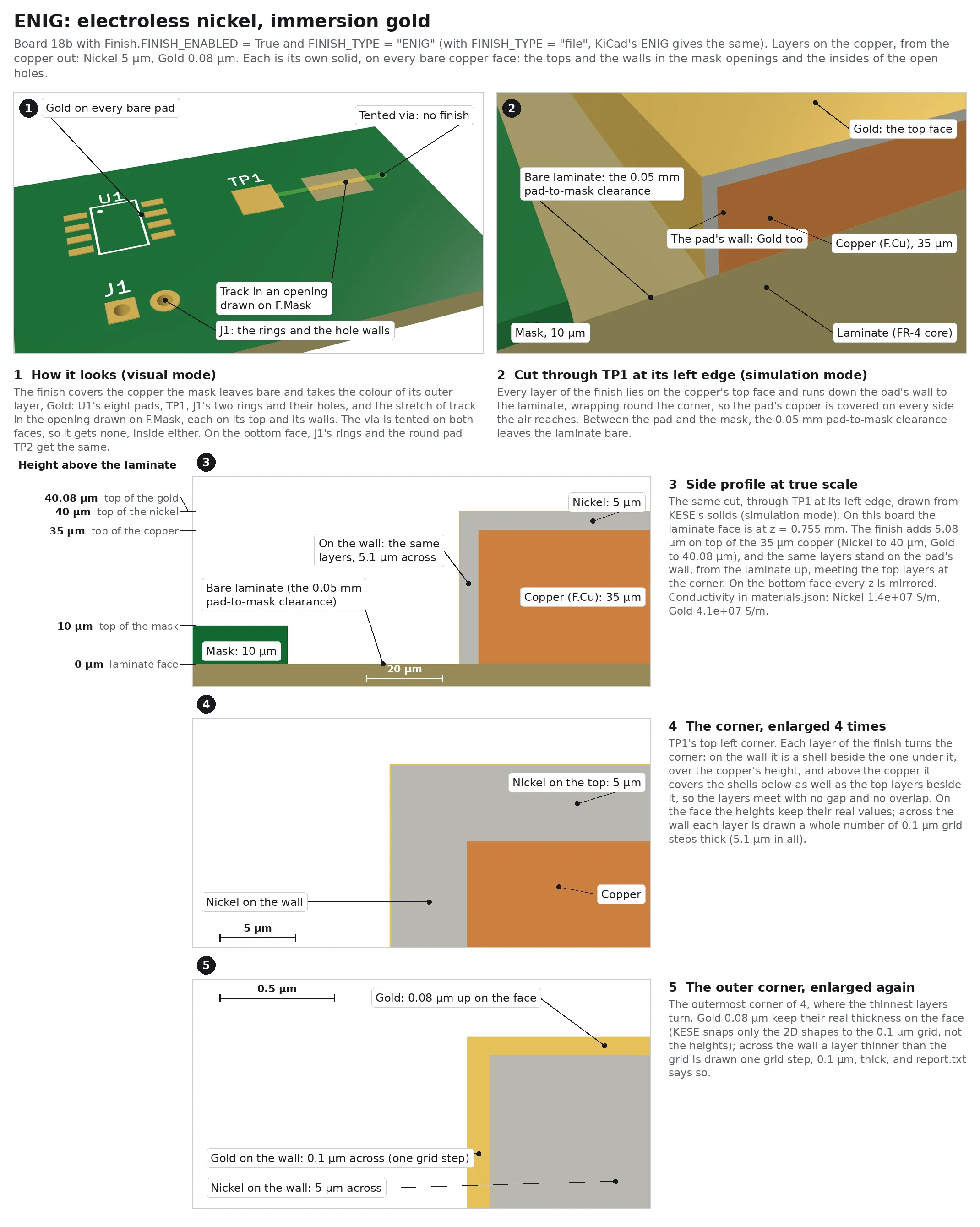
Electroless nickel, immersion gold; KiCad's ENIG.
| Layer, from the copper up | Thickness | Top above the copper | Part on the top face | Conductivity |
|---|---|---|---|---|
| Nickel | 5 µm | 5 µm | Top Finish Nickel |
1.4 × 10⁷ S/m |
| Gold | 0.08 µm | 5.08 µm | Top Finish Gold |
4.1 × 10⁷ S/m |
The pads take the gold's colour, #E6C15A. On board 18b the gold's top is 40.08 µm above the
laminate, at z = 0.79508 mm; at true scale the gold is under a pixel, so part 4 enlarges it.
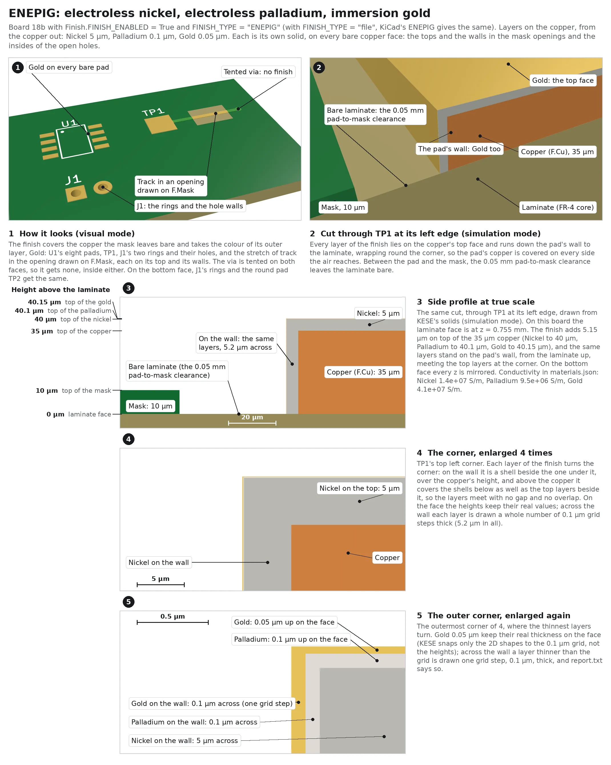
Electroless nickel, electroless palladium, immersion gold; KiCad's ENEPIG.
| Layer, from the copper up | Thickness | Top above the copper | Part on the top face | Conductivity |
|---|---|---|---|---|
| Nickel | 5 µm | 5 µm | Top Finish Nickel |
1.4 × 10⁷ S/m |
| Palladium | 0.1 µm | 5.1 µm | Top Finish Palladium |
9.5 × 10⁶ S/m |
| Gold | 0.05 µm | 5.15 µm | Top Finish Gold |
4.1 × 10⁷ S/m |
From the top it looks like ENIG (#E6C15A); the palladium shows only in a cut. On board 18b the
gold's top is 40.15 µm above the laminate.
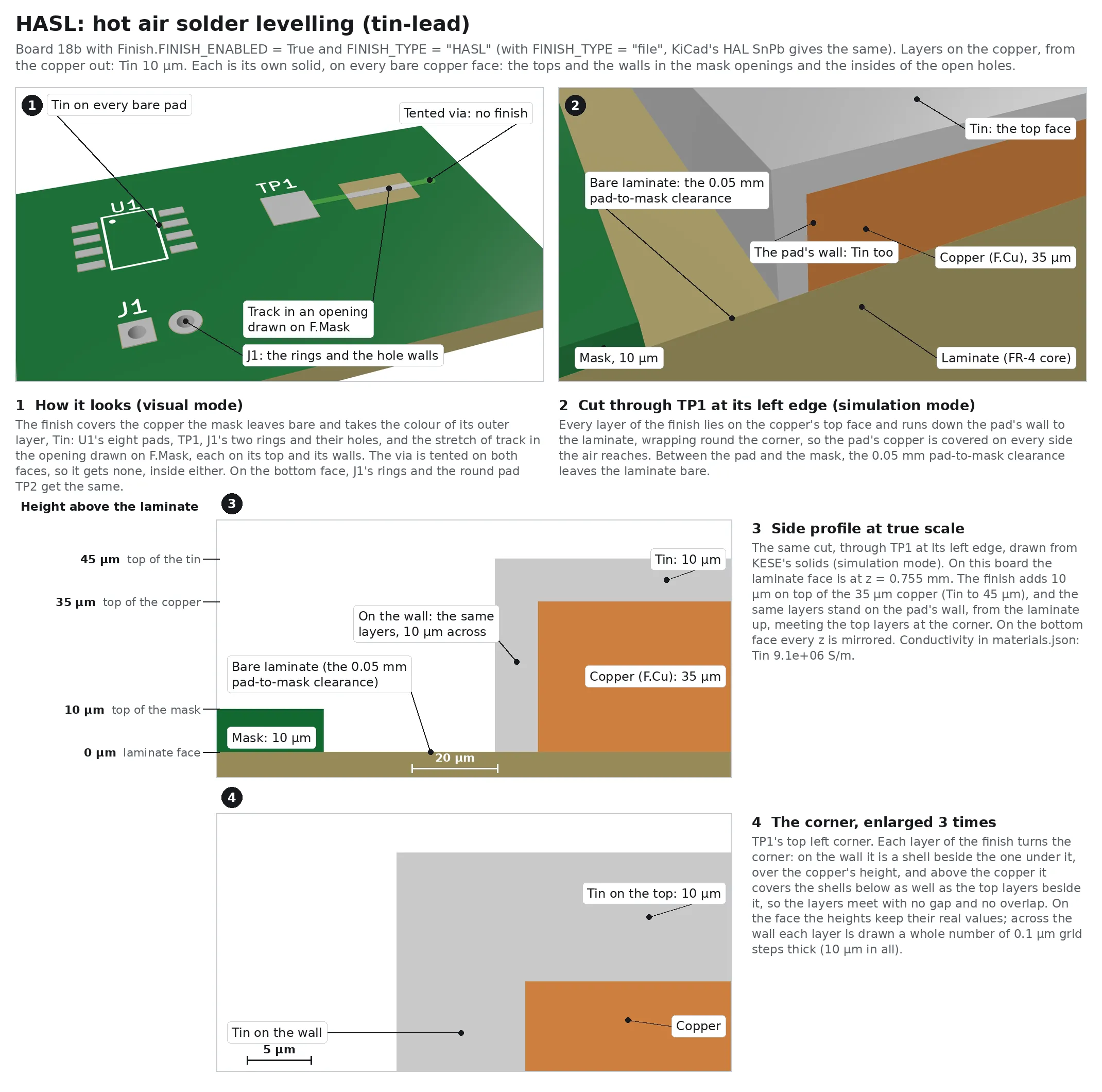
Hot air solder levelling with tin-lead solder; KiCad's HAL SnPb.
| Layer, from the copper up | Thickness | Top above the copper | Part on the top face | Conductivity |
|---|---|---|---|---|
| Tin | 10 µm | 10 µm | Top Finish Tin |
9.1 × 10⁶ S/m |
KESE models the solder as one flat layer of tin, coloured #C9C9C9. With HASL_LF it is the
thickest finish, and the only one with no layer thin enough to need part 4; on board 18b its top is
45 µm above the laminate.
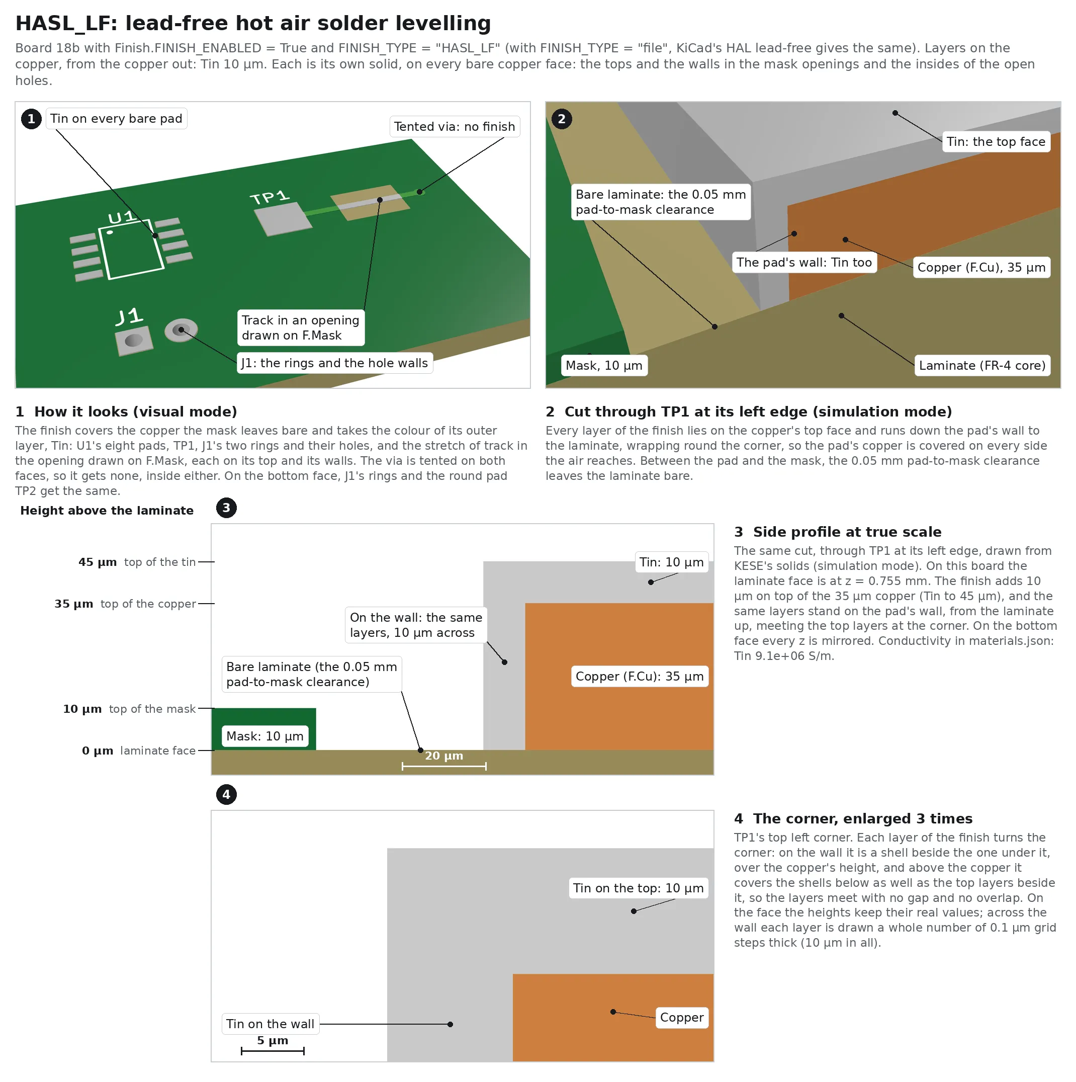
Lead-free hot air solder levelling; KiCad's HAL lead-free.
| Layer, from the copper up | Thickness | Top above the copper | Part on the top face | Conductivity |
|---|---|---|---|---|
| Tin | 10 µm | 10 µm | Top Finish Tin |
9.1 × 10⁶ S/m |
KESE builds it exactly as HASL: the same layer of tin, the same part and the same colour.
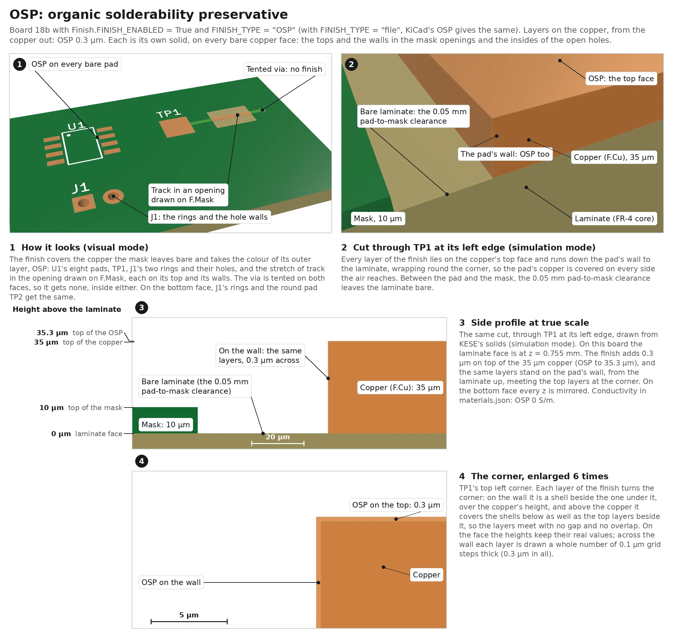
Organic solderability preservative; KiCad's OSP and HT_OSP.
| Layer, from the copper up | Thickness | Top above the copper | Part on the top face | Conductivity |
|---|---|---|---|---|
| OSP | 0.3 µm | 0.3 µm | Top Finish OSP |
0 (organic) |
Coloured #D9955A, close to the copper under it. On board 18b its top is 35.3 µm above the
laminate.
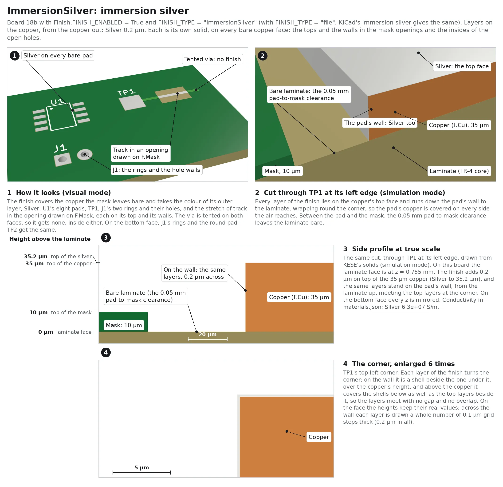
Immersion silver; KiCad's Immersion silver.
| Layer, from the copper up | Thickness | Top above the copper | Part on the top face | Conductivity |
|---|---|---|---|---|
| Silver | 0.2 µm | 0.2 µm | Top Finish Silver |
6.3 × 10⁷ S/m |
Coloured #E4E4E0. On board 18b its top is 35.2 µm above the laminate.
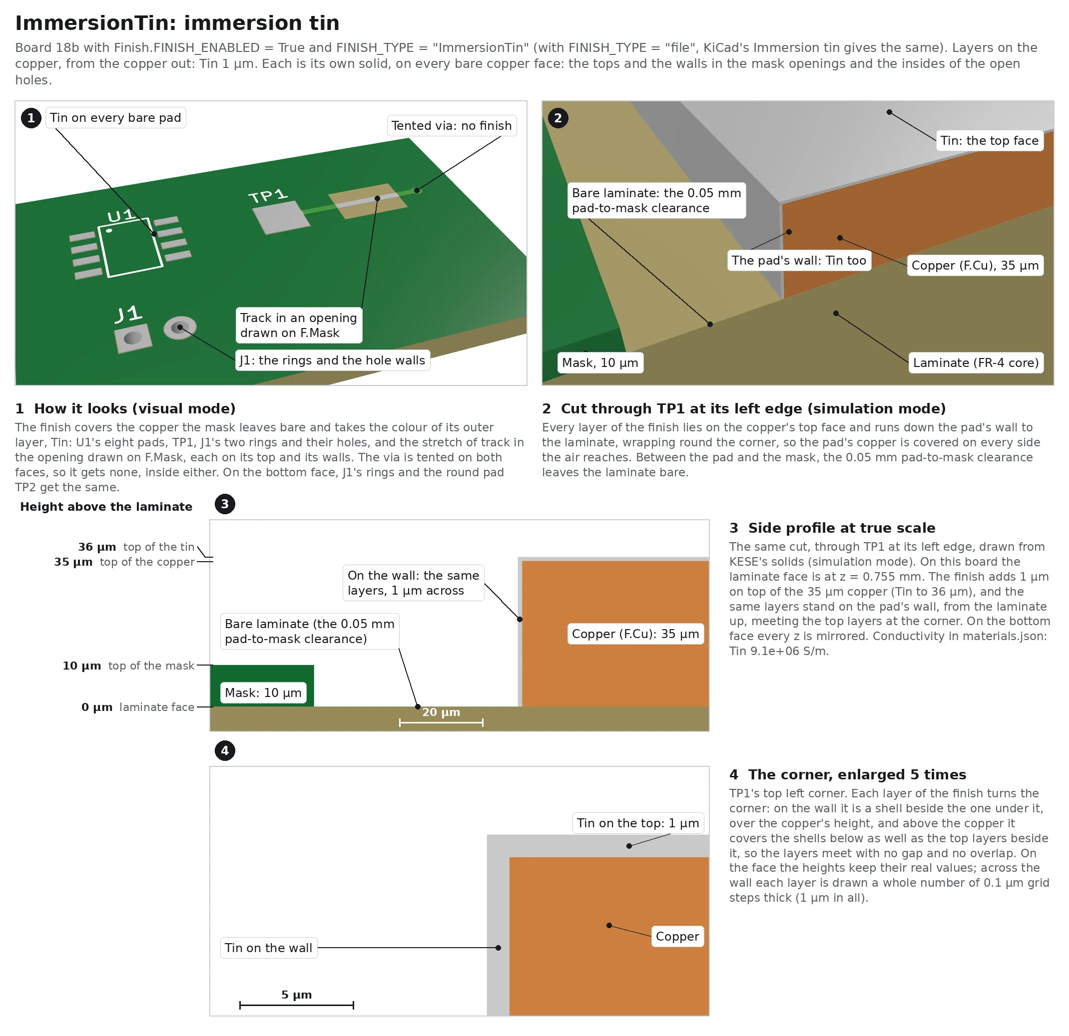
Immersion tin; KiCad's Immersion tin.
| Layer, from the copper up | Thickness | Top above the copper | Part on the top face | Conductivity |
|---|---|---|---|---|
| Tin | 1 µm | 1 µm | Top Finish Tin |
9.1 × 10⁶ S/m |
The metal of HASL, a tenth as thick, with the same part name and colour (#C9C9C9). On board 18b
its top is 36 µm above the laminate.
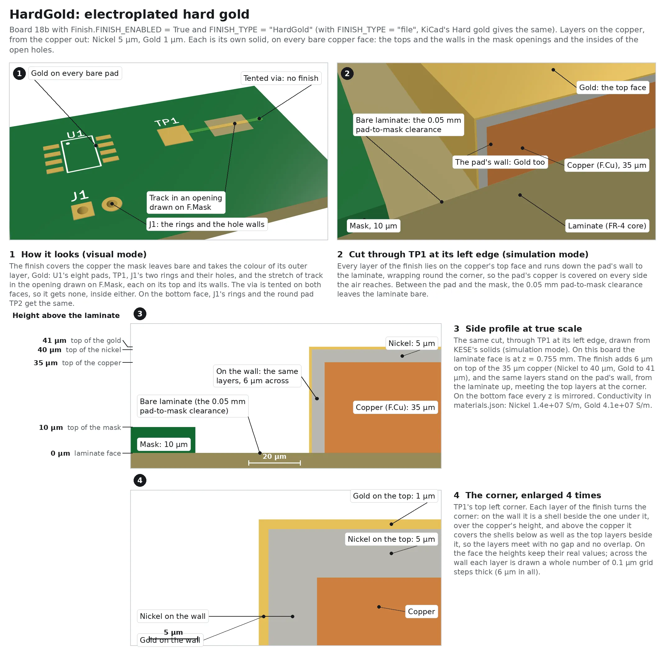
Electroplated hard gold, the finish of edge-connector fingers; KiCad's Hard gold.
| Layer, from the copper up | Thickness | Top above the copper | Part on the top face | Conductivity |
|---|---|---|---|---|
| Nickel | 5 µm | 5 µm | Top Finish Nickel |
1.4 × 10⁷ S/m |
| Gold | 1 µm | 6 µm | Top Finish Gold |
4.1 × 10⁷ S/m |
The thickest gold of the eight finishes, 12.5 times ENIG's; the pads look gold (#E6C15A). On
board 18b the gold's top is 41 µm above the laminate.
Finish.FINISH_GROUPING:
| Value | Parts | Example |
|---|---|---|
"metal" (default) |
one per side and metal |
Top Finish Nickel, Top Finish Gold, Bottom Finish Nickel, Edge Finish Nickel, Hole Finish Gold, ... |
"net" |
one per side, metal and net |
Top Finish Gold_GND, so a net's copper, nickel and gold can be picked together in the solver (Copper_GND, Top Finish Nickel_GND, Top Finish Gold_GND, Edge Finish Gold_GND, Hole Finish Gold_GND) |
In materials.json each finish part has the layer F.Finish, B.Finish, Edge.Finish or
Hole.Finish, its z_range_mm, and the properties side (F, B, Edge or Hole), metal,
thickness_mm and conductivity_S_per_m, and on the shells drawn_thickness_mm (section 13.2.1); the conductivities come
from Finish.FINISH_CONDUCTIVITY_S_PER_M (Nickel 1.4 × 10⁷, Gold 4.1 × 10⁷, Palladium 9.5 × 10⁶,
Tin 9.1 × 10⁶, Silver 6.3 × 10⁷ S/m, OSP 0 since it is organic). Colours come from the metal's entry
in Color.MATERIALS (Colorizing).
In STEP, finish parts are written as every other part, each as the closed solids stage 6 built, one per connected piece.
Note
The gold of ENIG is 80 nm thick and that of ENEPIG 50 nm. Heights are not snapped to the
0.1 µm grid (only the 2D shapes are), so in simulation mode each is built as a real solid, but
an FDTD or FEM mesher may not resolve a body that thin. Solvers that struggle can take the finish
as a surface impedance instead and leave FINISH_ENABLED off. In visual mode only the surface
between material and air is kept (Output Modes): the faces where two layers
touch are dropped, so a pad's top and walls show the outermost layer alone, and the layers under
it show only where a cut opens them.
| Name | Default | Range | Meaning |
|---|---|---|---|
FINISH_ENABLED |
True |
bool | Build the finish and write it to every file |
FINISH_TYPE |
"ENIG" |
"file" or a key of FINISH_TYPES
|
The type, or "file" for the stack-up's (an error when the file names none) |
FINISH_GROUPING |
"metal" |
"metal" / "net"
|
Part per metal, or per metal and net |
FINISH_BEFORE_SOLDER_MASK |
False |
bool | Finish on all the outer copper, under the mask (section 13.2.2), instead of only where the mask leaves it bare |
FINISH_TYPES |
table above | {key: [(metal, mm), ...]} |
Layers of each finish |
FINISH_NAME_ALIASES |
HAL SnPb → HASL, HAL lead-free → HASL_LF, Hard gold → HardGold, Immersion tin → ImmersionTin, Immersion silver → ImmersionSilver, HT_OSP → OSP
|
{KiCad name: key} |
KiCad's finish names that differ from a key |
FINISH_CONDUCTIVITY_S_PER_M |
table above | {metal: S/m} |
Written to materials.json
|
| Previous | Next |
|---|---|
| Colorizing | Silkscreens |