Structure and Grains
Beyond the spectroscopy and diffraction tools, FermiViewer has two workshops for microstructure: grain segmentation and cross-section layer analysis. Both open from the Analysis / Window menus and act on the active image.
The grain workshop segments a micrograph into grains and reports the statistics materials scientists actually quote.
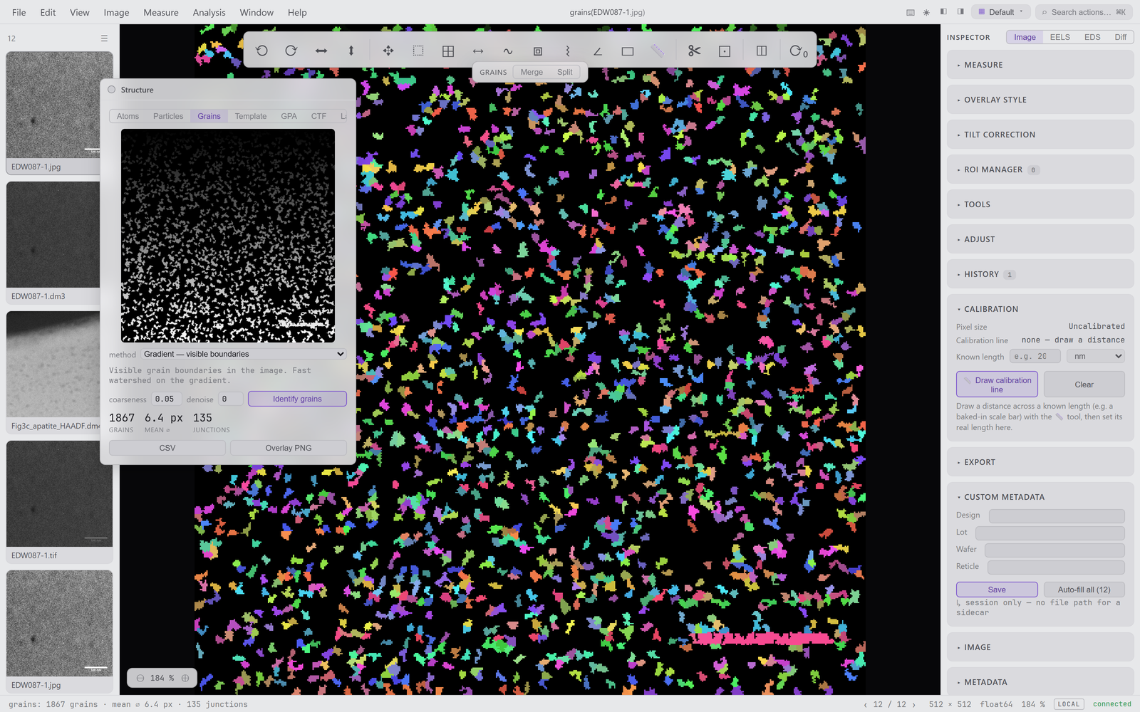
Pick a method from the dropdown — each explains when to reach for it, right under the picker:
- Gradient — visible boundaries — a fast watershed on the image gradient. Best when the grain boundaries are actually visible.
- k-means intensity — clusters by grey level; best for phase contrast where grains differ in brightness. This is the method verified against the MATLAB reference.
- SLIC + region merging — superpixels merged by similarity; good for textured grains without crisp boundaries.
- Orientation (structure tensor) — segments by local lattice orientation, for lattice-resolved images.
Tune coarseness (and the optional denoise knob) and click Identify grains. The metric tiles summarize the result at a glance — grain count, mean diameter, and triple-junction count, plus an ASTM grain-size number when the image carries a calibration. Export the labelled map as an Overlay PNG or the per-grain table as CSV.
A grain map opens a Merge / Split editor on the stage:
- Merge — click two adjacent grains to fuse them.
- Split — click one grain to re-segment it with a finer watershed.
The statistics recompute after each edit.
Some grains the automatic methods miss. The Trained — paint examples method teaches a random-forest pixel classifier by example:
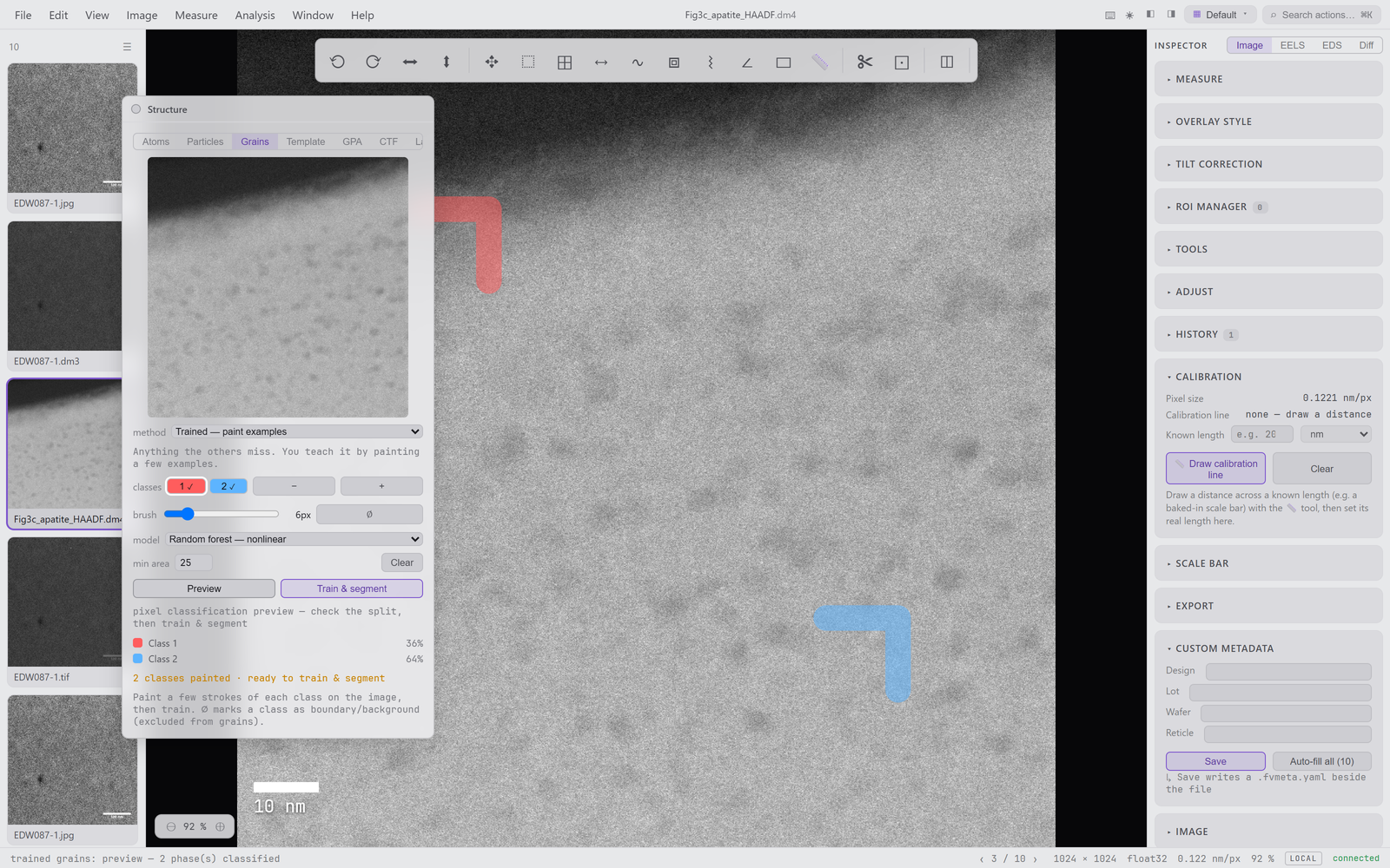
- Choose Trained — paint examples and pick a class (add as many as you need; the ∅ button marks a class as boundary/background, excluded from grains).
- Paint a few strokes of each class on the image — the ✓ chips light up as each class gets examples, and a hint tells you when you're ready.
- Click Preview to see the predicted pixel-class split before committing. Adjust your strokes and preview again until it looks right.
- Train & segment turns the classified phases into a grain map you can edit like any other.
The model dropdown selects the classifier (random forest by default); min area drops specks below the given pixel count.
The Cross-section Layers workshop measures a thin-film stack in cross-section: it finds the layers, measures each layer's average thickness across the field of view, and quantifies the interface roughness two ways.
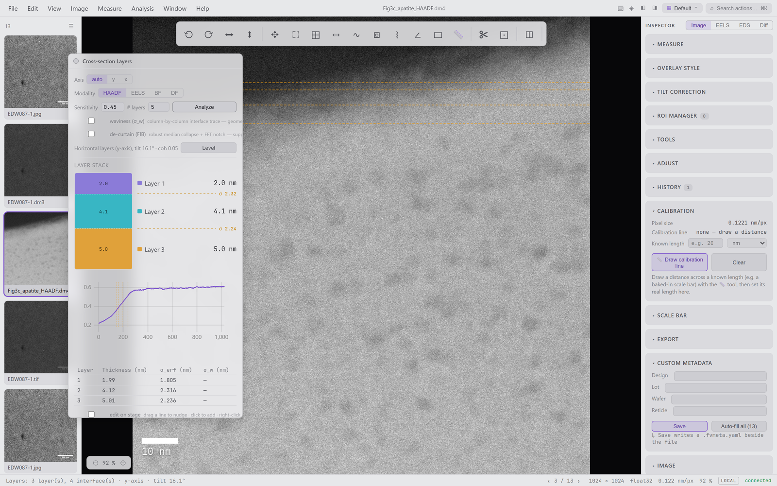
- Layer stack — a band diagram where each detected film is sized by its thickness, with dashed σ_erf rails showing how sharp each interface is. The thickness table reads out in nm when the image is calibrated, otherwise in pixels.
- Growth axis — auto-detected (or force x / y); the workshop reports the detected tilt and coherence.
- Modality — HAADF, EELS, or BF/DF. BF/DF use scale-space detection to reject thickness fringes.
- Sensitivity and an optional # layers hint control how many interfaces survive.
- Roughness — tick waviness (σ_w) to trace each interface column-by-column. σ_w is measured rigorously — far beyond a point-to-point cursor measurement: the trace is detrended (tilt and substrate bow removed), outlier columns are rejected (with a "% columns OK" quality flag), the shot-noise edge-localisation jitter is estimated and subtracted in quadrature, and a block-bootstrap 95% confidence interval accompanies every value in the table.
- de-curtain (FIB) — a robust median collapse + FFT notch that suppresses FIB curtaining artifacts before analysis.
- Level rotates the image so the layers sit horizontal; edit on stage lets you drag, add, or remove interfaces, and the fit recomputes.
Click an interface number under the table — or click its dashed line on the image — for the full roughness report:
- σ_w ± CI with the raw σ and noise floor it was derived from.
- Correlation length ξ and Hurst exponent H from a self-affine height–height-correlation fit — the same roughness language as XRR/AFM analysis.
- σ_chem — the intrinsic (chemical) transition width, decomposed as √(σ_erf² − σ_w²): the erf width of the laterally averaged profile convolves real compositional grading with geometric waviness, and this removes the waviness part.
-
Roughness spectrum — a log–log PSD of the interface trace. Enter an
approximate foil thickness (
≈ foil t) and the projection-limited region is shaded: a TEM cross-section averages through the foil, so roughness at lateral wavelengths shorter than the foil is invisible and σ_w reads as a lower bound. - conf r (in the table) — the correlation between a layer's two interface traces: r ≈ 1 means the top interface replicates the bottom one (conformal growth); r ≈ 0 means the roughness is independent.
The theory (formulas, references) is documented in the repo under
docs/theory/interface-roughness.md.
Export the per-layer + per-interface table (thickness, σ_erf, σ_w ± CI, quality, ξ, H, σ_chem) as CSV.
Next: AFM Support.