wiring jtag debug
Understand the four core JTAG signals and their direction at a target.
Applies to: Single-target signal diagram. Pin order, voltage and optional reset signals depend on the exact probe and connector.
Using supported programming, debugging or boundary-scan tools with documented target hardware.
Separate clock, state control and serial input/output let a probe communicate with a target's test-access port.
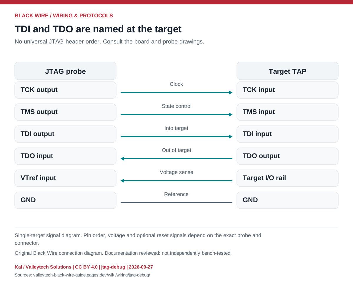
| Target signal | Direction at target | Purpose |
|---|---|---|
| TCK | Input | Clock |
| TMS | Input | State selection |
| TDI | Input | Serial data in |
| TDO | Output | Serial data out |
- Match the target connector and I/O voltage; identify optional nTRST and system reset separately.
- For multiple targets, use the documented chain order and instruction-register configuration.
- Do not assume that a similarly sized header is JTAG.
- Do not connect a probe's power-output contact unless the board and probe documentation explicitly allow it.
This is a general interface guide; match your own hardware documentation.
Source documents inspected; independent electrical and bench review pending. Reviewed 2026-09-27.
- SEGGER: J-Link interface description — 20-pin JTAG signal direction and VTref; checked 2026-09-27
Original writing and diagram by Kal / Valleytech Solutions, CC BY 4.0. Manufacturer artwork and documentation retain their own rights.
CC BY 4.0 · SHA-256: b5c8e670c2135bf8572589c08071c3c57c0e6f84a06b08efd8ae43f413888f80