P3X OFDM Receiver board
Function
Variants
Parts
Programming
External interfaces
Service interfaces
Board view
Schematics
The OFDM Receiver module is responsible for pairing with RC and communicating with it. The name comes from Orthogonal Frequency Division Multiplexing - which is a way of transferring broadband data. It implements the Lightbridge technology, and is also a middleman between the gimbal and flight controller.
The Lightbridge transmission system is based on WiMAX, but uses custom processing of digital signals.
There are multiple versions of the board, with two major lines. The older OFDM boards implement Lightbridge via Altera FPGA chip, while later boards use Artosyn Custom Radio chips. Switching from multi-purpose chips to dedicated ASICs reduced cost and power consumption of the boards. The Custom Chip manufactured by Artosyn has a design which exactly matches the previously used FPGA bitstream, so both boards are compatible with GL300a/b/c Radio Controllers.
| Marking | Overview |
|---|---|
| P01007.06 | First known version. |
| P01007.08 | Switched to different voltage regulators. |
| P01007.14 | Switched from FPGA to Custom Chip; often called OFDM v2 module. |
Full list of known components is presented in the table.
| Marking | Amt. | Pkg. | Function | Specification |
|---|---|---|---|---|
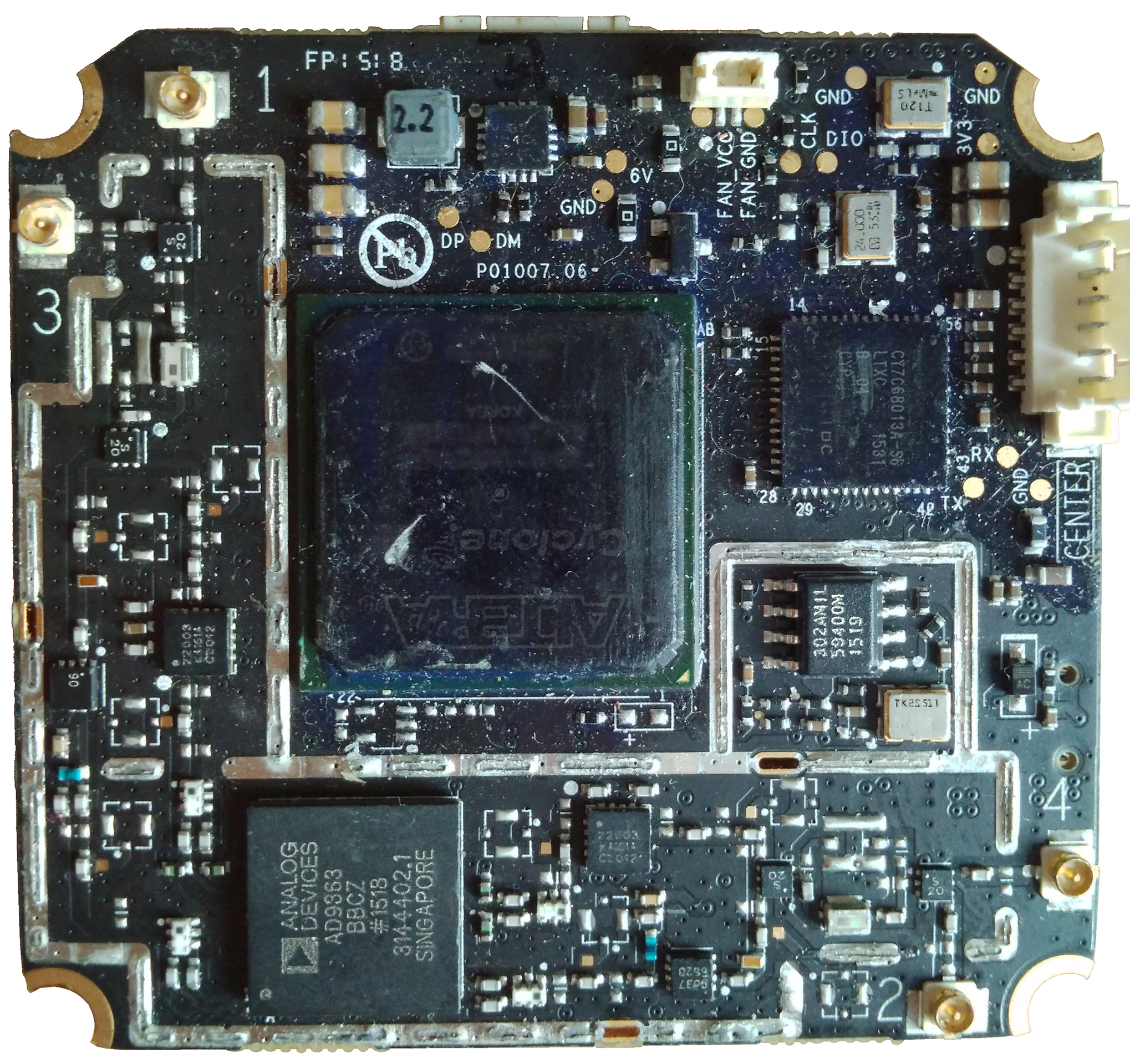
| STM32F 103CBU6 GH24W 93 CHN 516 | 1 | 48-lead 7x7 UFQFPN | Mainstream Performance line, ARM Cortex-M3 MCU with 128Kbytes Flash, 72MHz CPU, motor control, USB and CAN; Lightbridge MCU | description |
| ATH520 64DM Y | 1 | 8-pin | SPI Serial EPPROM integrated chip; FPGA bitstream storage | |
| 25Q064A 13E40 60 CHN 51712S | 1 | 8-pin 4x5 SOP | Micron Serial NOR Flash Memory; 64Mb, 1.8V, Multiple I/O, 4KB Sector Erase | datasheet |
| AEKF | 1 | 8-pin SOT23 | Maxim MAX3051EKA+T 1Mbps, Low-Supply-Current CAN Transceiver | datasheet |
| PA 5QA | 1 | 3x3 UDFN/WSON | Mini Linear Regultor; part used is DI AP7361ADJ, but it could also be TI TPS7A16 | DI datasheet TI description |
| 1755 ADJ #518 0220 | 1 | 16-lead 4x4 LFCSP-WQ | 1.2A Low-Vin, Adjustable-Vout LDO Linear Regulator | description |
| AD9363 BBCZ #1518 3144402.1 Singapore | 1 | 144-ball 10x10 CSP-BGA | Analog Devices Agile Radio frequency (RF) 2x2 transceiver with integrated 12-bit DACs and ADCs; Lightbridge RF transceiver | description |
| VUBI TI 54 SI8F | 3 | 16-pin 3x3 QFN-4444 | Texas Instruments TLV62130RGTR 3V to 17V 3A Step-Down Converter | description |
| 22003 KA1614 CL012 | 2 | 16-lead 3x3 QFN | Avago MGA-22003 2.3-2.7GHz WiMAX and WiFi Power Amplifier | description |
| 9037 6620 | 2 | 8-lead 2x2 QFN-44 | TriQuint TQP3M9037 Ultra Low Noise, High Linearity LNA | datasheet |
| S 20 | 4 | 6-lead 1.5x1.5 QFN-33 | SKY13320-374LF: 0.1-6.0GHz GaAs SPDT Switch | description |
| 302AMIL 59400M 1519 | 1 | |||
| AC | 1 | diode? | ||
| TK2S 519 | 1 | Quartz oscillator? | ||
| T120 MeLS | 1 | Quartz oscillator, 12MHz | ||
| 24.000 53 Rite | 1 | Quartz oscillator, 24MHz | ||
| Altera Cyclone V 5CEFA4U19I7 | 1 | 484-ball UFBGA | FPGA; Cyclone V E model 5CEA4, temp. range -40 to 100degC; Lightbridge digital data scrambler; handles input and output data streams of the RF transceiver | description |
| CY7C68013A-56 LTXC 1531 B 04 CYP squareC | 1 | 56-lead 8x8 QFN | EZ-USB FX2LP USB Microcontroller High-Speed USB Peripheral Controller; Lightbridge deserializer; receives H.264 encoded video data stream from USB input and deserializes it for Lightbridge digital data scrambler | description |
The part list is almost identical to P01007.08. The changes are TLV62130RGTR regulators which have been replaced. Only new components will be provided in the table.
| Marking | Amt. | Pkg. | Function | Specification |
|---|---|---|---|---|
| IAEU6 | 2 | Step-Down Converter |
Full list of known components is presented in the table.
| Marking | Amt. | Pkg. | Function | Specification |
|---|---|---|---|---|
| STM32F 103CBU6 GH24W 93 CHN 536 | 1 | Mainstream Performance line, ARM Cortex-M3 MCU with 128Kbytes Flash, 72MHz CPU, motor control, USB and CAN; Lightbridge MCU | description | |
| ATH542 64DM Y A3GXAA | 1 | 8-pin | SPI Serial EPPROM integrated chip; FPGA bitstream storage | |
| AEKF | 1 | 8-pin SOT23 | MAX3051EKA+T 1Mbps, Low-Supply-Current CAN Transceiver | datasheet |
| K7K CN | 1 | |||
| PA 6DA | 1 | Step-Down Converter? | ||
| Xlat 20.000 605E | 1 | quartz oscillator, 20MHz | ||
| M9Y9975 46.5.8 | 1 | quartz oscillator? | ||
| S 20 | 4 | SKY13320-374LF: 0.1-6.0GHz GaAs SPDT Switch | description | |
| Xlat 24.000 68 | 1 | quartz oscillator, 24MHz | ||
| Xlat T120 Px25 | 1 | quartz oscillator, 12MHz | ||
| IAEU6 | 2 | Step-Down Converter | ||
| 53 625 | 1 | |||
| VS6 U | 1 | |||
| CY7C68013A-56 LTXC 1531 B 04 TWN CYP 626064 squareC | 1 | EZ-USB FX2LP USB Microcontroller High-Speed USB Peripheral Controller; Lightbridge deserializer; receives H.264 encoded video data stream from USB input and deserializes it for Lightbridge digital data scrambler | description | |
| PA 5206 WNSA | 2 | |||
| Artosyn AR8003 CAK841 1603 | 1 | Lightbridge RF transceiver; WiMAX 2T2R, frequencies 2.3G-2.6G or 3.3G-3.8G, modulations BPSK, QPSK, 16QAM, 64QAM adaptive | ||
| Artosyn AR8001 612P6042 | 1 | Lightbridge digital data encoder/scrambler; handles input and output data streams of the RF transceiver, implements digital processing previously handled by FPGA Bitstream |
| Chips | Firmware | Description |
|---|---|---|
| cy7c68013a | m1500 | Provides communication with camera module, including video transmission. |
| Altera Cyclone 5 E + ATH542 | m1900 | Lightbridge FPGA air part; NAND flash memory stores the programming and the FPGA chip reads it during each startup. |
| STM32F103 | m0900 | Lightbridge MCU; configures and drives FPGA and transceiver. |
Connectors on the board are:
| Marking | Overview |
|---|---|
| CAMERA 6-pin 1.25mm ribbon cable con. | ribbon cable to the Gimbal top board |
| CENTER 6-pin ribbon cable con. | ribbon cable to the ESC center board |
The following service pads exist on this board:
| Marking | Overview |
|---|---|
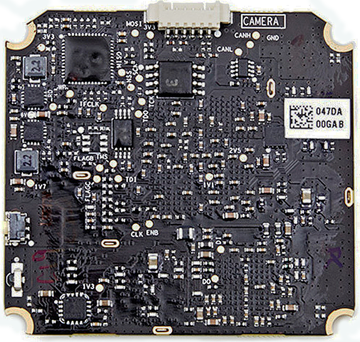
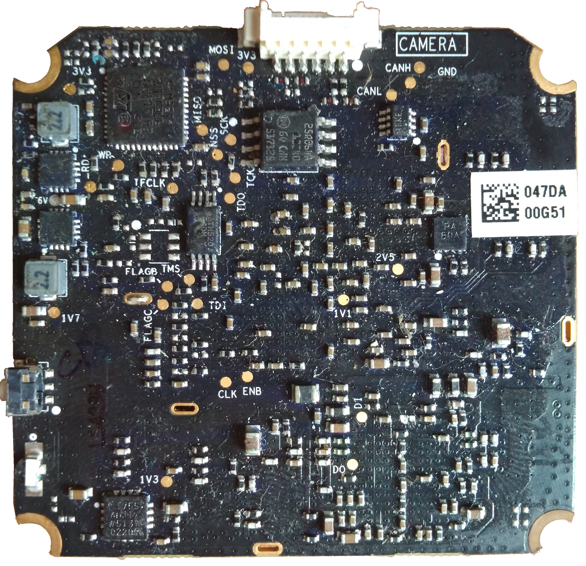
| DP | CAMERA con. USB-DP; top side |
| DM | CAMERA con. USB-DM; top side |
| GND | CENTER con. ground; top side |
| 6V | CENTER con. power; top side |
| FAN_VCC | Cooling fan con.; top side |
| FAN_GND | Cooling fan con.; top side |
| GND | Ground; top side |
| CLK | Serial Wire Debug clock; top side |
| DIO | Serial Wire Debug i/o; top side |
| 3V3 | Regulated 3.3V power supply; top side |
| GND | Ground; top side |
| TX | CENTER con. FC serial transmit; UART 256000 8n1; top side |
| RX | CENTER con. FC serial receive; UART 256000 8n1; top side |
| GND | CENTER con. ground; top side |
| 6V | CENTER con. power; bottom side |
| RD | Cypress Slave FIFO mode read; bottom side |
| WR | Cypress Slave FIFO mode write; bottom side |
| IFCLK | Cypress IfClk; bottom side |
| 3V3 | Regulated 3.3V power; bottom side |
| MOSI | SPI Master Output Slave Input line; bottom side |
| MISO | SPI Master Input Slave Output line; bottom side |
| 3V3 | Regulated 3.3V power; marking behind connector; bottom side |
| NSS | SPI Slave Select line; bottom side |
| SCK | SPI Clock line; bottom side |
| TDO | JTAG Test Data Out; bottom side |
| TCK | JTAG Test Clock; bottom side |
| CANL | CAN bus Lo line; bottom side |
| CANH | CAN bus Hi line; bottom side |
| GND | Ground; bottom side |
| 2V5 | Regulated 2.5V power; bottom side |
| 1V1 | Regulated 1.1V power; bottom side |
| DI | unknown data in; bottom side |
| DO | unknown data out; bottom side |
| 1V3 | Regulated 1.3V power; bottom side |
| CLK | unknown clock; bottom side |
| ENB | unknown enable; bottom side |
| 1V7 | Regulated 1.7V power; bottom side |
| TDI | JTAG Test Data In; bottom side |
| TMS | JTAG Test Mode Select; bottom side |
| FLAGB | Cypress FlagB line; bottom side |
| FLAGC | Cypress FlagC line; bottom side |
The following service pads exist on this board:
| Marking | Overview |
|---|---|
| 5V | CENTER con. power; top side |
| GND | CENTER con. ground; top side |
| DP | CAMERA con. USB-DP; top side |
| DM | CAMERA con. USB-DM; top side |
| FAN_VCC | Cooling fan con.; top side |
| FAN_GND | Cooling fan con.; top side |
| SWCLK | Serial Wire debug clock; top side |
| SWDIO | Serial Wire debug i/o; top side |
| GND | Ground; top side |
| 5V | CENTER con. power; top side |
| RX | CENTER con. FC serial receive; UART 256000 8n1; top side |
| TX | CENTER con. FC serial transmit; UART 256000 8n1; top side |
| GND | Ground; top side |
| MOSI | SPI Master Output Slave Input line; bottom side |
| MISO | SPI Master Input Slave Output line; bottom side |
| 3V3 | Regulated 3.3V power; marking behind connector |
| CANL2 | CAN bus Lo line; bottom side |
| CANH2 | CAN bus Hi line; bottom side |
| GND | Ground; bottom side |
| SCK | SPI Clock line; bottom side |
| NSS | SPI Slave Select line; bottom side |
| 3V3_MCU | Power; bottom side |
| 5V | Power; bottom side |
| VDDA33_VCO1 | ; bottom side |
| IFCLK | Cypress IfClk; bottom side |
| SLRD# | Cypress Slave FIFO mode read; bottom side |
| SLWR# | Cypress Slave FIFO mode write; bottom side |
| FLAGC# | Cypress FlagC line; bottom side |
| FLAGB# | Cypress FlagB line; bottom side |
| RX1 | UART serial interface 1 receive; bottom side |
| TX1 | UART serial interface 1 transmit; bottom side |
| RX2 | UART serial interface 2 receive; bottom side |
| TX2 | UART serial interface 2 transmit; bottom side |
| GND | Ground; bottom side |
| 1V2 | Regulated 1.2V power; bottom side |
| 1V8 | Regulated 1.8V power; bottom side |
| VCCMCU_3V3 | Regulated 3.3V power; bottom side |
| CLK | unknown clock; bottom side |
| ENB | unknown enable; bottom side |
| DO | unknown data out; bottom side |
| DI | unknown data in; bottom side |
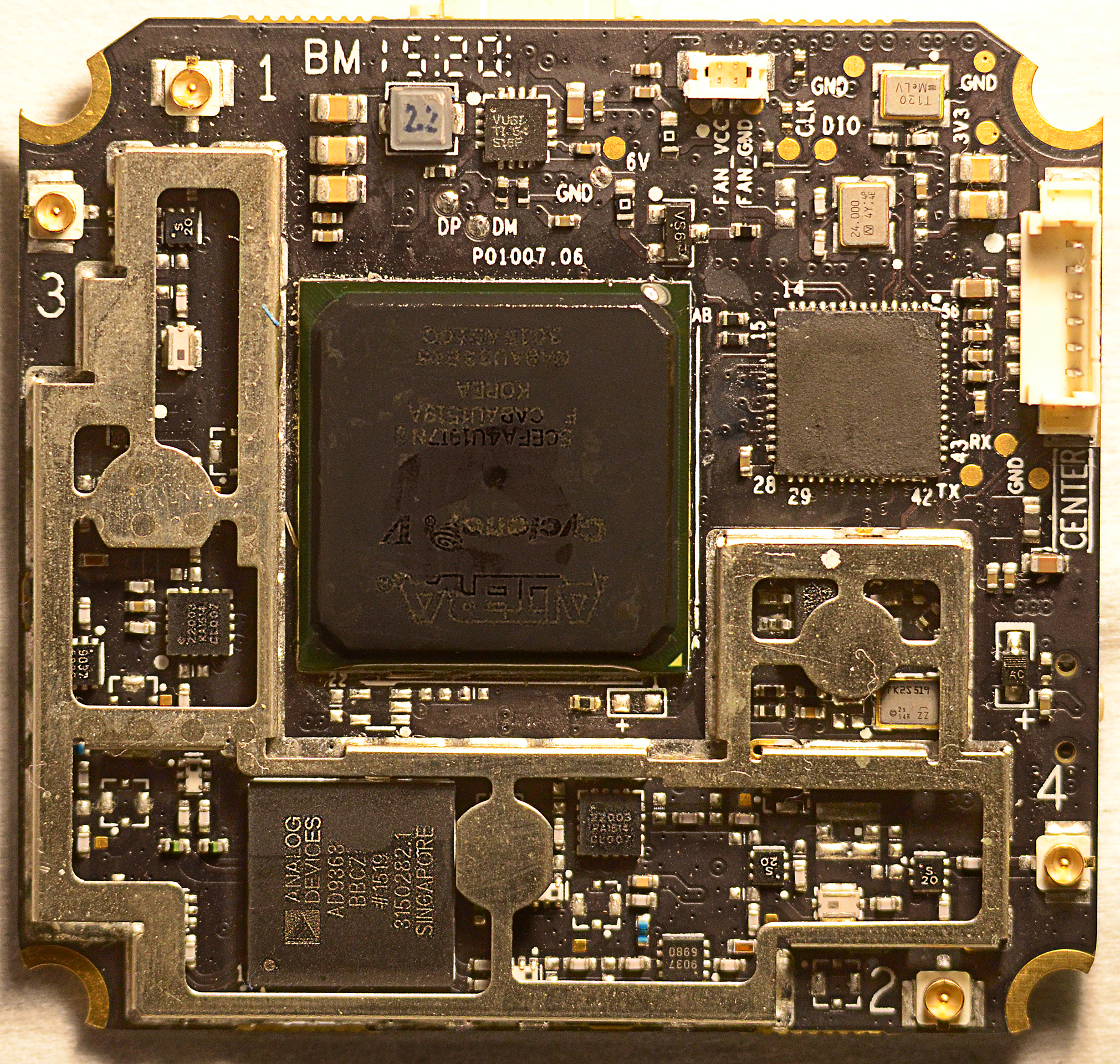
Top of a P01007.06 board:

Bottom of the P01007.06 board:
Top of a second P01007.06 board (poor image but visible behind shielding):
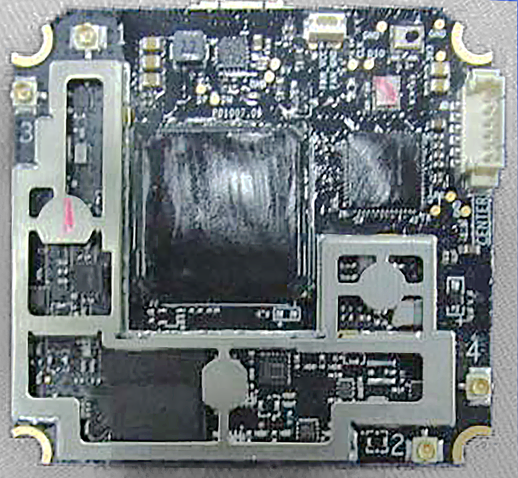
Bottom of the second P01007.06 board:

Top of a third P01007.06 board (more markings visible):
Bottom of the third P01007.06 board:
Top of a fourth P01007.06 board (FPGA marking visible):
Bottom of the fourth P01007.06 board:

Top of a P01007.08 board:

Bottom of the P01007.08 board:

Top of a P01007.14 board:

Bottom of the P01007.14 board:

flowchart LR
    Ribbon-Gimbal((ribbon<br/>to<br/>Gimbal))
    Ribbon-Center((ribbon<br/>to ESC<br/>Center))
    Ribbon-Gimbal== video<br/>over<br/>USB ===USB-Deserializer
    Ribbon-Gimbal-- CAN<br/>DUML ---OFDM-CAN-trx
    Ribbon-Center-- UART<br/>DUML ----Lightbridge-MCU
    subgraph OFDM Receiver board
    USB-Deserializer[Cypress<br/>FX2LP USB<br/>deserializer]
    Data-Scrambler[Altera FPGA<br/>or Artosyn ASIC<br/>data encoder/<br/>scrambler]
    Lightbridge-MCU[Lightbridge<br/>MCU]
    Serial-Flash[Serial<br/>flash]
    OFDM-CAN-trx[CAN<br/>tx/rx]
    WiMAX-Transceiver[WiMAX<br/>double<br/>transceiver]
    Lightbridge-MCU-- tx config<br/>and DUML ---Data-Scrambler
    Lightbridge-MCU-- radio config<br/>via SPI ---WiMAX-Transceiver
    OFDM-CAN-trx---Lightbridge-MCU
    Serial-Flash-- FW<br/>update ---Lightbridge-MCU
    Serial-Flash-- bitstream ---Data-Scrambler
    USB-Deserializer===Data-Scrambler
    Data-Scrambler===WiMAX-Transceiver
    WiMAX-Transceiver===RF-Tx-Amp-A[RF power<br/>out amp]
    WiMAX-Transceiver---RF-Rx-Amp-A[RF LNA<br/>inp amp]
    WiMAX-Transceiver===RF-Tx-Amp-B[RF power<br/>out amp]
    WiMAX-Transceiver---RF-Rx-Amp-B[RF LNA<br/>inp amp]
    RF-Switch-A[RF<br/>switch]
    RF-Switch-B[RF<br/>switch]
    RF-Tx-Amp-A===RF-Switch-A
    RF-Rx-Amp-A---RF-Switch-A
    RF-Tx-Amp-B===RF-Switch-B
    RF-Rx-Amp-B---RF-Switch-B
    end
    Antenna-A1((Ant))
    Antenna-A2((Ant))
    Antenna-B1((Ant))
    Antenna-B2((Ant))
    RF-Switch-A---Antenna-A1
    RF-Switch-A---Antenna-A2
    RF-Switch-B---Antenna-B1
    RF-Switch-B---Antenna-B2
Thick lines present propagation of video data. The live video feed comes from Gimbal top board through ribbon cable. It is wrapped with USB packets, so first the USB deserializer handles it and prepares input data for the FPGA. The FPGA, during power-on initialization, loaded a bitstream from Serial Flash, and became a digital data scrambler for the Lightbridge protocol. It prepares the video data and telemetry to be sent through radio channel, and supplies it to WiMAX Transceiver, from where the modulated signal is amplified and sent toward antennas.
The antennas can also receive DUML packets from the RC, in which case the input RF signal is amplified through LNA, received through WiMAX Transceiver, and provided to the FPGA for error correction and unscrambling. The DUML packets are provided to the Lightbridge Main Controller Unit, and from there routed either to Flight Controller on ESC center board or to Gimbal top board.
The MCU micro-controller is responsible for configuring the transmission by sending SPI commands to the WiMAX Transceiver, and setting logic signals on some configuration lines of the FPGA. In case of firmware update, the MCU accepts not only its own firmware, but also flashes the chip containing FPGA bitstream. Surprisingly, it does not update the firmware of the USB deserializer - that is routed through the Gimbal board and DaVinci chip, and reaches its destination through the USB link, the same one which transfers live video feed data.
Two chips on the board have cheaper substitutes, used in later versions of the board:
- WiMAX transceiver, instead of AD9363, can be much more noisy AR8003.
- Altera FPGA can be replaced by ASIC which implements the exact same functionality, AR8001. In such case, Serial flash is no longer in use, but it is left on the board to avoid the need of further changes in software of the MCU.
The following schematics were made by enthusiasts: