Repository navigation
Feature Test Collection
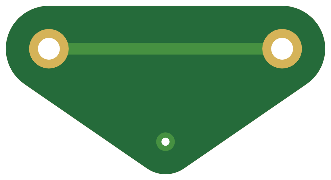
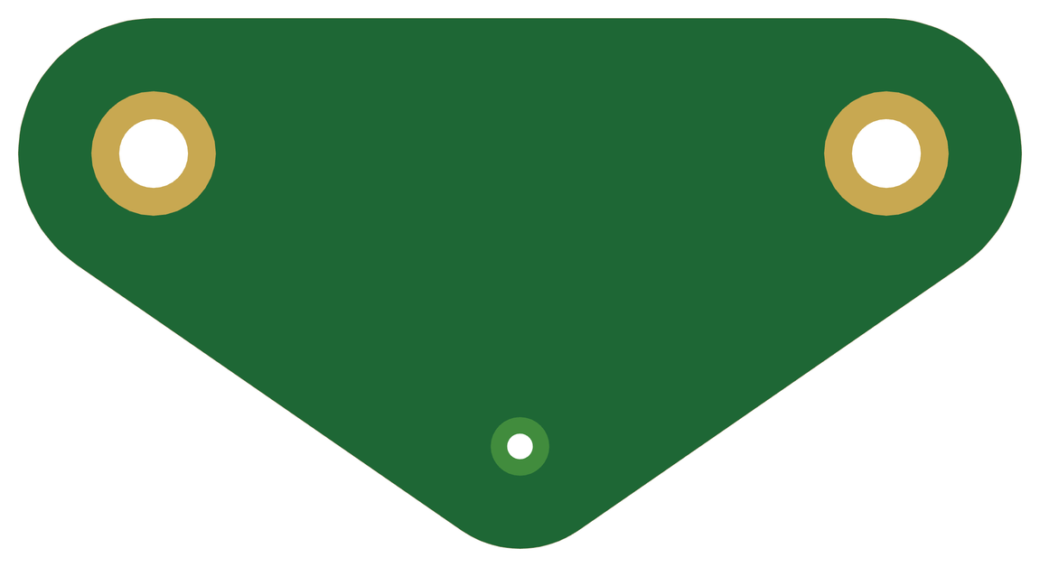
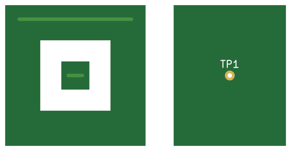
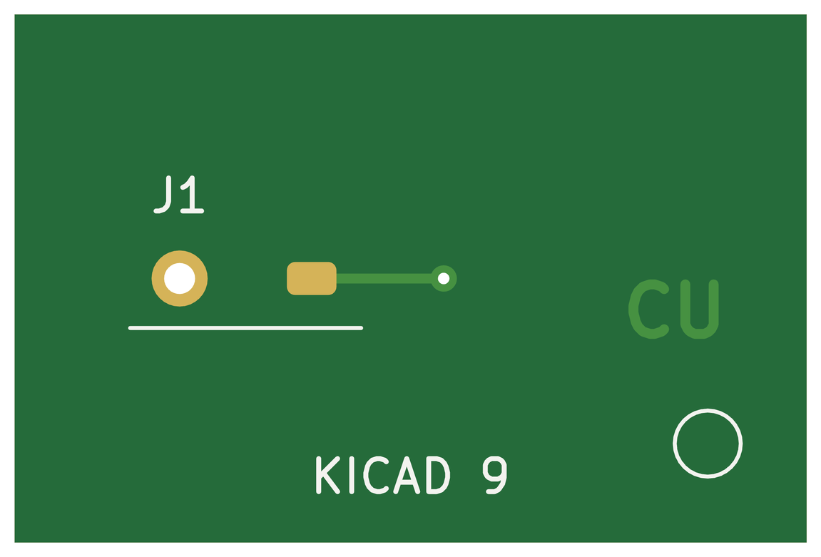
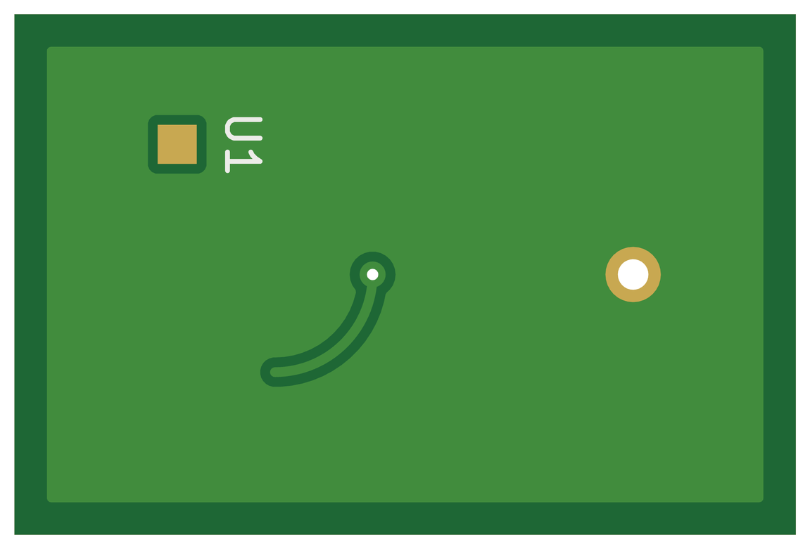
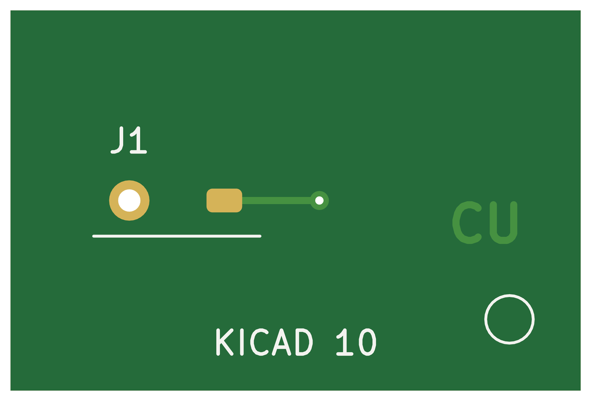
Every board of featureTest/, section by section, with its top and bottom and where the time of a
run goes:
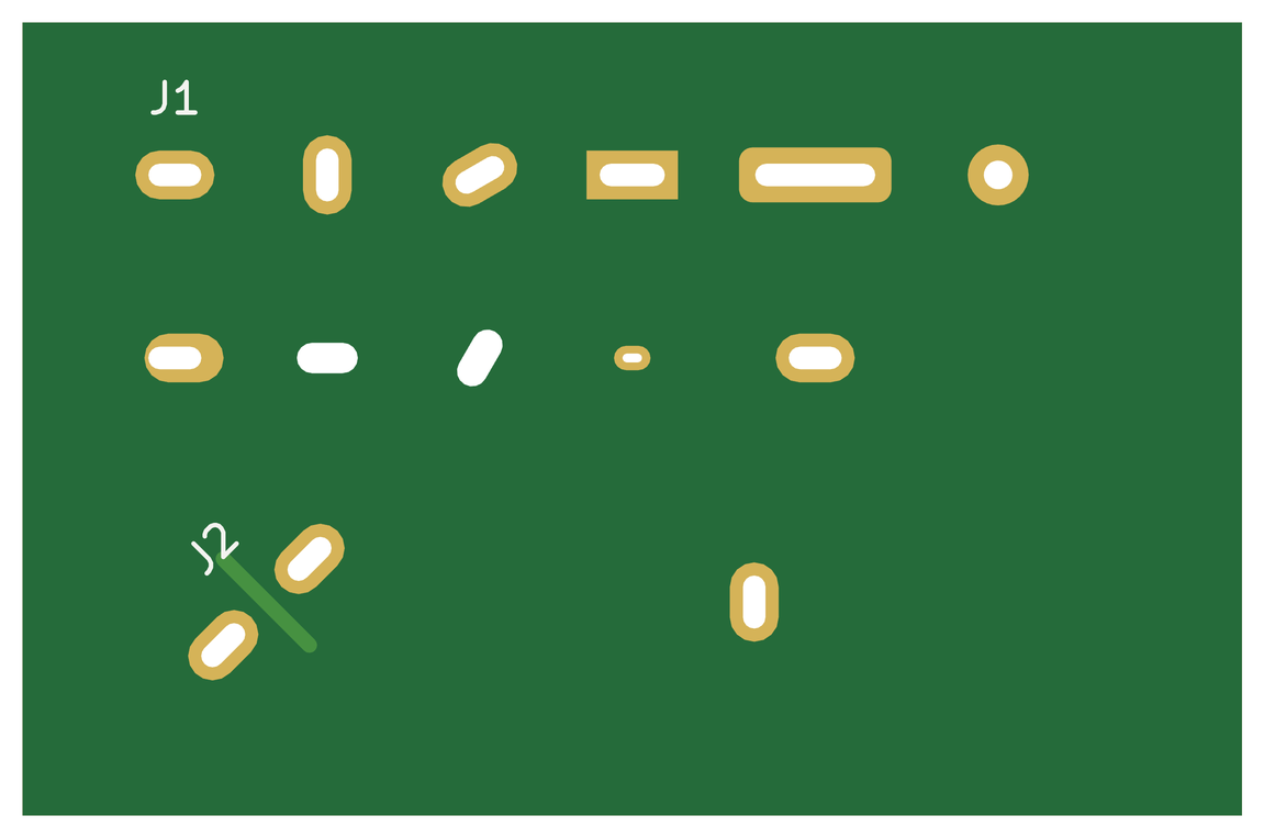
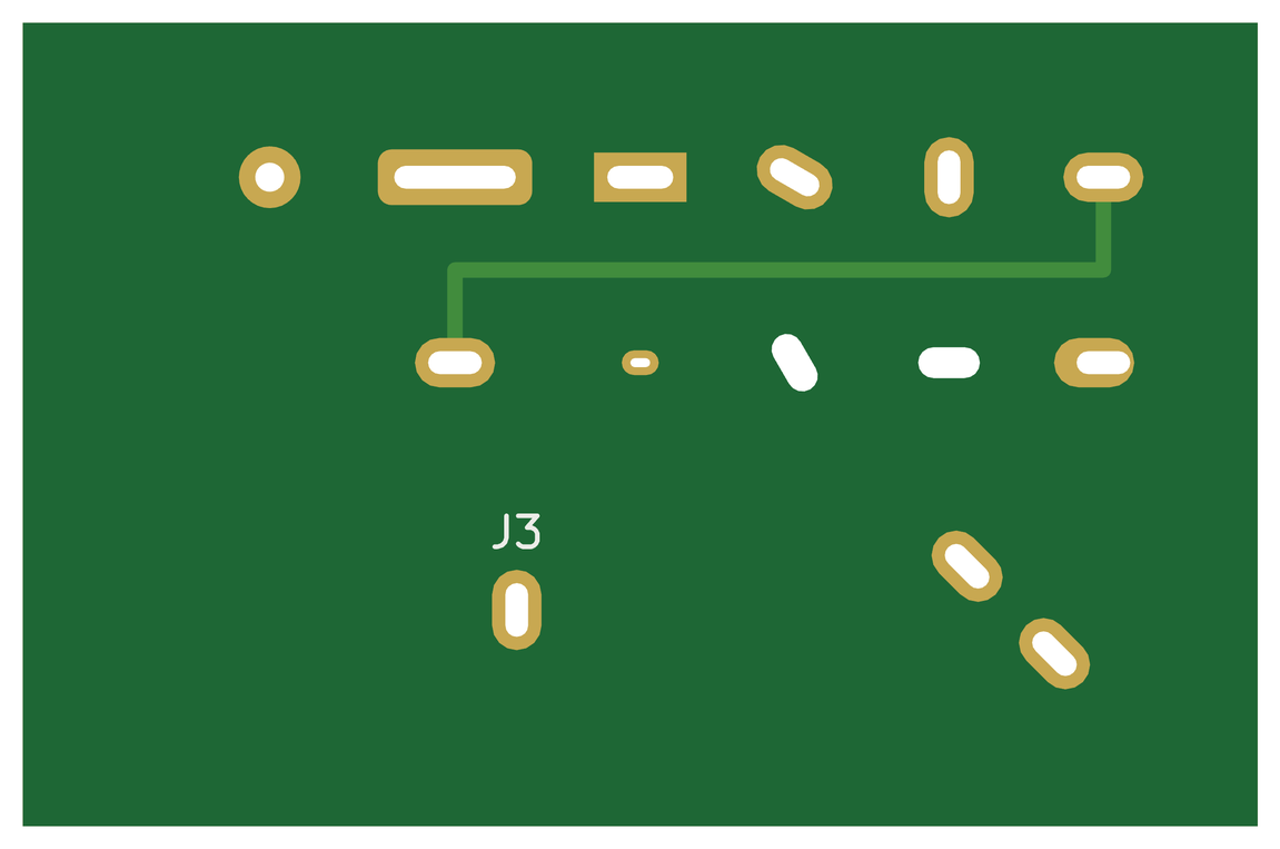
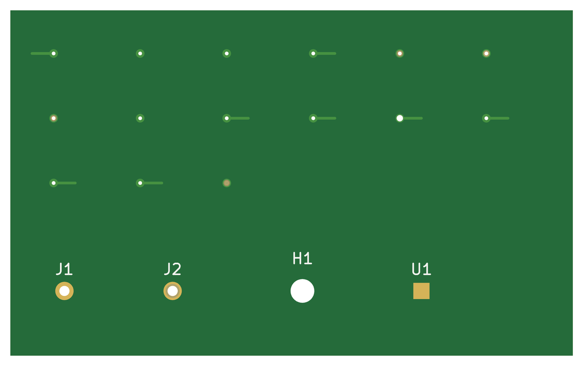
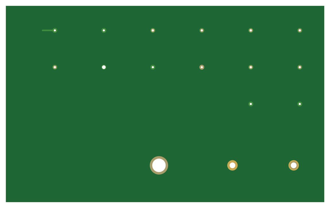
- The folder's README says what each board holds.
- Each board was exported in every format KESE writes, one format a run: GLB, STEP, STL and OBJ in
simulation mode, and GLB and OBJ in visual mode. Each of those six runs was made three times, with
the Verifier, the solder mask and the silkscreen on and the board's own settings, as the
regression suite (
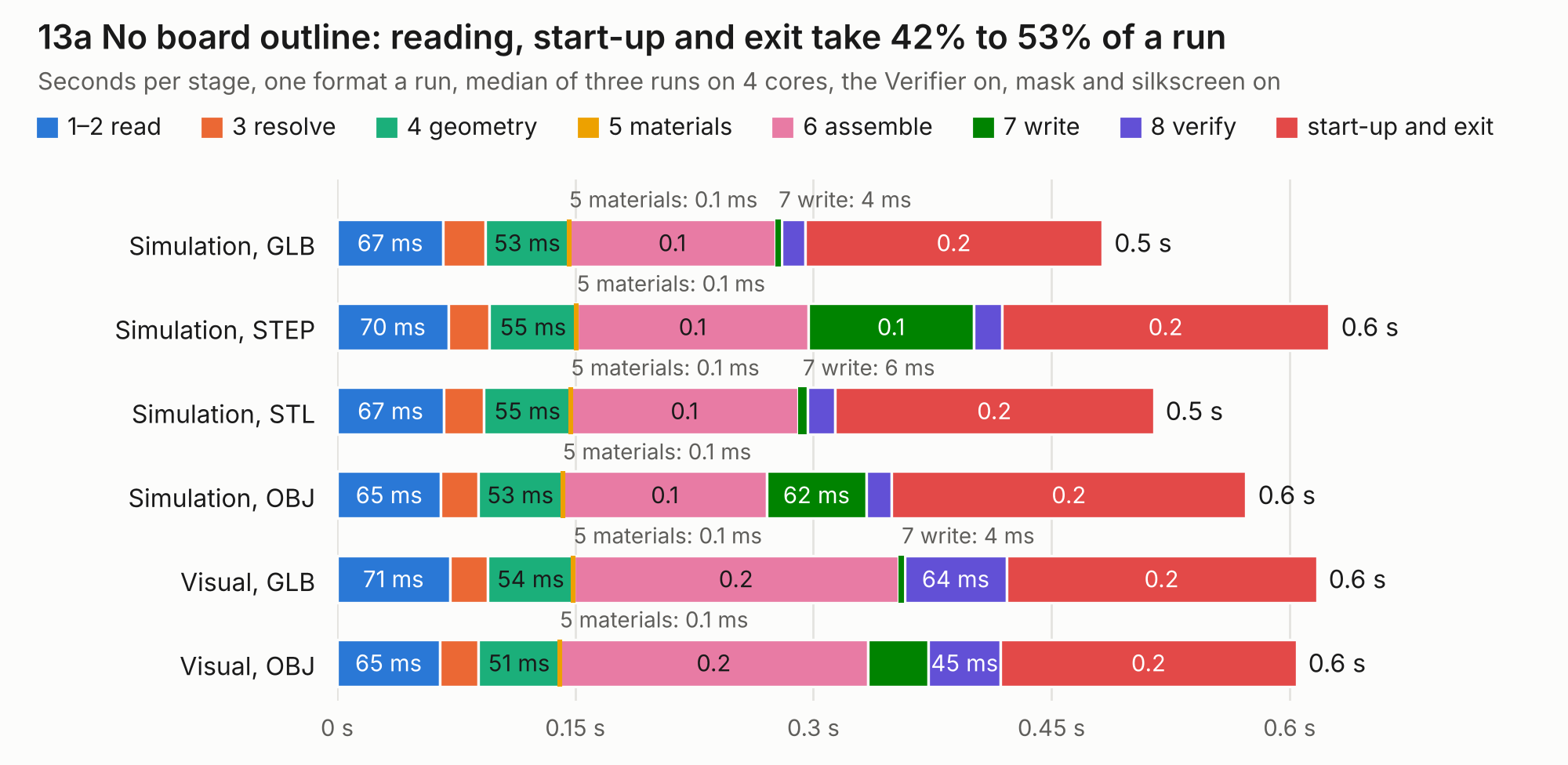
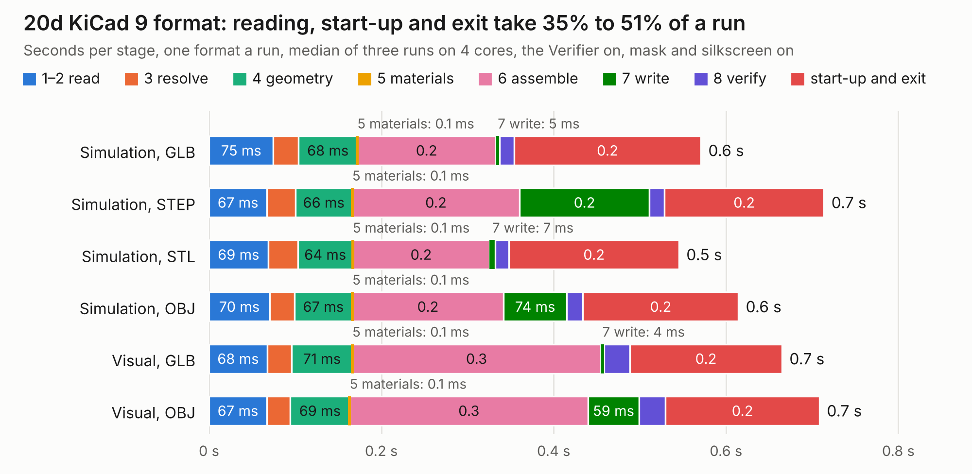
Generator/tests/test_boards.py) sets them. - Each bar is the median of the three runs for that stage, from the
timingblock ofreport.txt. All 720 runs passed the Verifier. - Beside each board's facts, a second table gives, for each of the six runs, the size of the model
file it writes and the most memory it used at once: the proportional set size (PSS) of KESE's
process and its workers, summed and sampled every 10 ms, the median of three more runs. The STL
size is that of the
stl/folder, one file a part, and the OBJ size includes its.mtl. MB is a million bytes. - The command for board 11, simulation mode with GLB; the other five runs differ only in
--format step,stlorobj, or in--mode visualwith--format glborobj:
python run_KESE.py ../featureTest/11_zones.kicad_pcb --mode simulation --format glb --verify \
    --set SolderMask.SOLDER_MASK_ENABLED=True --set Silkscreen.SILKSCREEN_ENABLED=True
The runs used the default parameters otherwise, on one Linux machine with 4 cores (an Intel Xeon
at 2.1 GHz) and 16 GB of RAM, so Parallel.WORKERS = 0 gave four workers (Work Done In
Parallel). On another machine the seconds differ.
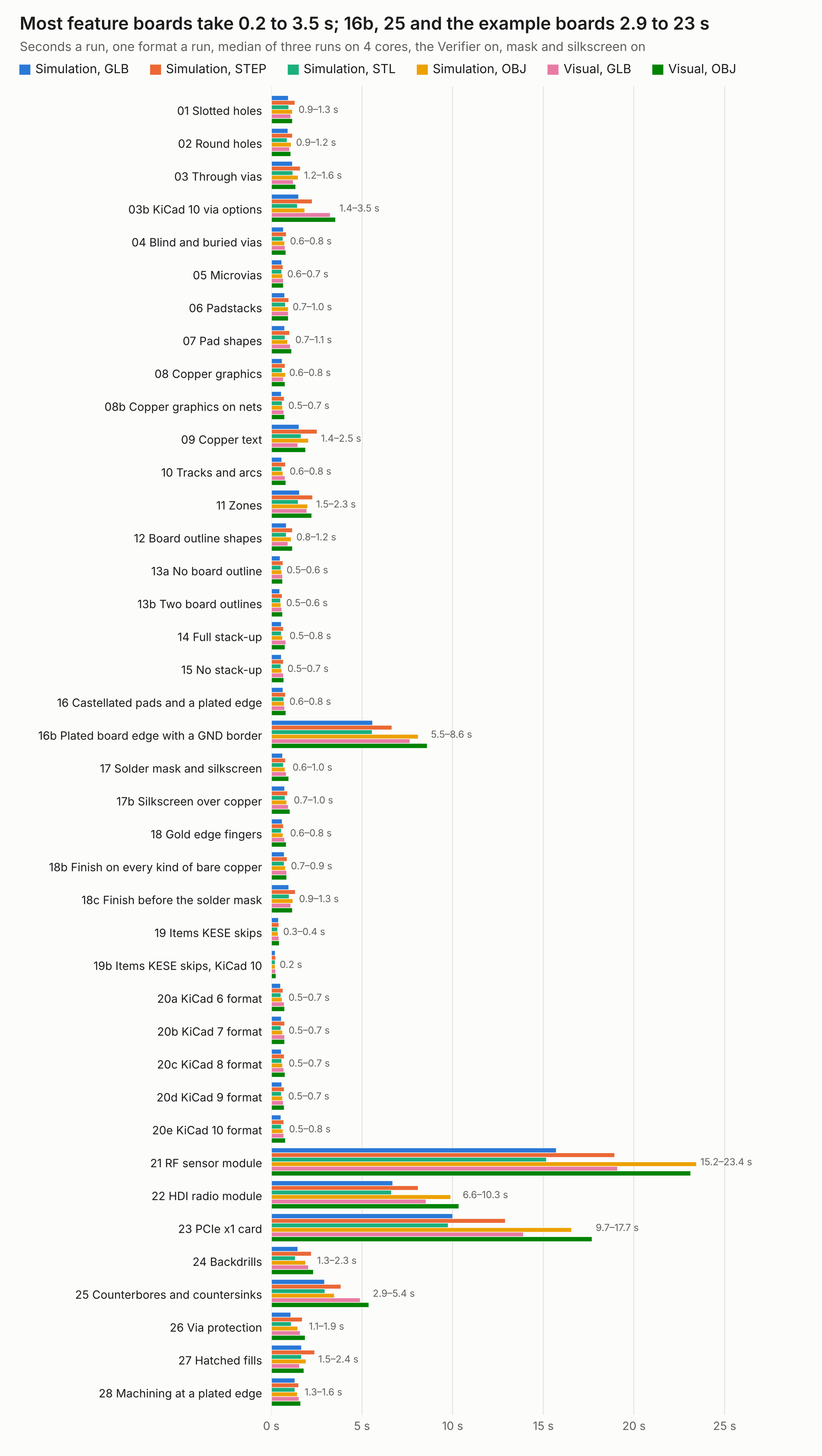
All the feature boards but 16b and 25 take 0.2 to 3.5 s a run, in any format. The fixed part of a run, reading the file and Python starting and exiting, takes 0.16 to 0.33 s of it; a board without text never reads the stroke font, so boards 05, 08b, 19b and 26 read and collect in under 11 ms. Board 16b, a plated border and 91 vias on four layers, takes 5.6 to 8.6 s; board 25, whose countersinks are built as steps, 2.9 to 5.4 s; and the example boards 6.6 to 23.4 s. Simulation with GLB or STL is the quickest of the six runs on every board but 09 and 27, where visual GLB is.
| Mode and format | 1–2 read | 3 resolve | 4 geometry | 5 materials | 6 assemble | 7 write | 8 verify | start-up and exit | Total |
|---|---|---|---|---|---|---|---|---|---|
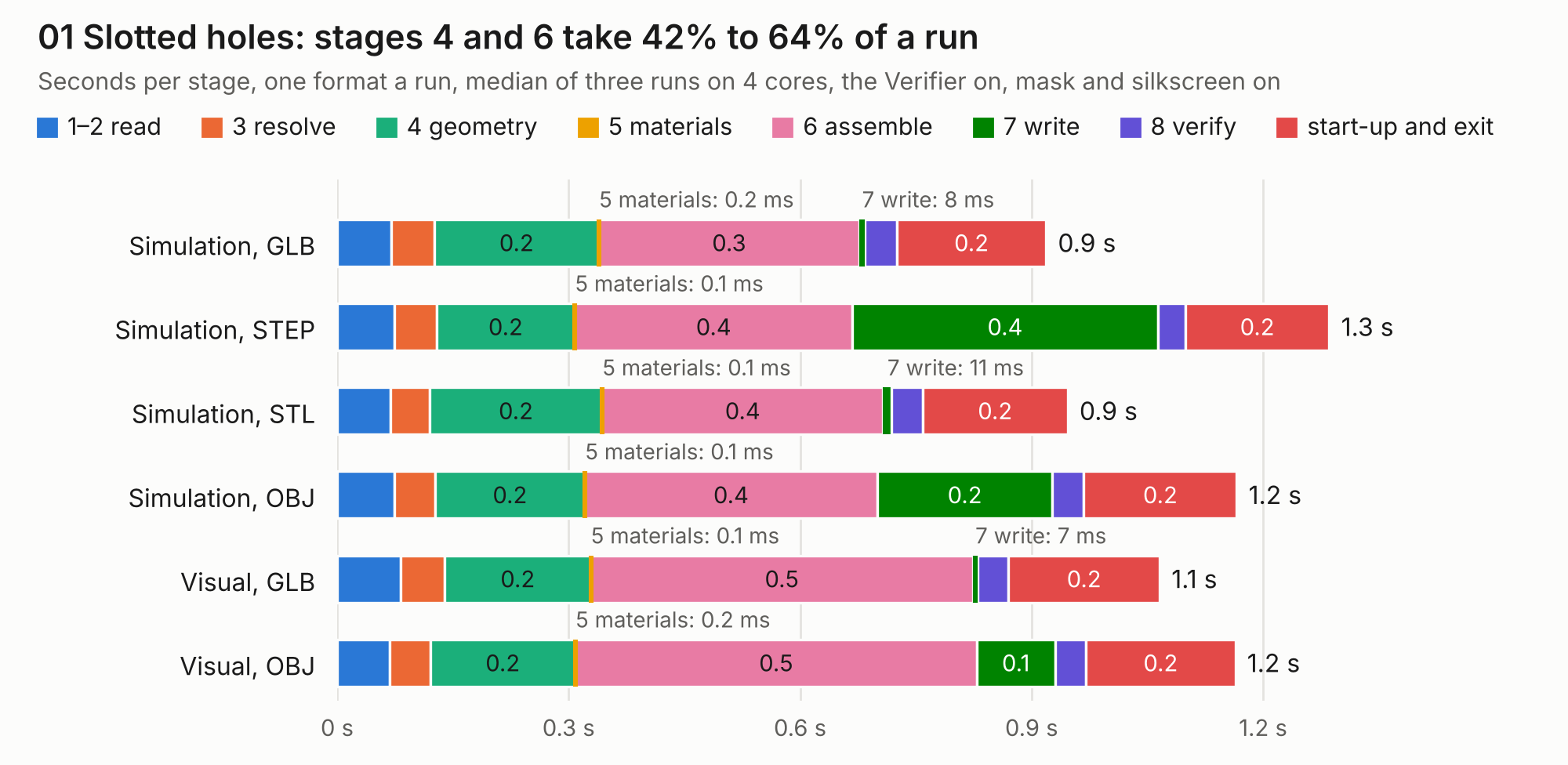
| Simulation, GLB | 70 ms | 56 ms | 0.2 | 0.2 ms | 0.3 | 8 ms | 41 ms | 0.2 | 0.9 |
| Simulation, STEP | 74 ms | 55 ms | 0.2 | 0.1 ms | 0.4 | 0.4 | 36 ms | 0.2 | 1.3 |
| Simulation, STL | 69 ms | 51 ms | 0.2 | 0.1 ms | 0.4 | 11 ms | 40 ms | 0.2 | 0.9 |
| Simulation, OBJ | 74 ms | 53 ms | 0.2 | 0.1 ms | 0.4 | 0.2 | 41 ms | 0.2 | 1.2 |
| Visual, GLB | 83 ms | 56 ms | 0.2 | 0.1 ms | 0.5 | 7 ms | 40 ms | 0.2 | 1.1 |
| Visual, OBJ | 68 ms | 53 ms | 0.2 | 0.2 ms | 0.5 | 0.1 | 40 ms | 0.2 | 1.2 |
|
|
|||||||||||||||||||||||||||||||||||||||||
| Mode and format | 1–2 read | 3 resolve | 4 geometry | 5 materials | 6 assemble | 7 write | 8 verify | start-up and exit | Total |
|---|---|---|---|---|---|---|---|---|---|
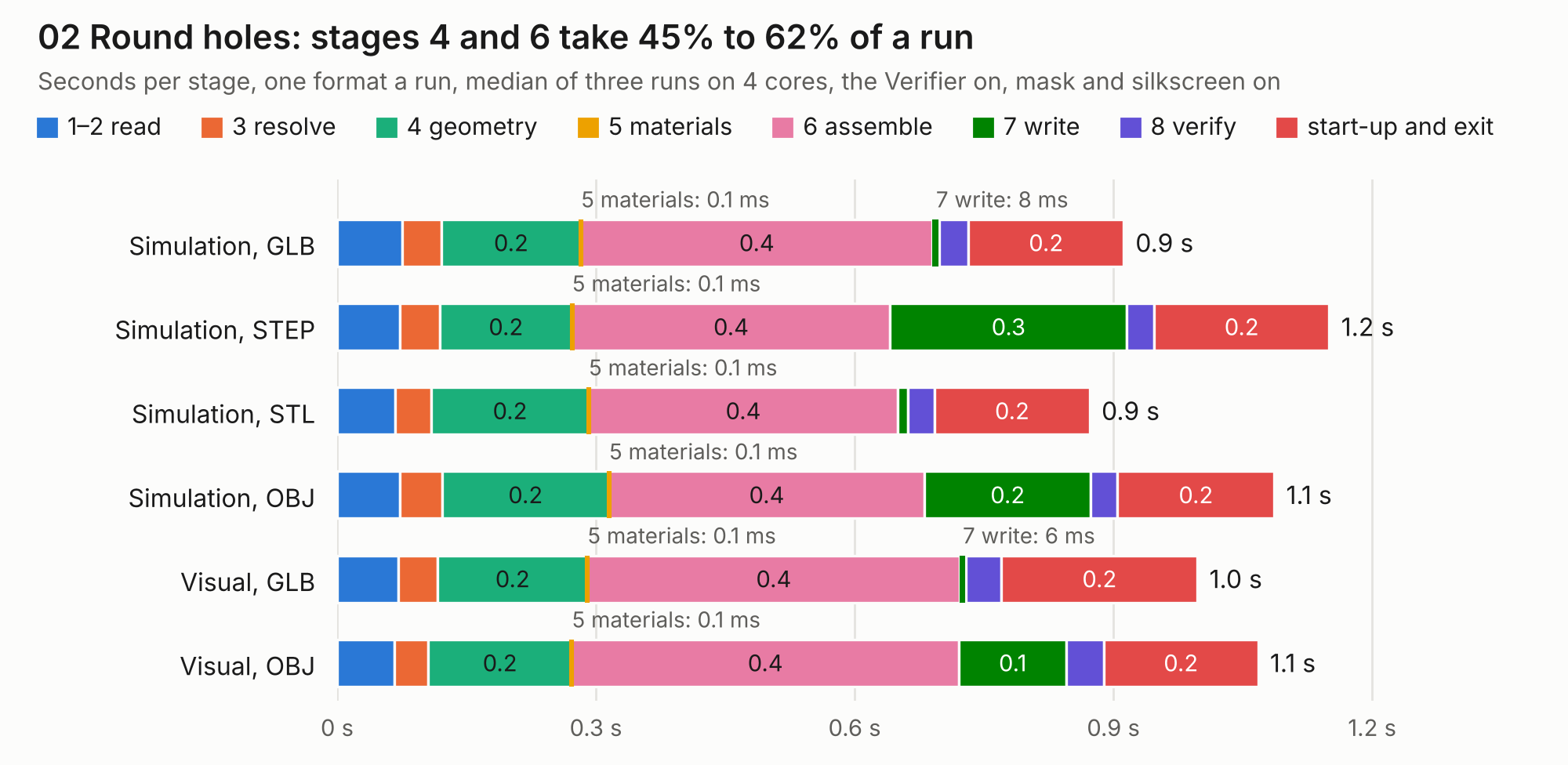
| Simulation, GLB | 76 ms | 45 ms | 0.2 | 0.1 ms | 0.4 | 8 ms | 34 ms | 0.2 | 0.9 |
| Simulation, STEP | 73 ms | 46 ms | 0.2 | 0.1 ms | 0.4 | 0.3 | 31 ms | 0.2 | 1.2 |
| Simulation, STL | 67 ms | 42 ms | 0.2 | 0.1 ms | 0.4 | 12 ms | 31 ms | 0.2 | 0.9 |
| Simulation, OBJ | 72 ms | 49 ms | 0.2 | 0.1 ms | 0.4 | 0.2 | 31 ms | 0.2 | 1.1 |
| Visual, GLB | 71 ms | 46 ms | 0.2 | 0.1 ms | 0.4 | 6 ms | 42 ms | 0.2 | 1.0 |
| Visual, OBJ | 66 ms | 39 ms | 0.2 | 0.1 ms | 0.4 | 0.1 | 43 ms | 0.2 | 1.1 |
|
|
|||||||||||||||||||||||||||||||||||||||||
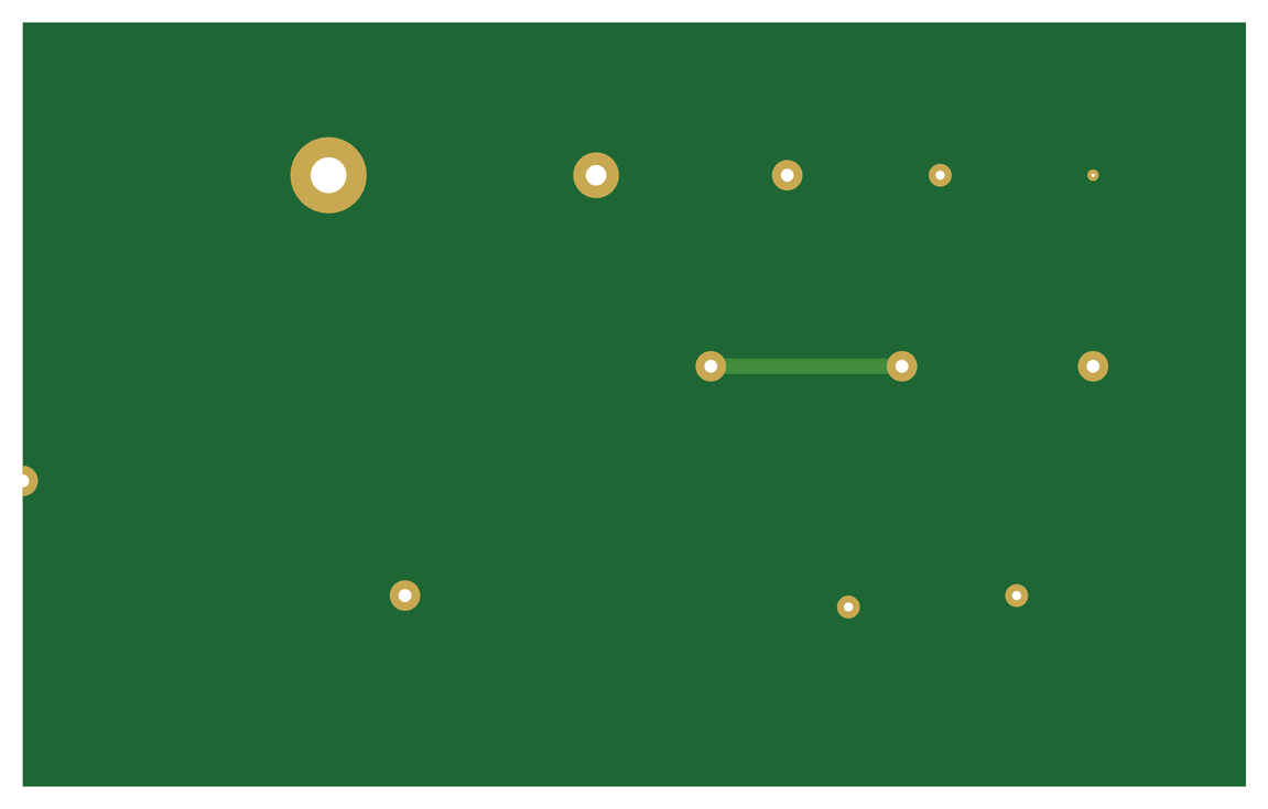
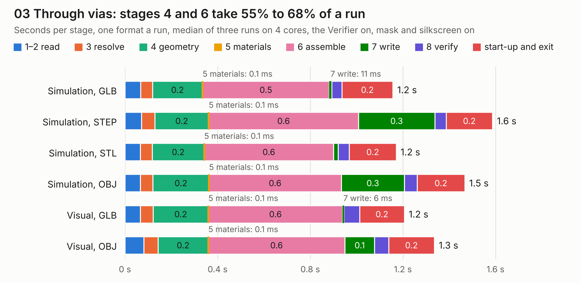
| Mode and format | 1–2 read | 3 resolve | 4 geometry | 5 materials | 6 assemble | 7 write | 8 verify | start-up and exit | Total |
|---|---|---|---|---|---|---|---|---|---|
| Simulation, GLB | 67 ms | 51 ms | 0.2 | 0.1 ms | 0.5 | 11 ms | 44 ms | 0.2 | 1.2 |
| Simulation, STEP | 71 ms | 58 ms | 0.2 | 0.1 ms | 0.6 | 0.3 | 49 ms | 0.2 | 1.6 |
| Simulation, STL | 67 ms | 51 ms | 0.2 | 0.1 ms | 0.6 | 20 ms | 48 ms | 0.2 | 1.2 |
| Simulation, OBJ | 66 ms | 55 ms | 0.2 | 0.1 ms | 0.6 | 0.3 | 55 ms | 0.2 | 1.5 |
| Visual, GLB | 67 ms | 55 ms | 0.2 | 0.1 ms | 0.6 | 6 ms | 67 ms | 0.2 | 1.2 |
| Visual, OBJ | 82 ms | 60 ms | 0.2 | 0.1 ms | 0.6 | 0.1 | 60 ms | 0.2 | 1.3 |
|
|
|||||||||||||||||||||||||||||||||||||||||
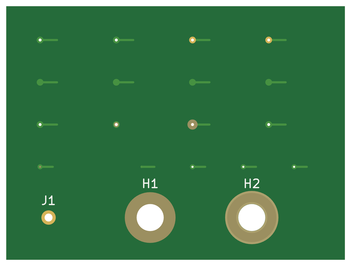
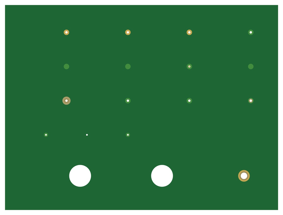
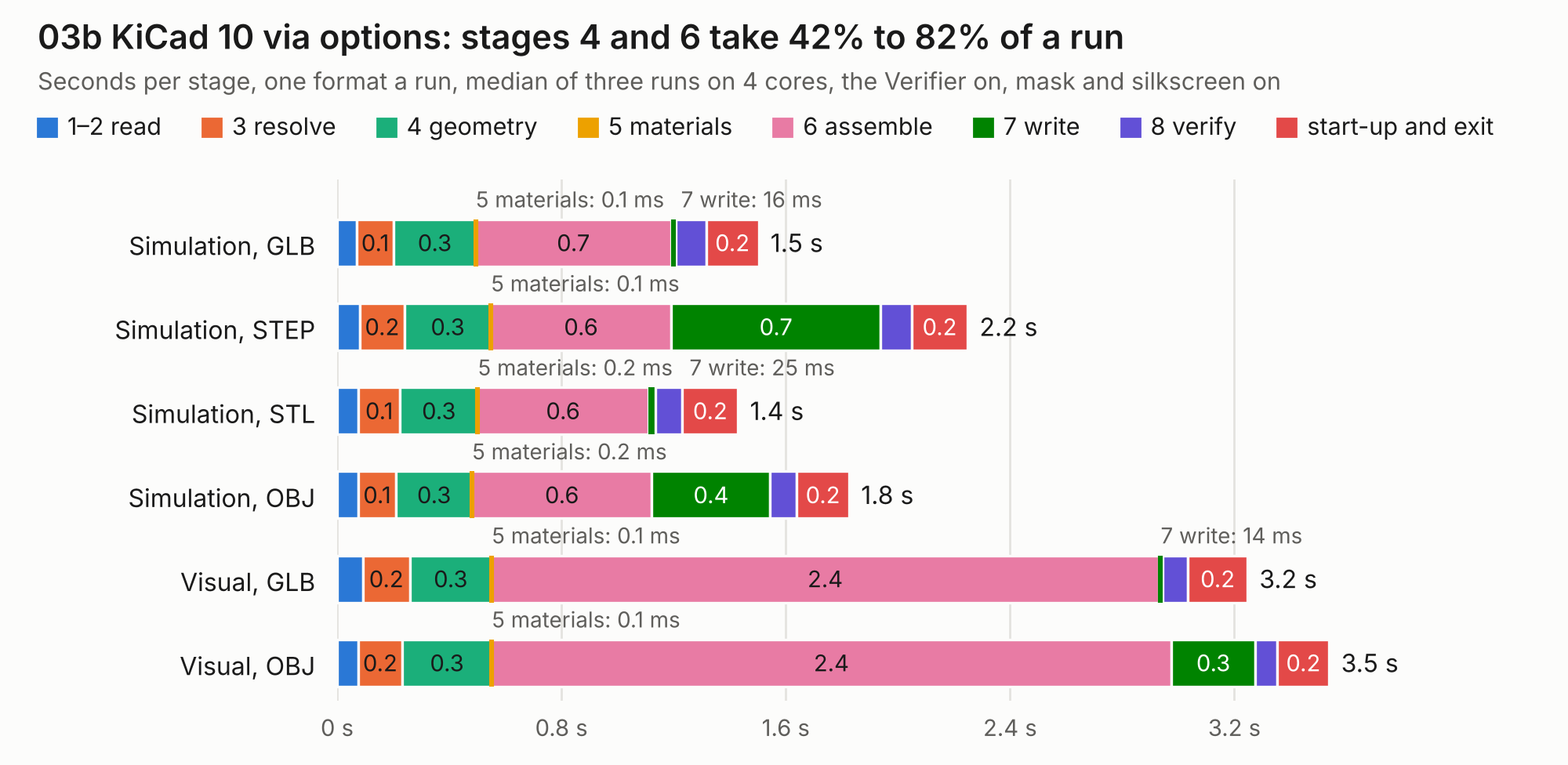
| Mode and format | 1–2 read | 3 resolve | 4 geometry | 5 materials | 6 assemble | 7 write | 8 verify | start-up and exit | Total |
|---|---|---|---|---|---|---|---|---|---|
| Simulation, GLB | 69 ms | 0.1 | 0.3 | 0.1 ms | 0.7 | 16 ms | 0.1 | 0.2 | 1.5 |
| Simulation, STEP | 80 ms | 0.2 | 0.3 | 0.1 ms | 0.6 | 0.7 | 0.1 | 0.2 | 2.2 |
| Simulation, STL | 76 ms | 0.1 | 0.3 | 0.2 ms | 0.6 | 25 ms | 97 ms | 0.2 | 1.4 |
| Simulation, OBJ | 75 ms | 0.1 | 0.3 | 0.2 ms | 0.6 | 0.4 | 94 ms | 0.2 | 1.8 |
| Visual, GLB | 92 ms | 0.2 | 0.3 | 0.1 ms | 2.4 | 14 ms | 90 ms | 0.2 | 3.2 |
| Visual, OBJ | 74 ms | 0.2 | 0.3 | 0.1 ms | 2.4 | 0.3 | 78 ms | 0.2 | 3.5 |
|
|
|||||||||||||||||||||||||||||||||||||||||
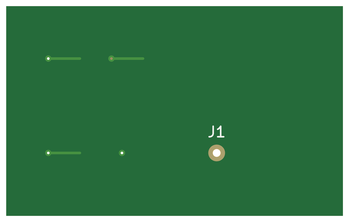
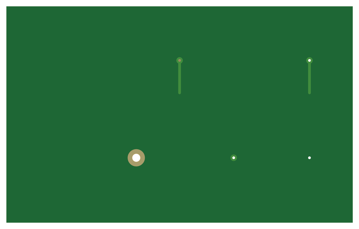
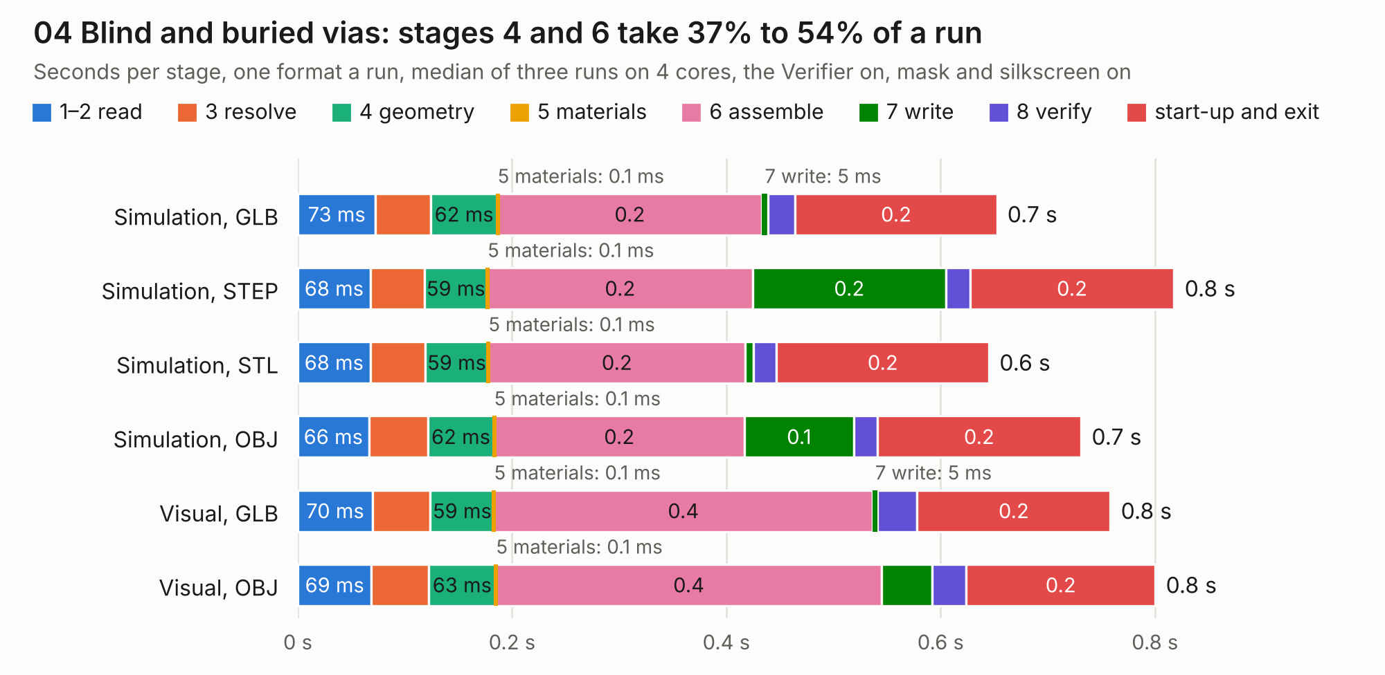
| Mode and format | 1–2 read | 3 resolve | 4 geometry | 5 materials | 6 assemble | 7 write | 8 verify | start-up and exit | Total |
|---|---|---|---|---|---|---|---|---|---|
| Simulation, GLB | 73 ms | 51 ms | 62 ms | 0.1 ms | 0.2 | 5 ms | 26 ms | 0.2 | 0.7 |
| Simulation, STEP | 68 ms | 50 ms | 59 ms | 0.1 ms | 0.2 | 0.2 | 22 ms | 0.2 | 0.8 |
| Simulation, STL | 68 ms | 51 ms | 59 ms | 0.1 ms | 0.2 | 8 ms | 21 ms | 0.2 | 0.6 |
| Simulation, OBJ | 66 ms | 55 ms | 62 ms | 0.1 ms | 0.2 | 0.1 | 22 ms | 0.2 | 0.7 |
| Visual, GLB | 70 ms | 54 ms | 59 ms | 0.1 ms | 0.4 | 5 ms | 37 ms | 0.2 | 0.8 |
| Visual, OBJ | 69 ms | 53 ms | 63 ms | 0.1 ms | 0.4 | 47 ms | 32 ms | 0.2 | 0.8 |
|
|
|||||||||||||||||||||||||||||||||||||||||


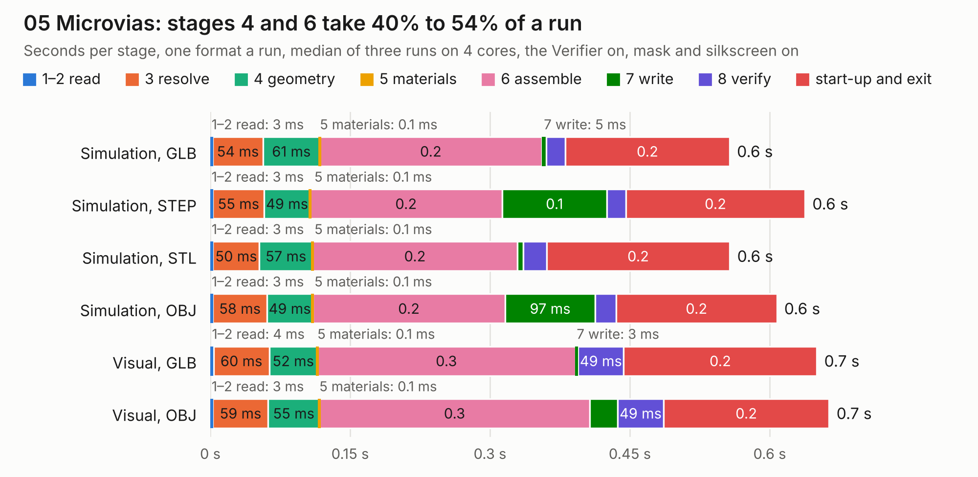
| Mode and format | 1–2 read | 3 resolve | 4 geometry | 5 materials | 6 assemble | 7 write | 8 verify | start-up and exit | Total |
|---|---|---|---|---|---|---|---|---|---|
| Simulation, GLB | 3 ms | 54 ms | 61 ms | 0.1 ms | 0.2 | 5 ms | 21 ms | 0.2 | 0.6 |
| Simulation, STEP | 3 ms | 55 ms | 49 ms | 0.1 ms | 0.2 | 0.1 | 20 ms | 0.2 | 0.6 |
| Simulation, STL | 3 ms | 50 ms | 57 ms | 0.1 ms | 0.2 | 6 ms | 25 ms | 0.2 | 0.6 |
| Simulation, OBJ | 3 ms | 58 ms | 49 ms | 0.1 ms | 0.2 | 97 ms | 22 ms | 0.2 | 0.6 |
| Visual, GLB | 4 ms | 60 ms | 52 ms | 0.1 ms | 0.3 | 3 ms | 49 ms | 0.2 | 0.7 |
| Visual, OBJ | 3 ms | 59 ms | 55 ms | 0.1 ms | 0.3 | 30 ms | 49 ms | 0.2 | 0.7 |
|
|
|||||||||||||||||||||||||||||||||||||||||
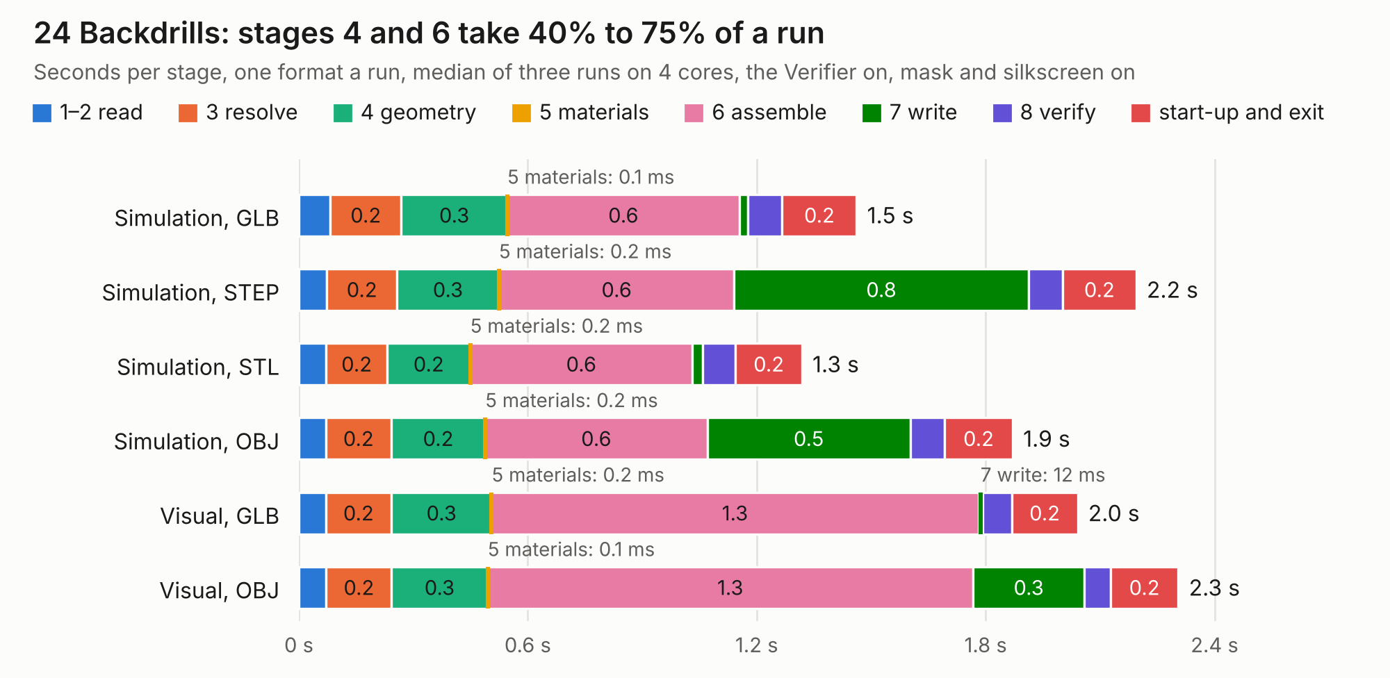
| Mode and format | 1–2 read | 3 resolve | 4 geometry | 5 materials | 6 assemble | 7 write | 8 verify | start-up and exit | Total |
|---|---|---|---|---|---|---|---|---|---|
| Simulation, GLB | 82 ms | 0.2 | 0.3 | 0.1 ms | 0.6 | 22 ms | 90 ms | 0.2 | 1.5 |
| Simulation, STEP | 73 ms | 0.2 | 0.3 | 0.2 ms | 0.6 | 0.8 | 90 ms | 0.2 | 2.2 |
| Simulation, STL | 72 ms | 0.2 | 0.2 | 0.2 ms | 0.6 | 28 ms | 86 ms | 0.2 | 1.3 |
| Simulation, OBJ | 70 ms | 0.2 | 0.2 | 0.2 ms | 0.6 | 0.5 | 90 ms | 0.2 | 1.9 |
| Visual, GLB | 70 ms | 0.2 | 0.3 | 0.2 ms | 1.3 | 12 ms | 75 ms | 0.2 | 2.0 |
| Visual, OBJ | 72 ms | 0.2 | 0.3 | 0.1 ms | 1.3 | 0.3 | 68 ms | 0.2 | 2.3 |
|
|
|||||||||||||||||||||||||||||||||||||||||
| Mode and format | 1–2 read | 3 resolve | 4 geometry | 5 materials | 6 assemble | 7 write | 8 verify | start-up and exit | Total |
|---|---|---|---|---|---|---|---|---|---|
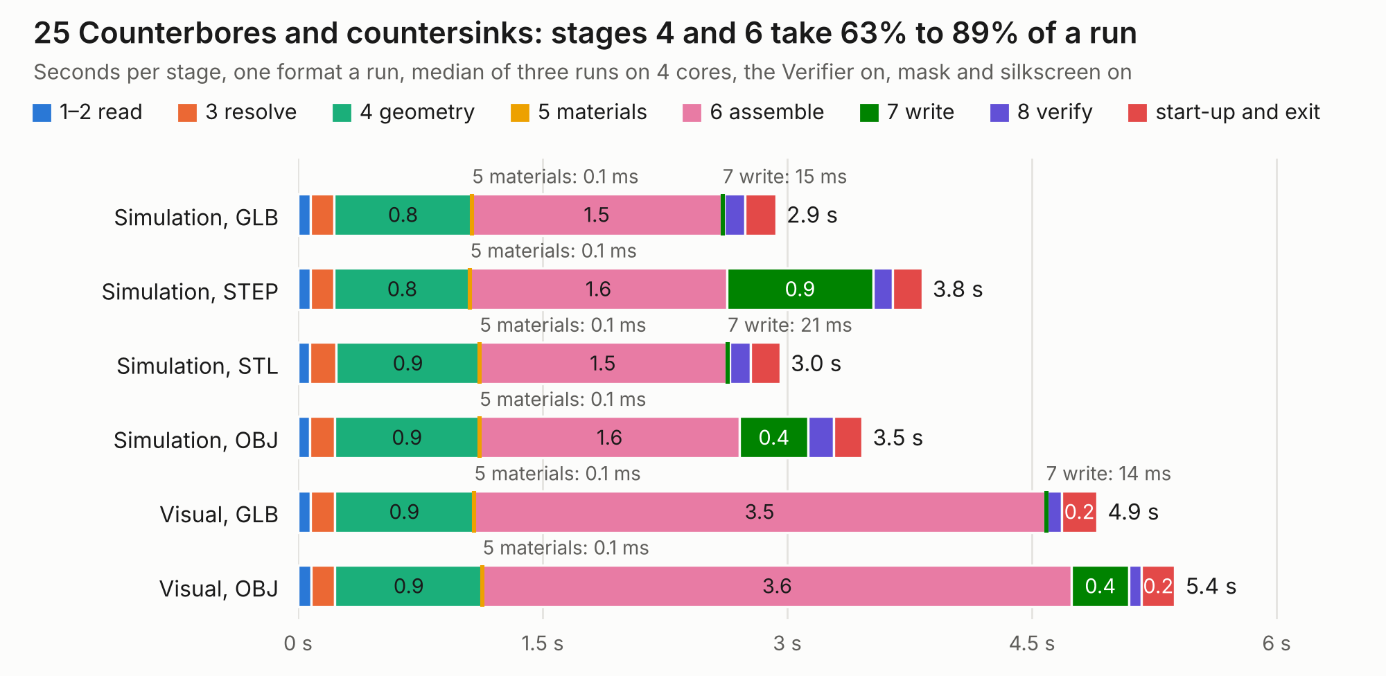
| Simulation, GLB | 76 ms | 0.1 | 0.8 | 0.1 ms | 1.5 | 15 ms | 0.1 | 0.2 | 2.9 |
| Simulation, STEP | 75 ms | 0.1 | 0.8 | 0.1 ms | 1.6 | 0.9 | 0.1 | 0.2 | 3.8 |
| Simulation, STL | 74 ms | 0.2 | 0.9 | 0.1 ms | 1.5 | 21 ms | 0.1 | 0.2 | 3.0 |
| Simulation, OBJ | 74 ms | 0.1 | 0.9 | 0.1 ms | 1.6 | 0.4 | 0.2 | 0.2 | 3.5 |
| Visual, GLB | 75 ms | 0.1 | 0.9 | 0.1 ms | 3.5 | 14 ms | 88 ms | 0.2 | 4.9 |
| Visual, OBJ | 81 ms | 0.1 | 0.9 | 0.1 ms | 3.6 | 0.4 | 77 ms | 0.2 | 5.4 |
|
|
|||||||||||||||||||||||||||||||||||||||||
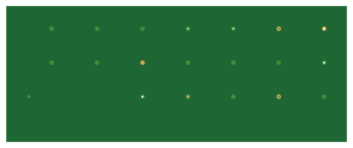
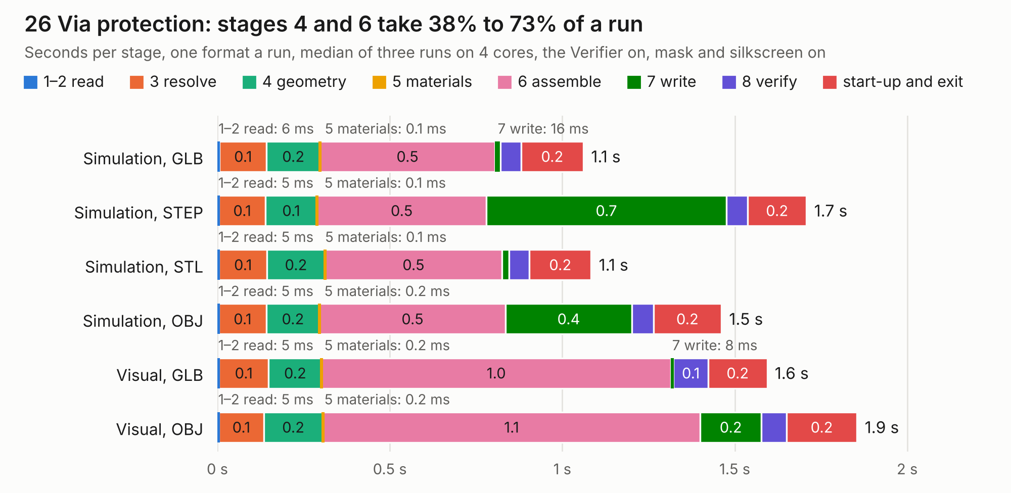
| Mode and format | 1–2 read | 3 resolve | 4 geometry | 5 materials | 6 assemble | 7 write | 8 verify | start-up and exit | Total |
|---|---|---|---|---|---|---|---|---|---|
| Simulation, GLB | 6 ms | 0.1 | 0.2 | 0.1 ms | 0.5 | 16 ms | 59 ms | 0.2 | 1.1 |
| Simulation, STEP | 5 ms | 0.1 | 0.1 | 0.1 ms | 0.5 | 0.7 | 62 ms | 0.2 | 1.7 |
| Simulation, STL | 5 ms | 0.1 | 0.2 | 0.1 ms | 0.5 | 20 ms | 59 ms | 0.2 | 1.1 |
| Simulation, OBJ | 5 ms | 0.1 | 0.2 | 0.2 ms | 0.5 | 0.4 | 62 ms | 0.2 | 1.5 |
| Visual, GLB | 5 ms | 0.1 | 0.2 | 0.2 ms | 1.0 | 8 ms | 0.1 | 0.2 | 1.6 |
| Visual, OBJ | 5 ms | 0.1 | 0.2 | 0.2 ms | 1.1 | 0.2 | 73 ms | 0.2 | 1.9 |
|
|
|||||||||||||||||||||||||||||||||||||||||
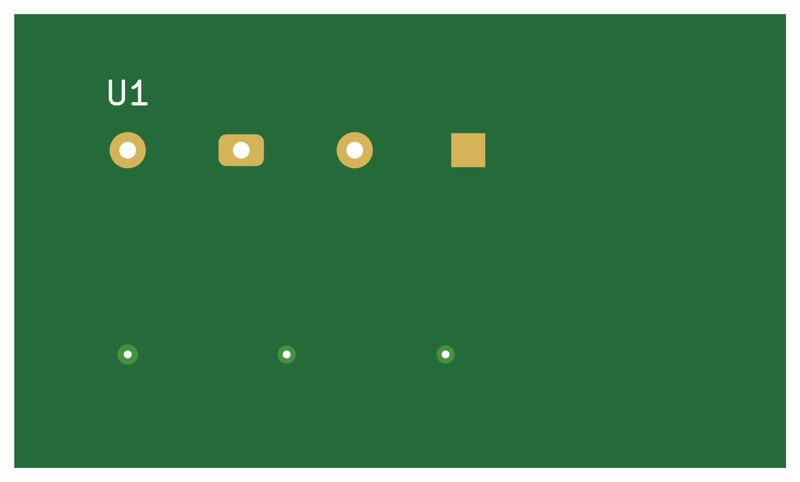
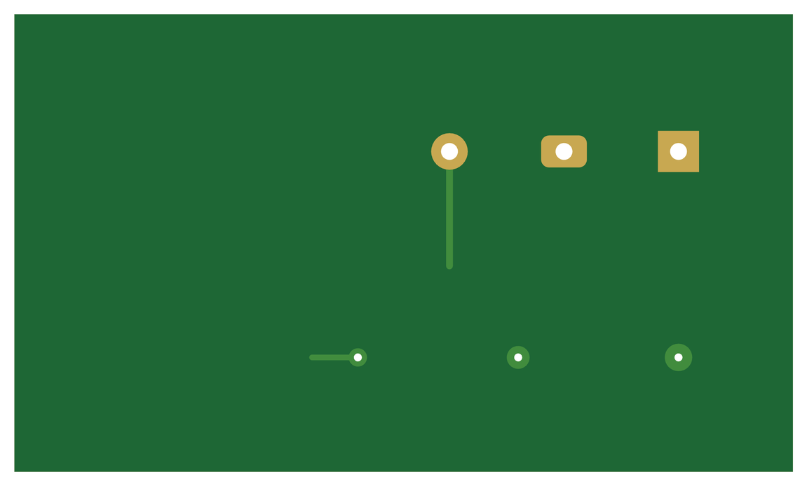
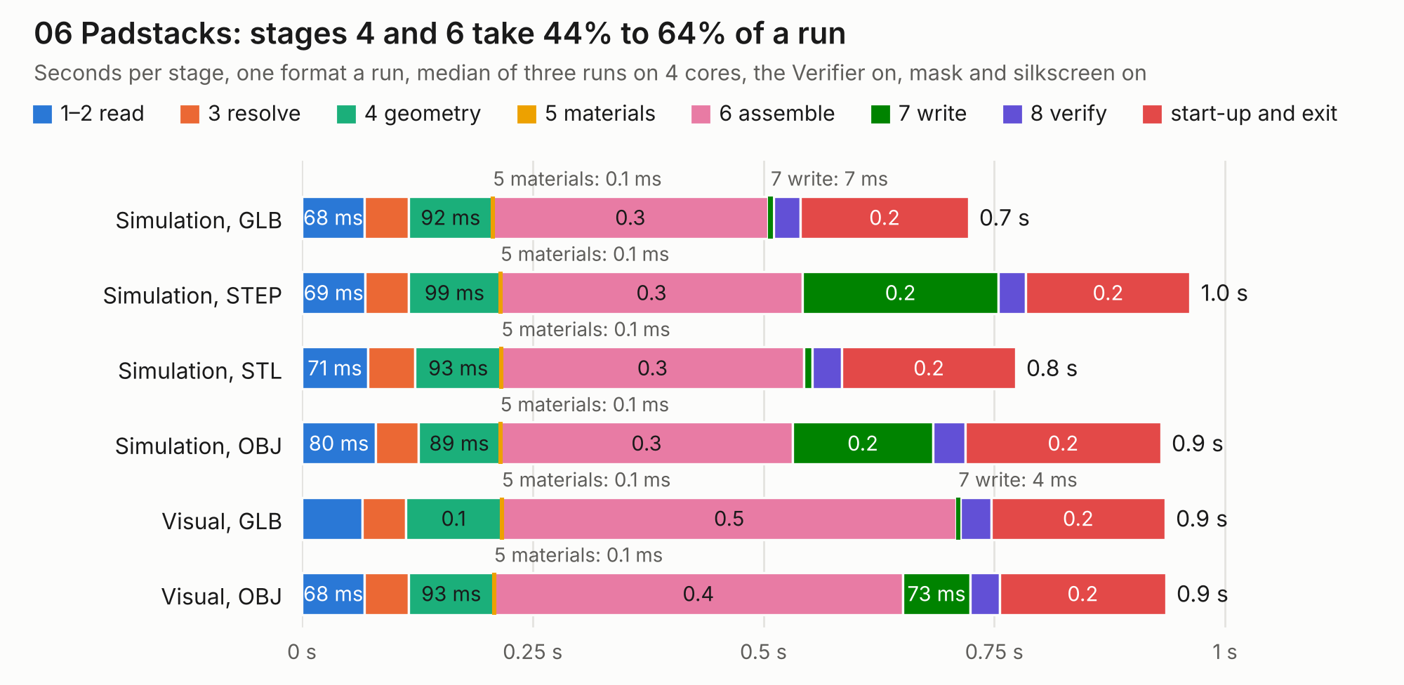
| Mode and format | 1–2 read | 3 resolve | 4 geometry | 5 materials | 6 assemble | 7 write | 8 verify | start-up and exit | Total |
|---|---|---|---|---|---|---|---|---|---|
| Simulation, GLB | 68 ms | 48 ms | 92 ms | 0.1 ms | 0.3 | 7 ms | 29 ms | 0.2 | 0.7 |
| Simulation, STEP | 69 ms | 47 ms | 99 ms | 0.1 ms | 0.3 | 0.2 | 30 ms | 0.2 | 1.0 |
| Simulation, STL | 71 ms | 51 ms | 93 ms | 0.1 ms | 0.3 | 9 ms | 32 ms | 0.2 | 0.8 |
| Simulation, OBJ | 80 ms | 46 ms | 89 ms | 0.1 ms | 0.3 | 0.2 | 35 ms | 0.2 | 0.9 |
| Visual, GLB | 65 ms | 47 ms | 0.1 | 0.1 ms | 0.5 | 4 ms | 33 ms | 0.2 | 0.9 |
| Visual, OBJ | 68 ms | 48 ms | 93 ms | 0.1 ms | 0.4 | 73 ms | 32 ms | 0.2 | 0.9 |
|
|
|||||||||||||||||||||||||||||||||||||||||
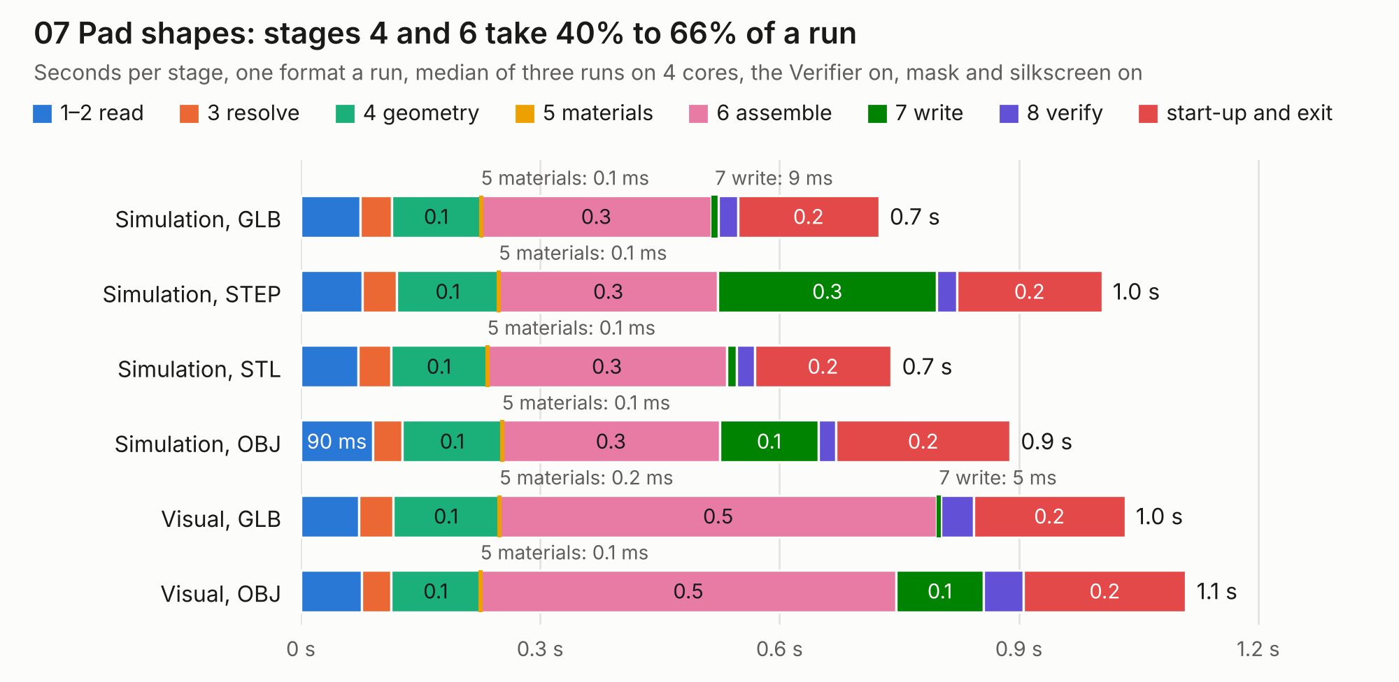
| Mode and format | 1–2 read | 3 resolve | 4 geometry | 5 materials | 6 assemble | 7 write | 8 verify | start-up and exit | Total |
|---|---|---|---|---|---|---|---|---|---|
| Simulation, GLB | 74 ms | 40 ms | 0.1 | 0.1 ms | 0.3 | 9 ms | 25 ms | 0.2 | 0.7 |
| Simulation, STEP | 77 ms | 44 ms | 0.1 | 0.1 ms | 0.3 | 0.3 | 25 ms | 0.2 | 1.0 |
| Simulation, STL | 72 ms | 41 ms | 0.1 | 0.1 ms | 0.3 | 12 ms | 23 ms | 0.2 | 0.7 |
| Simulation, OBJ | 90 ms | 37 ms | 0.1 | 0.1 ms | 0.3 | 0.1 | 22 ms | 0.2 | 0.9 |
| Visual, GLB | 73 ms | 43 ms | 0.1 | 0.2 ms | 0.5 | 5 ms | 41 ms | 0.2 | 1.0 |
| Visual, OBJ | 76 ms | 37 ms | 0.1 | 0.1 ms | 0.5 | 0.1 | 50 ms | 0.2 | 1.1 |
|
|
|||||||||||||||||||||||||||||||||||||||||
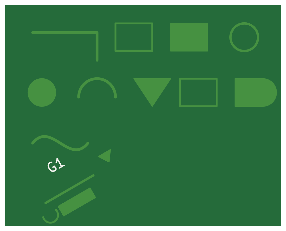
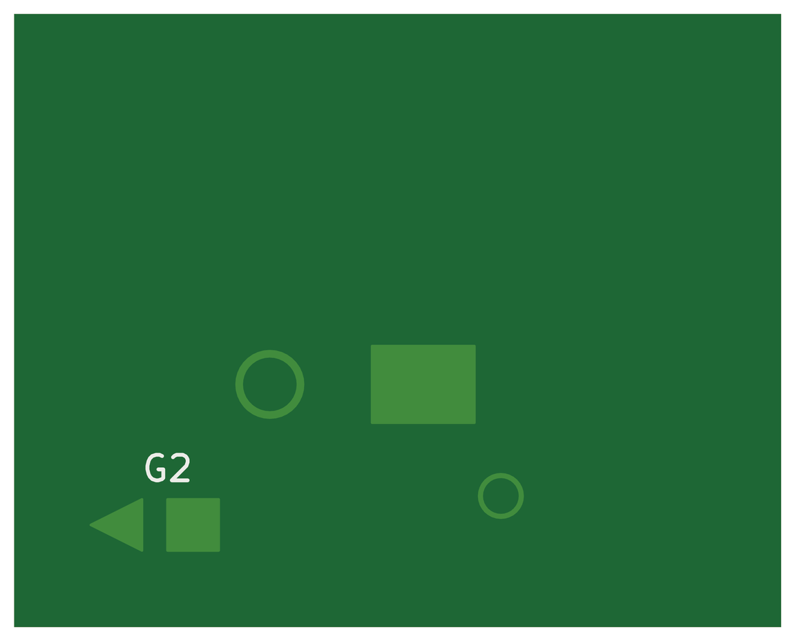
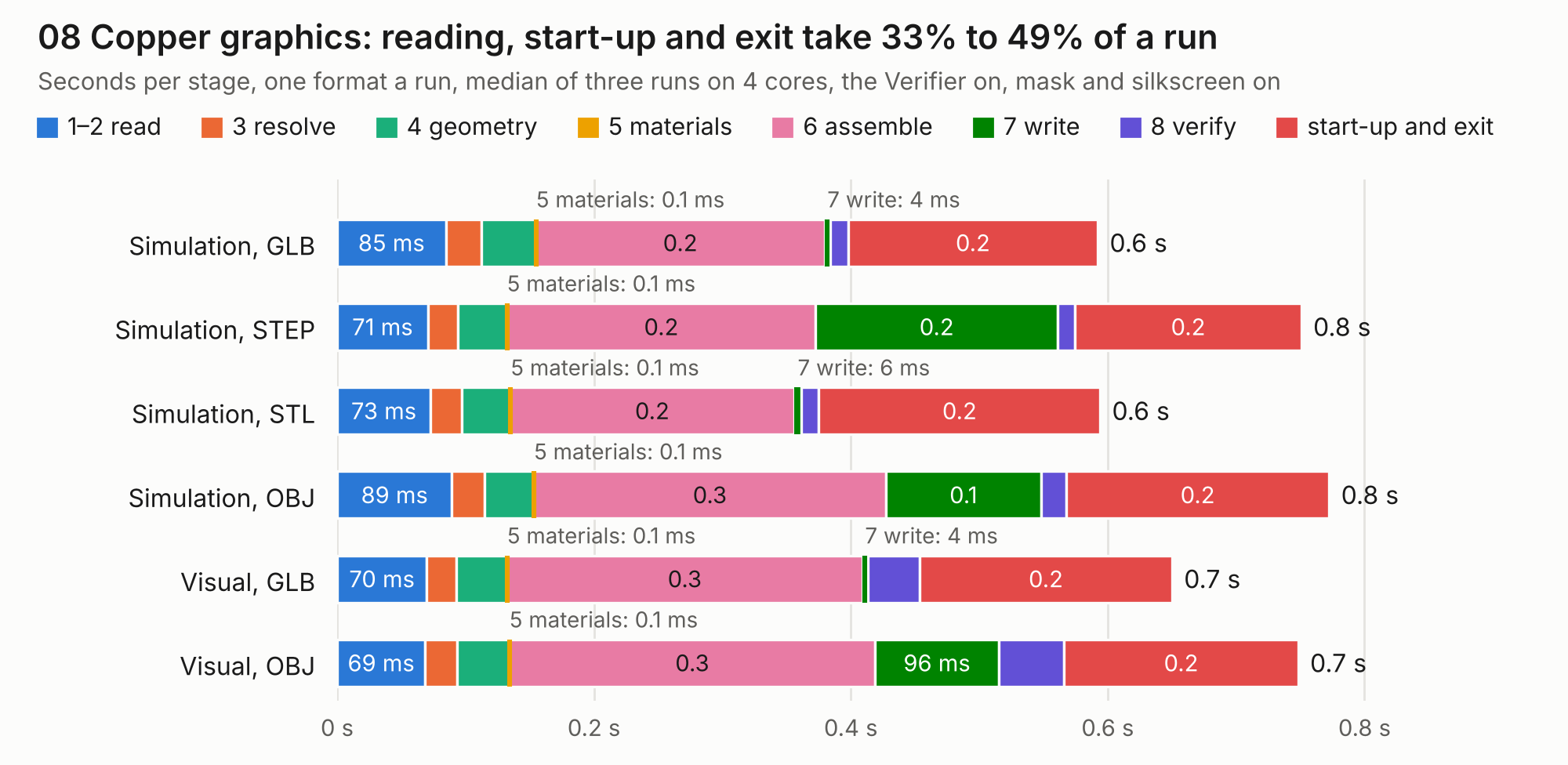
| Mode and format | 1–2 read | 3 resolve | 4 geometry | 5 materials | 6 assemble | 7 write | 8 verify | start-up and exit | Total |
|---|---|---|---|---|---|---|---|---|---|
| Simulation, GLB | 85 ms | 27 ms | 43 ms | 0.1 ms | 0.2 | 4 ms | 14 ms | 0.2 | 0.6 |
| Simulation, STEP | 71 ms | 23 ms | 38 ms | 0.1 ms | 0.2 | 0.2 | 13 ms | 0.2 | 0.8 |
| Simulation, STL | 73 ms | 24 ms | 38 ms | 0.1 ms | 0.2 | 6 ms | 13 ms | 0.2 | 0.6 |
| Simulation, OBJ | 89 ms | 25 ms | 39 ms | 0.1 ms | 0.3 | 0.1 | 19 ms | 0.2 | 0.8 |
| Visual, GLB | 70 ms | 23 ms | 39 ms | 0.1 ms | 0.3 | 4 ms | 40 ms | 0.2 | 0.7 |
| Visual, OBJ | 69 ms | 25 ms | 41 ms | 0.1 ms | 0.3 | 96 ms | 51 ms | 0.2 | 0.7 |
|
|
|||||||||||||||||||||||||||||||||||||||||
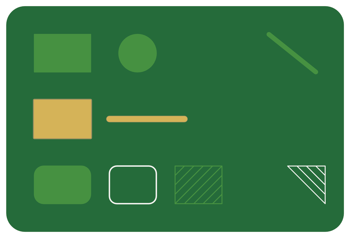
| Mode and format | 1–2 read | 3 resolve | 4 geometry | 5 materials | 6 assemble | 7 write | 8 verify | start-up and exit | Total |
|---|---|---|---|---|---|---|---|---|---|
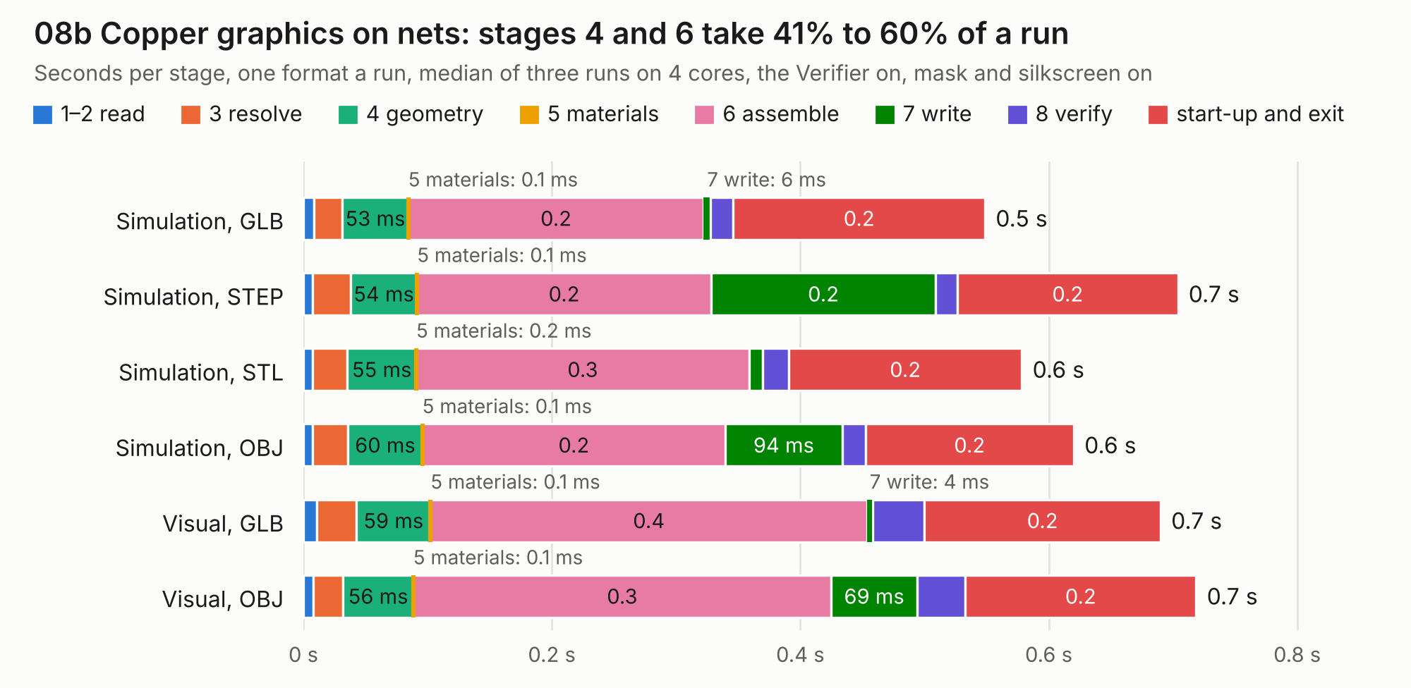
| Simulation, GLB | 8 ms | 23 ms | 53 ms | 0.1 ms | 0.2 | 6 ms | 18 ms | 0.2 | 0.5 |
| Simulation, STEP | 7 ms | 31 ms | 54 ms | 0.1 ms | 0.2 | 0.2 | 17 ms | 0.2 | 0.7 |
| Simulation, STL | 7 ms | 28 ms | 55 ms | 0.2 ms | 0.3 | 11 ms | 21 ms | 0.2 | 0.6 |
| Simulation, OBJ | 7 ms | 29 ms | 60 ms | 0.1 ms | 0.2 | 94 ms | 19 ms | 0.2 | 0.6 |
| Visual, GLB | 11 ms | 32 ms | 59 ms | 0.1 ms | 0.4 | 4 ms | 42 ms | 0.2 | 0.7 |
| Visual, OBJ | 8 ms | 24 ms | 56 ms | 0.1 ms | 0.3 | 69 ms | 38 ms | 0.2 | 0.7 |
|
|
|||||||||||||||||||||||||||||||||||||||||
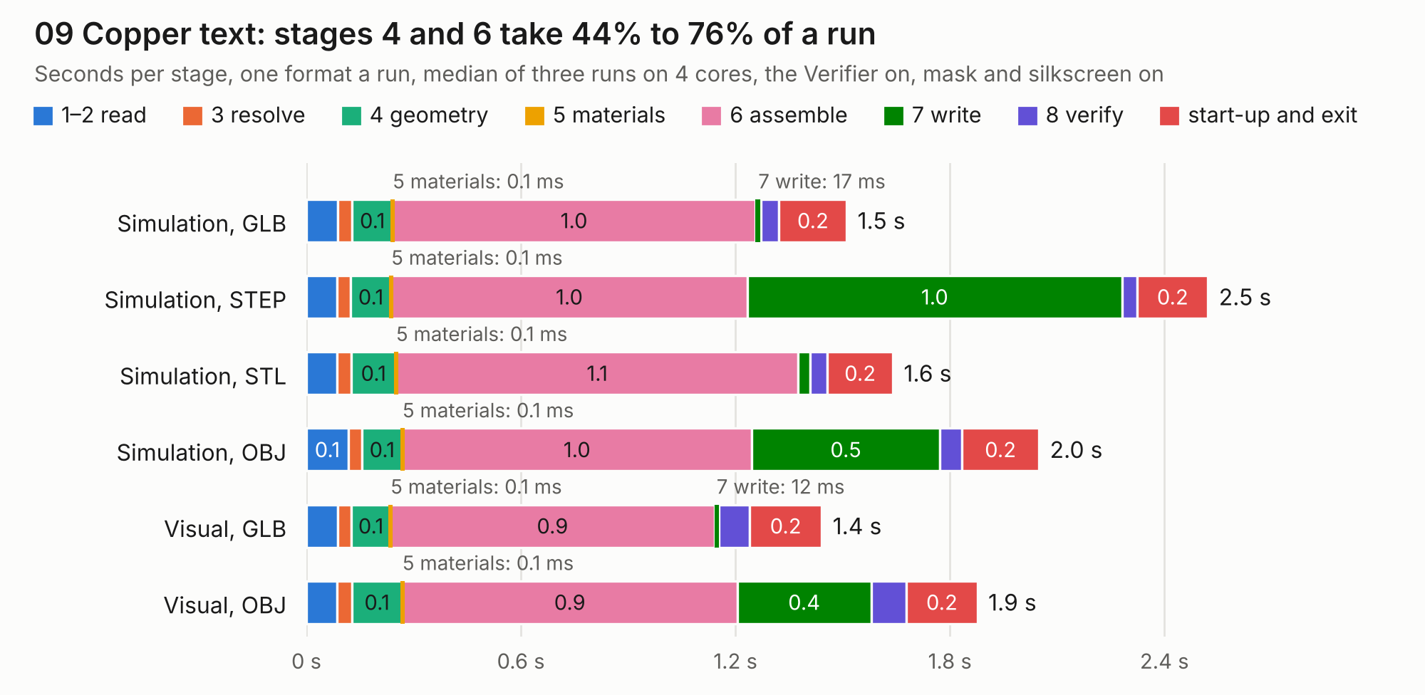
| Mode and format | 1–2 read | 3 resolve | 4 geometry | 5 materials | 6 assemble | 7 write | 8 verify | start-up and exit | Total |
|---|---|---|---|---|---|---|---|---|---|
| Simulation, GLB | 87 ms | 41 ms | 0.1 | 0.1 ms | 1.0 | 17 ms | 50 ms | 0.2 | 1.5 |
| Simulation, STEP | 85 ms | 38 ms | 0.1 | 0.1 ms | 1.0 | 1.0 | 42 ms | 0.2 | 2.5 |
| Simulation, STL | 87 ms | 38 ms | 0.1 | 0.1 ms | 1.1 | 34 ms | 47 ms | 0.2 | 1.6 |
| Simulation, OBJ | 0.1 | 38 ms | 0.1 | 0.1 ms | 1.0 | 0.5 | 61 ms | 0.2 | 2.0 |
| Visual, GLB | 88 ms | 38 ms | 0.1 | 0.1 ms | 0.9 | 12 ms | 86 ms | 0.2 | 1.4 |
| Visual, OBJ | 87 ms | 40 ms | 0.1 | 0.1 ms | 0.9 | 0.4 | 98 ms | 0.2 | 1.9 |
|
|
|||||||||||||||||||||||||||||||||||||||||

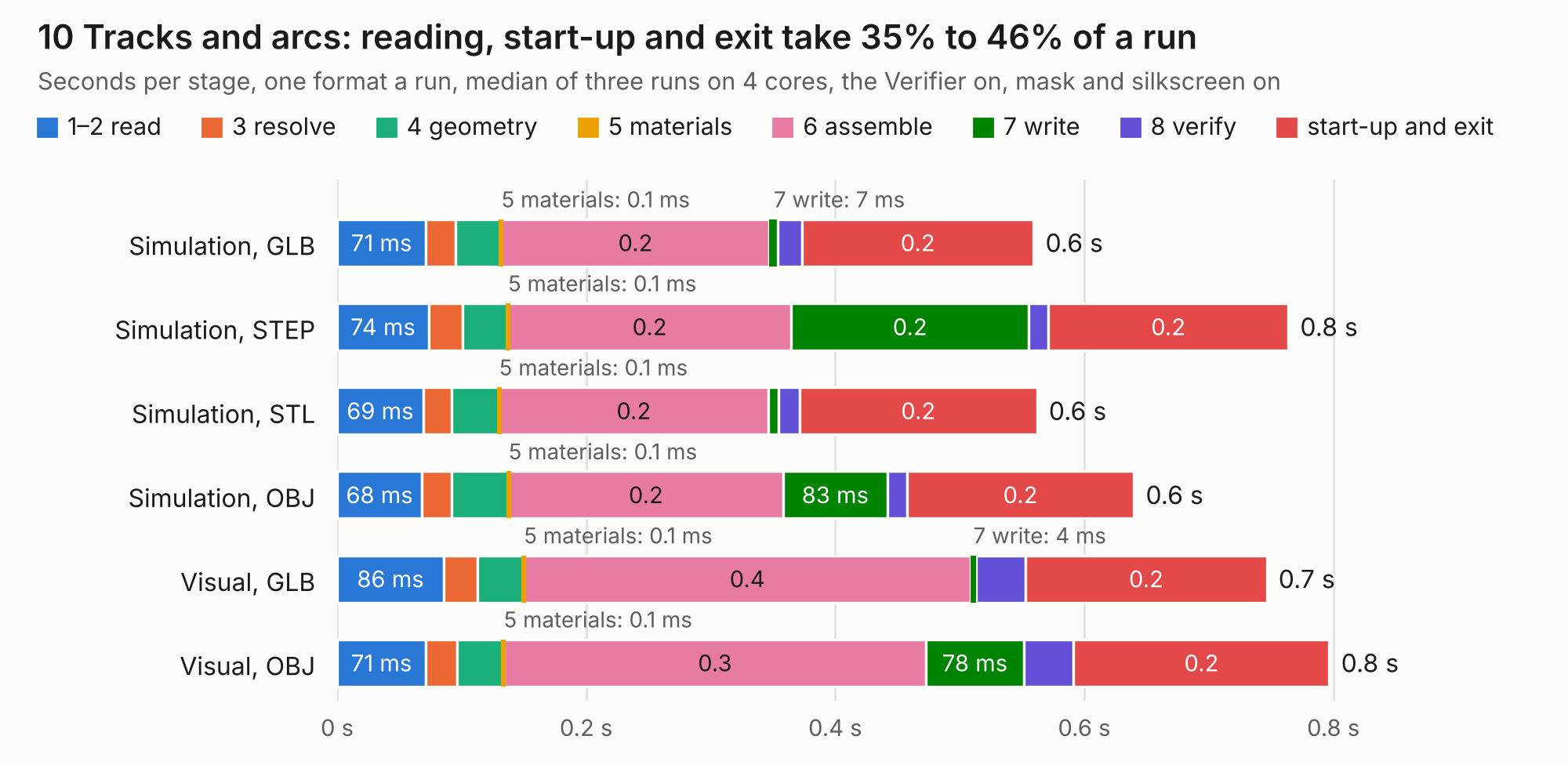
| Mode and format | 1–2 read | 3 resolve | 4 geometry | 5 materials | 6 assemble | 7 write | 8 verify | start-up and exit | Total |
|---|---|---|---|---|---|---|---|---|---|
| Simulation, GLB | 71 ms | 24 ms | 37 ms | 0.1 ms | 0.2 | 7 ms | 19 ms | 0.2 | 0.6 |
| Simulation, STEP | 74 ms | 27 ms | 36 ms | 0.1 ms | 0.2 | 0.2 | 16 ms | 0.2 | 0.8 |
| Simulation, STL | 69 ms | 23 ms | 38 ms | 0.1 ms | 0.2 | 8 ms | 17 ms | 0.2 | 0.6 |
| Simulation, OBJ | 68 ms | 24 ms | 46 ms | 0.1 ms | 0.2 | 83 ms | 16 ms | 0.2 | 0.6 |
| Visual, GLB | 86 ms | 27 ms | 37 ms | 0.1 ms | 0.4 | 4 ms | 40 ms | 0.2 | 0.7 |
| Visual, OBJ | 71 ms | 25 ms | 38 ms | 0.1 ms | 0.3 | 78 ms | 40 ms | 0.2 | 0.8 |
|
|
|||||||||||||||||||||||||||||||||||||||||
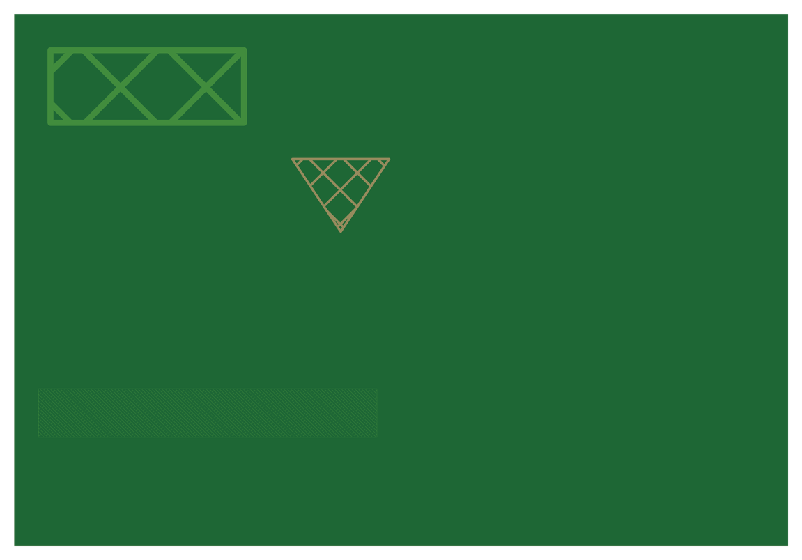
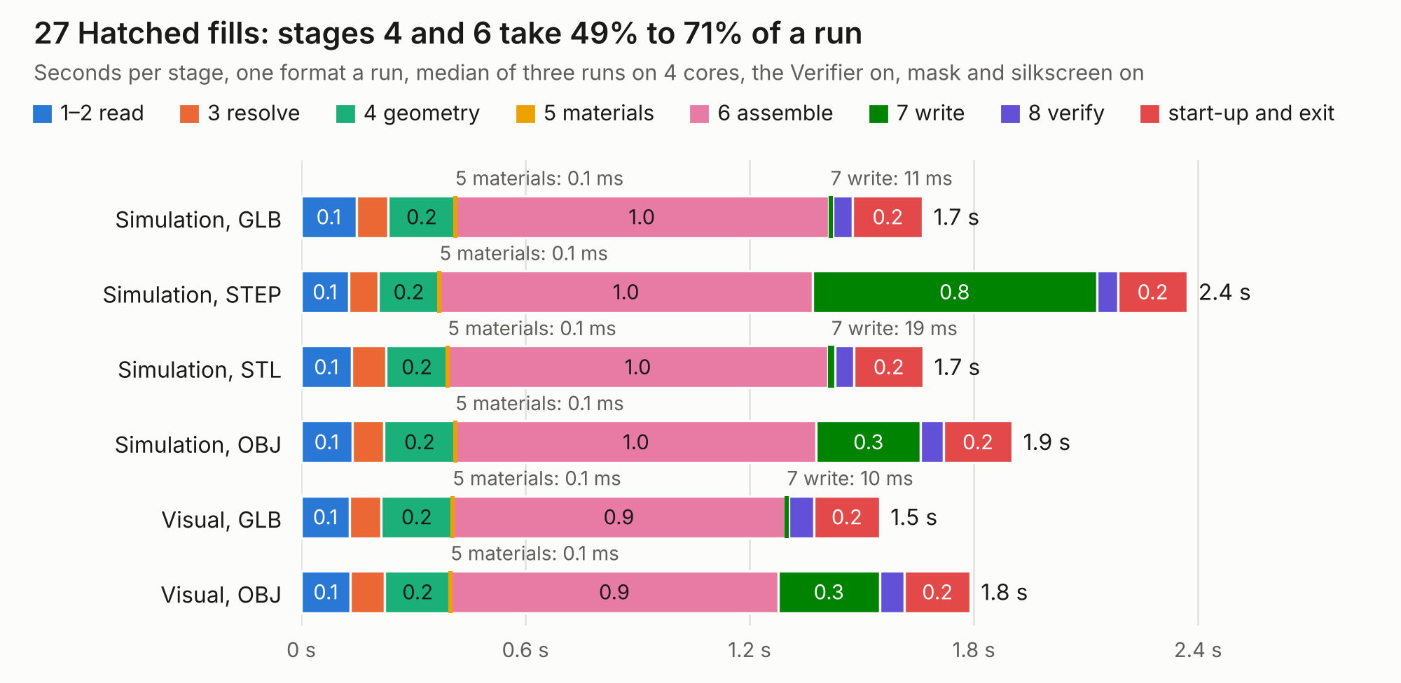
| Mode and format | 1–2 read | 3 resolve | 4 geometry | 5 materials | 6 assemble | 7 write | 8 verify | start-up and exit | Total |
|---|---|---|---|---|---|---|---|---|---|
| Simulation, GLB | 0.1 | 86 ms | 0.2 | 0.1 ms | 1.0 | 11 ms | 54 ms | 0.2 | 1.7 |
| Simulation, STEP | 0.1 | 78 ms | 0.2 | 0.1 ms | 1.0 | 0.8 | 56 ms | 0.2 | 2.4 |
| Simulation, STL | 0.1 | 92 ms | 0.2 | 0.1 ms | 1.0 | 19 ms | 51 ms | 0.2 | 1.7 |
| Simulation, OBJ | 0.1 | 85 ms | 0.2 | 0.1 ms | 1.0 | 0.3 | 61 ms | 0.2 | 1.9 |
| Visual, GLB | 0.1 | 84 ms | 0.2 | 0.1 ms | 0.9 | 10 ms | 67 ms | 0.2 | 1.5 |
| Visual, OBJ | 0.1 | 92 ms | 0.2 | 0.1 ms | 0.9 | 0.3 | 66 ms | 0.2 | 1.8 |
|
|
|||||||||||||||||||||||||||||||||||||||||
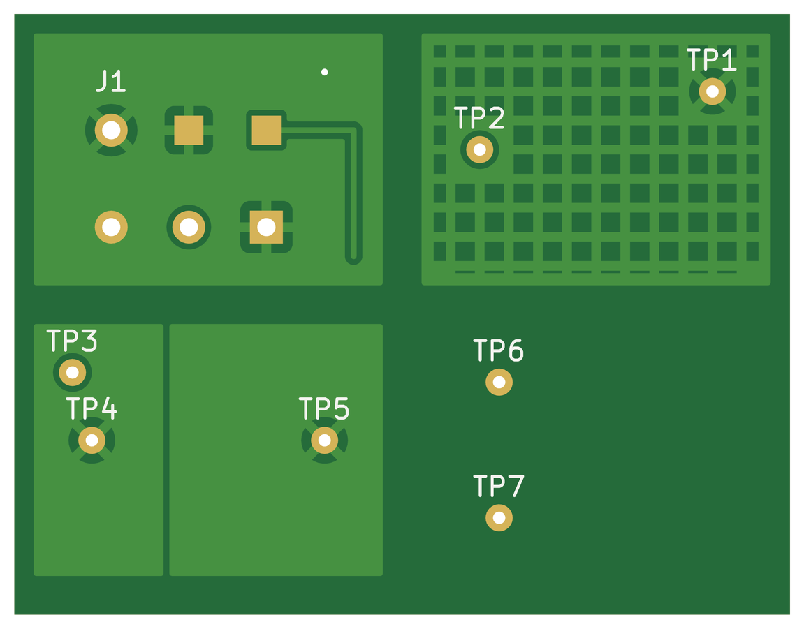
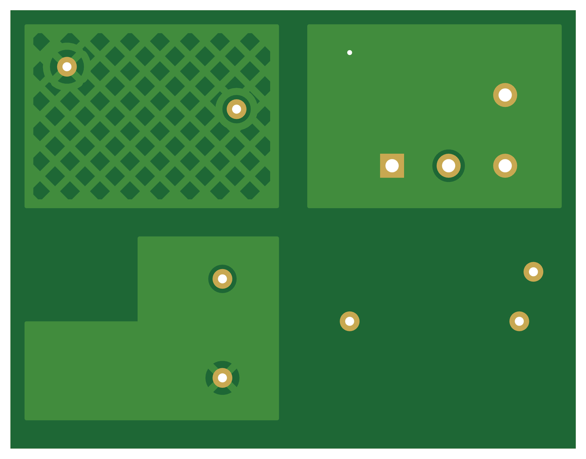
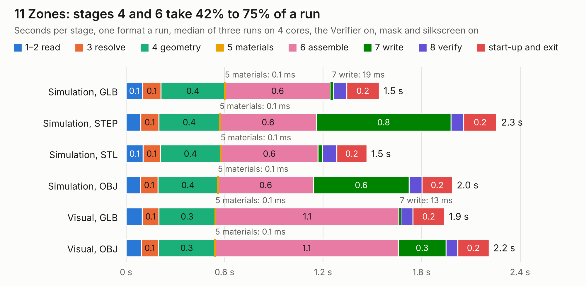
| Mode and format | 1–2 read | 3 resolve | 4 geometry | 5 materials | 6 assemble | 7 write | 8 verify | start-up and exit | Total |
|---|---|---|---|---|---|---|---|---|---|
| Simulation, GLB | 0.1 | 0.1 | 0.4 | 0.1 ms | 0.6 | 19 ms | 80 ms | 0.2 | 1.5 |
| Simulation, STEP | 89 ms | 0.1 | 0.4 | 0.1 ms | 0.6 | 0.8 | 77 ms | 0.2 | 2.3 |
| Simulation, STL | 0.1 | 0.1 | 0.4 | 0.1 ms | 0.6 | 26 ms | 88 ms | 0.2 | 1.5 |
| Simulation, OBJ | 87 ms | 0.1 | 0.4 | 0.1 ms | 0.6 | 0.6 | 80 ms | 0.2 | 2.0 |
| Visual, GLB | 99 ms | 0.1 | 0.3 | 0.1 ms | 1.1 | 13 ms | 72 ms | 0.2 | 1.9 |
| Visual, OBJ | 92 ms | 0.1 | 0.3 | 0.1 ms | 1.1 | 0.3 | 71 ms | 0.2 | 2.2 |
|
|
|||||||||||||||||||||||||||||||||||||||||
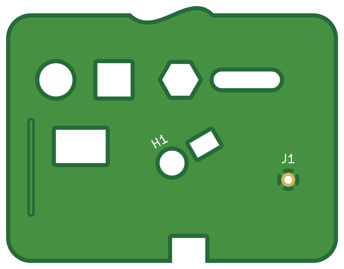
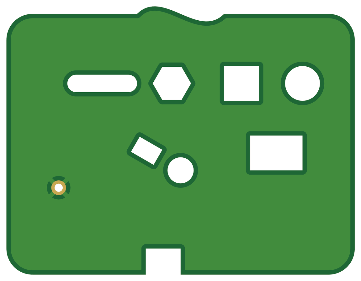
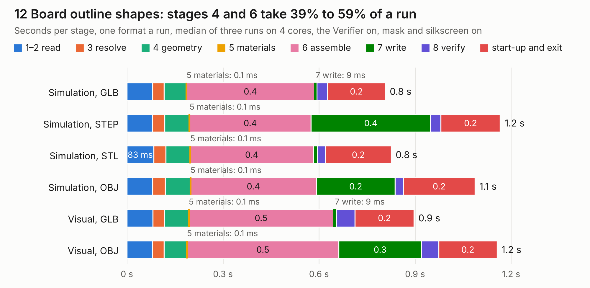
| Mode and format | 1–2 read | 3 resolve | 4 geometry | 5 materials | 6 assemble | 7 write | 8 verify | start-up and exit | Total |
|---|---|---|---|---|---|---|---|---|---|
| Simulation, GLB | 80 ms | 36 ms | 70 ms | 0.1 ms | 0.4 | 9 ms | 33 ms | 0.2 | 0.8 |
| Simulation, STEP | 79 ms | 39 ms | 77 ms | 0.1 ms | 0.4 | 0.4 | 32 ms | 0.2 | 1.2 |
| Simulation, STL | 83 ms | 38 ms | 77 ms | 0.1 ms | 0.4 | 13 ms | 26 ms | 0.2 | 0.8 |
| Simulation, OBJ | 80 ms | 40 ms | 79 ms | 0.1 ms | 0.4 | 0.2 | 26 ms | 0.2 | 1.1 |
| Visual, GLB | 81 ms | 37 ms | 76 ms | 0.1 ms | 0.5 | 9 ms | 58 ms | 0.2 | 0.9 |
| Visual, OBJ | 80 ms | 37 ms | 71 ms | 0.1 ms | 0.5 | 0.3 | 54 ms | 0.2 | 1.2 |
|
|
|||||||||||||||||||||||||||||||||||||||||
| Mode and format | 1–2 read | 3 resolve | 4 geometry | 5 materials | 6 assemble | 7 write | 8 verify | start-up and exit | Total |
|---|---|---|---|---|---|---|---|---|---|
| Simulation, GLB | 67 ms | 27 ms | 53 ms | 0.1 ms | 0.1 | 4 ms | 15 ms | 0.2 | 0.5 |
| Simulation, STEP | 70 ms | 26 ms | 55 ms | 0.1 ms | 0.1 | 0.1 | 18 ms | 0.2 | 0.6 |
| Simulation, STL | 67 ms | 25 ms | 55 ms | 0.1 ms | 0.1 | 6 ms | 17 ms | 0.2 | 0.5 |
| Simulation, OBJ | 65 ms | 23 ms | 53 ms | 0.1 ms | 0.1 | 62 ms | 16 ms | 0.2 | 0.6 |
| Visual, GLB | 71 ms | 24 ms | 54 ms | 0.1 ms | 0.2 | 4 ms | 64 ms | 0.2 | 0.6 |
| Visual, OBJ | 65 ms | 24 ms | 51 ms | 0.1 ms | 0.2 | 38 ms | 45 ms | 0.2 | 0.6 |
|
|
|||||||||||||||||||||||||||||||||||||||||

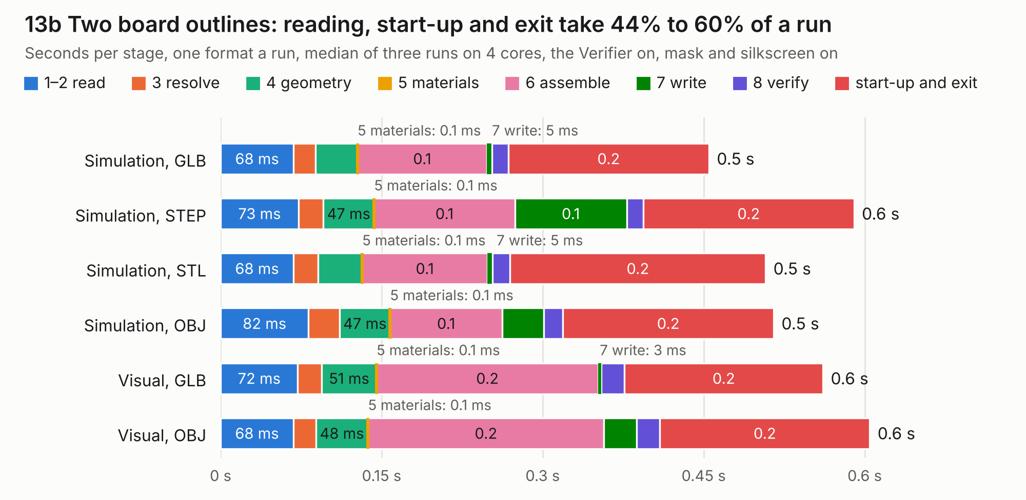
| Mode and format | 1–2 read | 3 resolve | 4 geometry | 5 materials | 6 assemble | 7 write | 8 verify | start-up and exit | Total |
|---|---|---|---|---|---|---|---|---|---|
| Simulation, GLB | 68 ms | 21 ms | 39 ms | 0.1 ms | 0.1 | 5 ms | 15 ms | 0.2 | 0.5 |
| Simulation, STEP | 73 ms | 23 ms | 47 ms | 0.1 ms | 0.1 | 0.1 | 15 ms | 0.2 | 0.6 |
| Simulation, STL | 68 ms | 23 ms | 41 ms | 0.1 ms | 0.1 | 5 ms | 16 ms | 0.2 | 0.5 |
| Simulation, OBJ | 82 ms | 29 ms | 47 ms | 0.1 ms | 0.1 | 39 ms | 18 ms | 0.2 | 0.5 |
| Visual, GLB | 72 ms | 22 ms | 51 ms | 0.1 ms | 0.2 | 3 ms | 22 ms | 0.2 | 0.6 |
| Visual, OBJ | 68 ms | 21 ms | 48 ms | 0.1 ms | 0.2 | 30 ms | 22 ms | 0.2 | 0.6 |
|
|
|||||||||||||||||||||||||||||||||||||||||

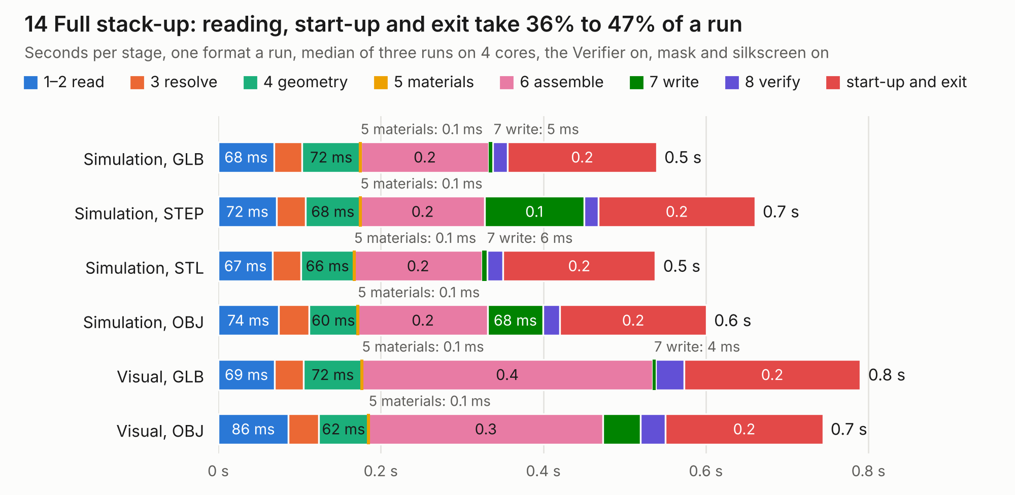
| Mode and format | 1–2 read | 3 resolve | 4 geometry | 5 materials | 6 assemble | 7 write | 8 verify | start-up and exit | Total |
|---|---|---|---|---|---|---|---|---|---|
| Simulation, GLB | 68 ms | 35 ms | 72 ms | 0.1 ms | 0.2 | 5 ms | 18 ms | 0.2 | 0.5 |
| Simulation, STEP | 72 ms | 36 ms | 68 ms | 0.1 ms | 0.2 | 0.1 | 18 ms | 0.2 | 0.7 |
| Simulation, STL | 67 ms | 35 ms | 66 ms | 0.1 ms | 0.2 | 6 ms | 20 ms | 0.2 | 0.5 |
| Simulation, OBJ | 74 ms | 38 ms | 60 ms | 0.1 ms | 0.2 | 68 ms | 21 ms | 0.2 | 0.6 |
| Visual, GLB | 69 ms | 36 ms | 72 ms | 0.1 ms | 0.4 | 4 ms | 35 ms | 0.2 | 0.8 |
| Visual, OBJ | 86 ms | 37 ms | 62 ms | 0.1 ms | 0.3 | 46 ms | 31 ms | 0.2 | 0.7 |
|
|
|||||||||||||||||||||||||||||||||||||||||


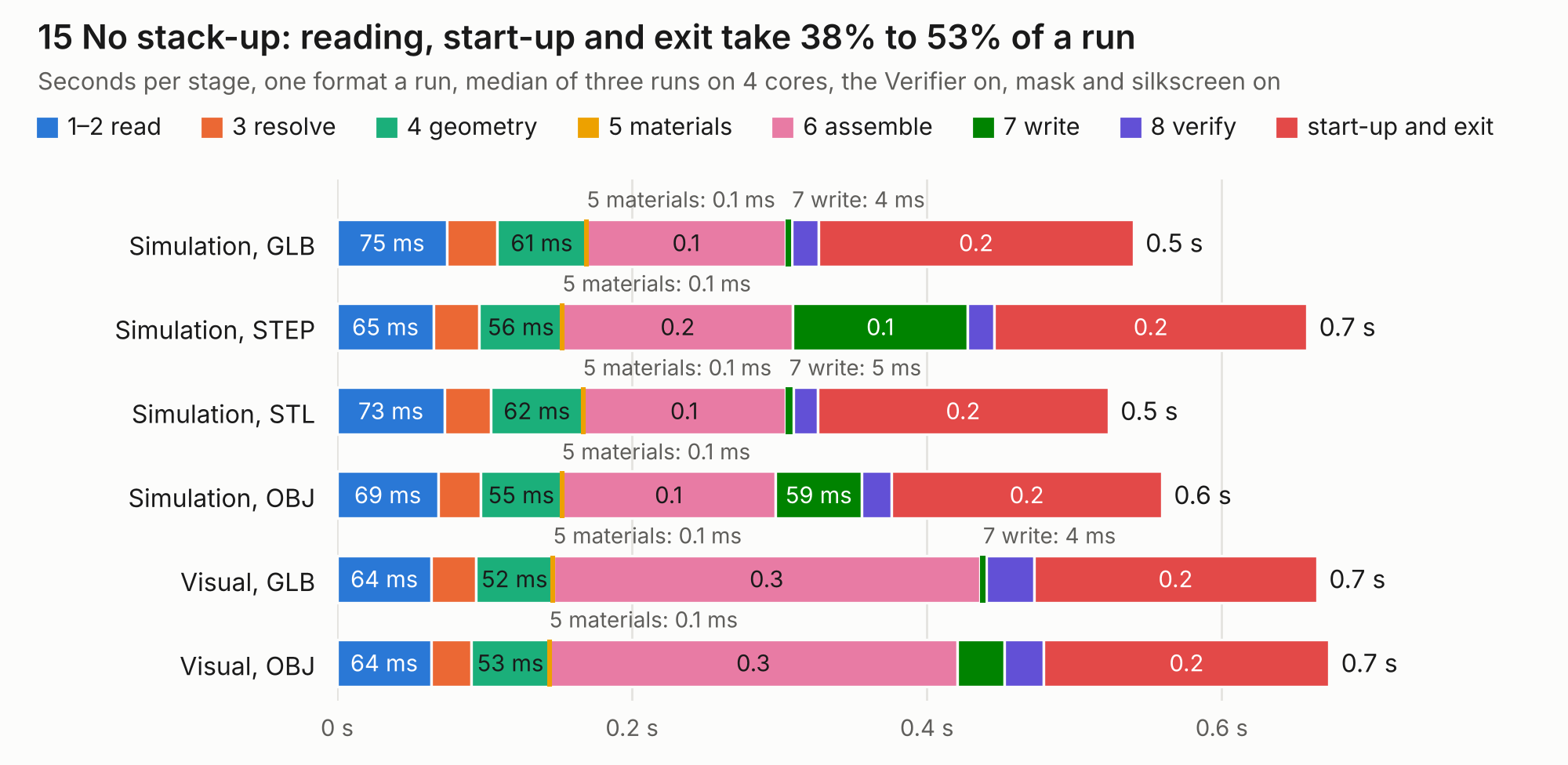
| Mode and format | 1–2 read | 3 resolve | 4 geometry | 5 materials | 6 assemble | 7 write | 8 verify | start-up and exit | Total |
|---|---|---|---|---|---|---|---|---|---|
| Simulation, GLB | 75 ms | 34 ms | 61 ms | 0.1 ms | 0.1 | 4 ms | 18 ms | 0.2 | 0.5 |
| Simulation, STEP | 65 ms | 31 ms | 56 ms | 0.1 ms | 0.2 | 0.1 | 18 ms | 0.2 | 0.7 |
| Simulation, STL | 73 ms | 31 ms | 62 ms | 0.1 ms | 0.1 | 5 ms | 17 ms | 0.2 | 0.5 |
| Simulation, OBJ | 69 ms | 29 ms | 55 ms | 0.1 ms | 0.1 | 59 ms | 20 ms | 0.2 | 0.6 |
| Visual, GLB | 64 ms | 30 ms | 52 ms | 0.1 ms | 0.3 | 4 ms | 32 ms | 0.2 | 0.7 |
| Visual, OBJ | 64 ms | 27 ms | 53 ms | 0.1 ms | 0.3 | 32 ms | 27 ms | 0.2 | 0.7 |
|
|
|||||||||||||||||||||||||||||||||||||||||
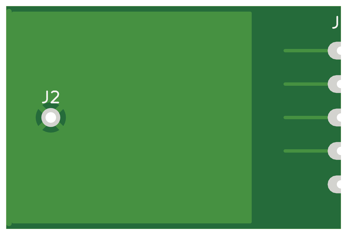
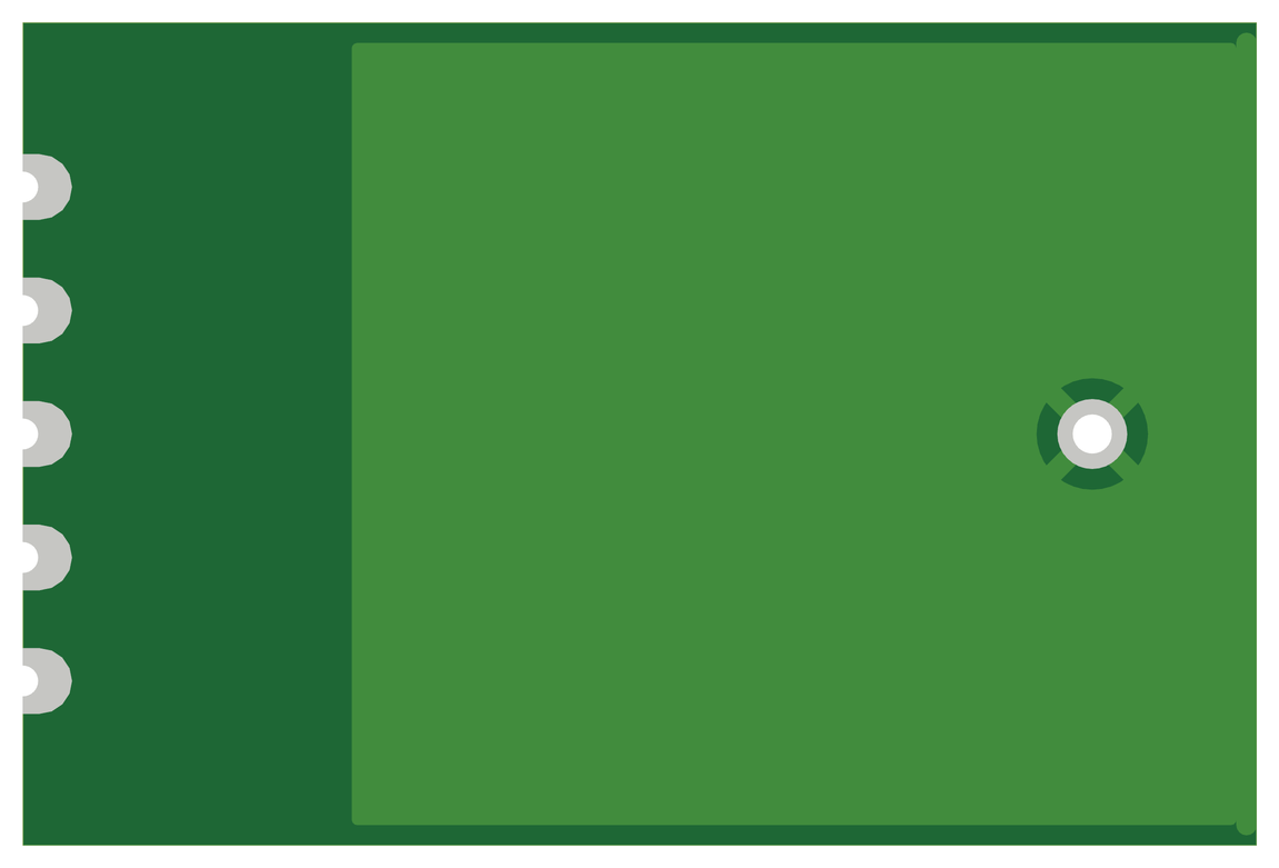
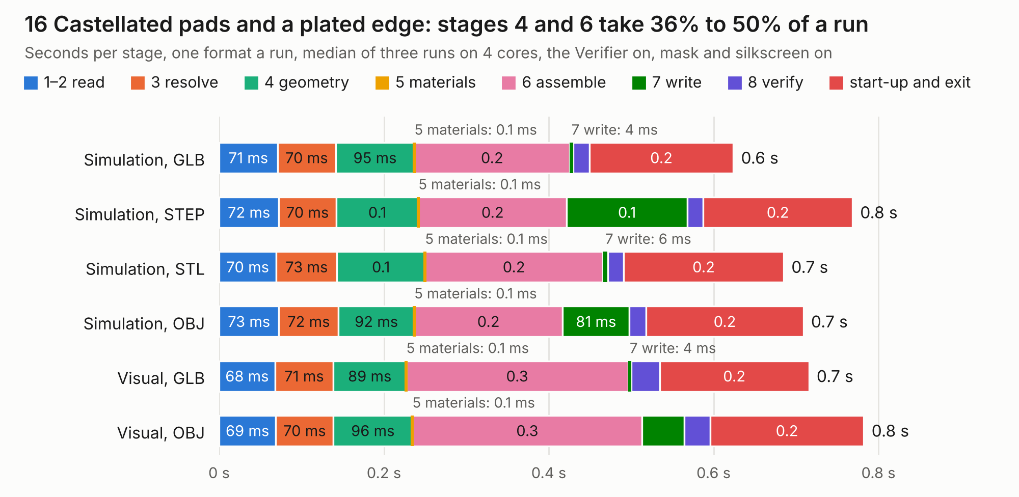
| Mode and format | 1–2 read | 3 resolve | 4 geometry | 5 materials | 6 assemble | 7 write | 8 verify | start-up and exit | Total |
|---|---|---|---|---|---|---|---|---|---|
| Simulation, GLB | 71 ms | 70 ms | 95 ms | 0.1 ms | 0.2 | 4 ms | 20 ms | 0.2 | 0.6 |
| Simulation, STEP | 72 ms | 70 ms | 0.1 | 0.1 ms | 0.2 | 0.1 | 19 ms | 0.2 | 0.8 |
| Simulation, STL | 70 ms | 73 ms | 0.1 | 0.1 ms | 0.2 | 6 ms | 19 ms | 0.2 | 0.7 |
| Simulation, OBJ | 73 ms | 72 ms | 92 ms | 0.1 ms | 0.2 | 81 ms | 20 ms | 0.2 | 0.7 |
| Visual, GLB | 68 ms | 71 ms | 89 ms | 0.1 ms | 0.3 | 4 ms | 34 ms | 0.2 | 0.7 |
| Visual, OBJ | 69 ms | 70 ms | 96 ms | 0.1 ms | 0.3 | 51 ms | 31 ms | 0.2 | 0.8 |
|
|
|||||||||||||||||||||||||||||||||||||||||
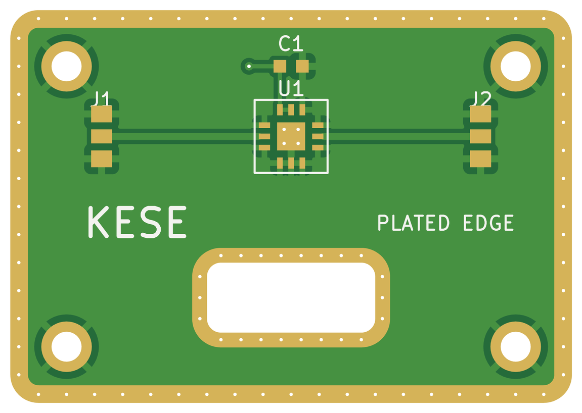
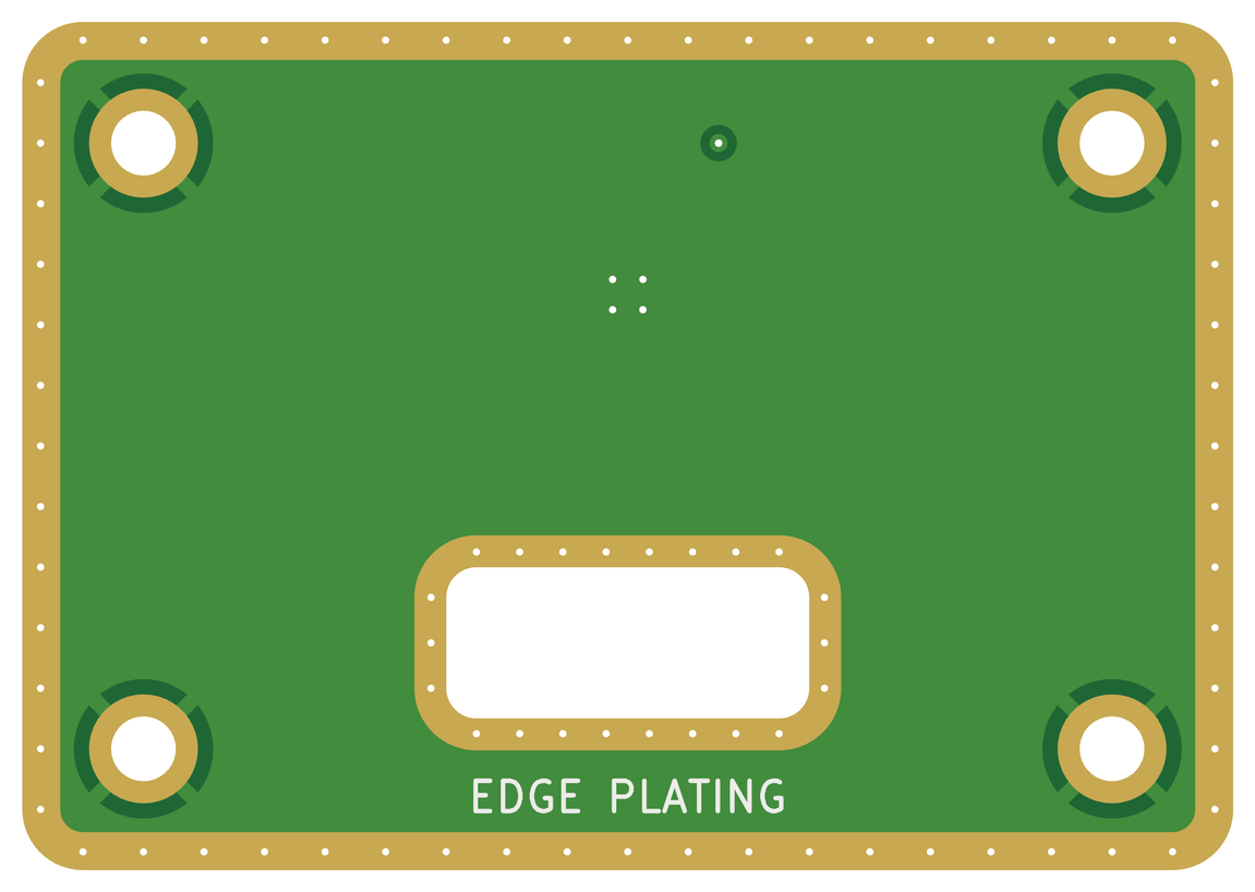
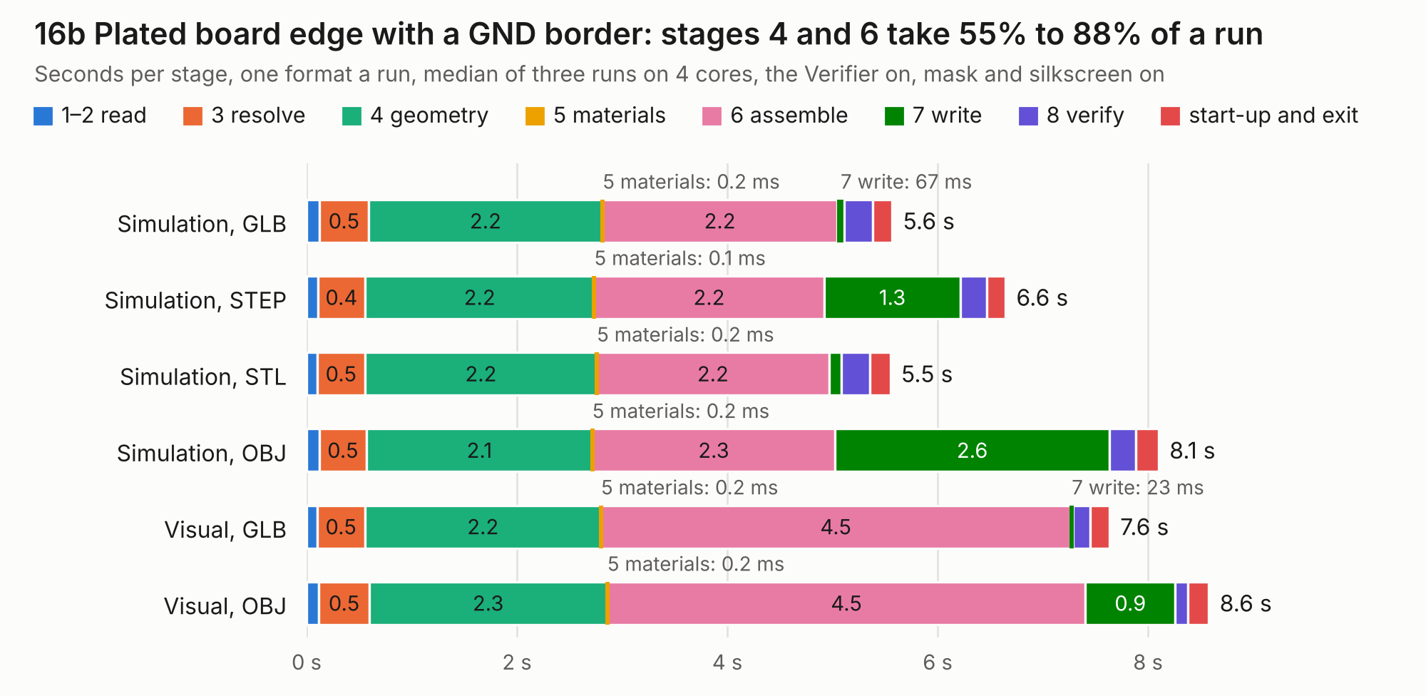
| Mode and format | 1–2 read | 3 resolve | 4 geometry | 5 materials | 6 assemble | 7 write | 8 verify | start-up and exit | Total |
|---|---|---|---|---|---|---|---|---|---|
| Simulation, GLB | 0.1 | 0.5 | 2.2 | 0.2 ms | 2.2 | 67 ms | 0.3 | 0.2 | 5.6 |
| Simulation, STEP | 0.1 | 0.4 | 2.2 | 0.1 ms | 2.2 | 1.3 | 0.2 | 0.2 | 6.6 |
| Simulation, STL | 0.1 | 0.5 | 2.2 | 0.2 ms | 2.2 | 0.1 | 0.3 | 0.2 | 5.5 |
| Simulation, OBJ | 0.1 | 0.5 | 2.1 | 0.2 ms | 2.3 | 2.6 | 0.3 | 0.2 | 8.1 |
| Visual, GLB | 99 ms | 0.5 | 2.2 | 0.2 ms | 4.5 | 23 ms | 0.2 | 0.2 | 7.6 |
| Visual, OBJ | 0.1 | 0.5 | 2.3 | 0.2 ms | 4.5 | 0.9 | 0.1 | 0.2 | 8.6 |
|
|
|||||||||||||||||||||||||||||||||||||||||
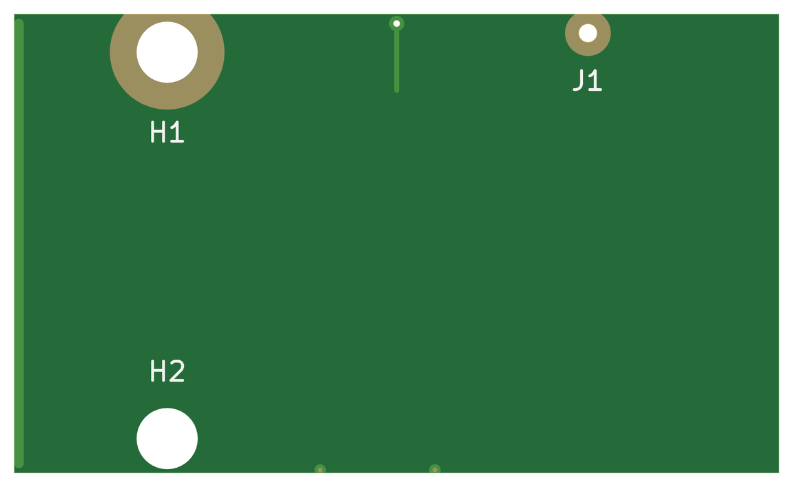
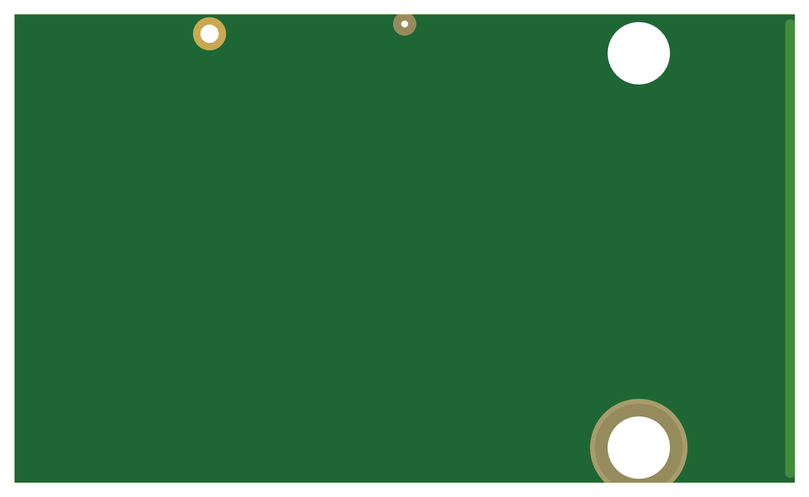
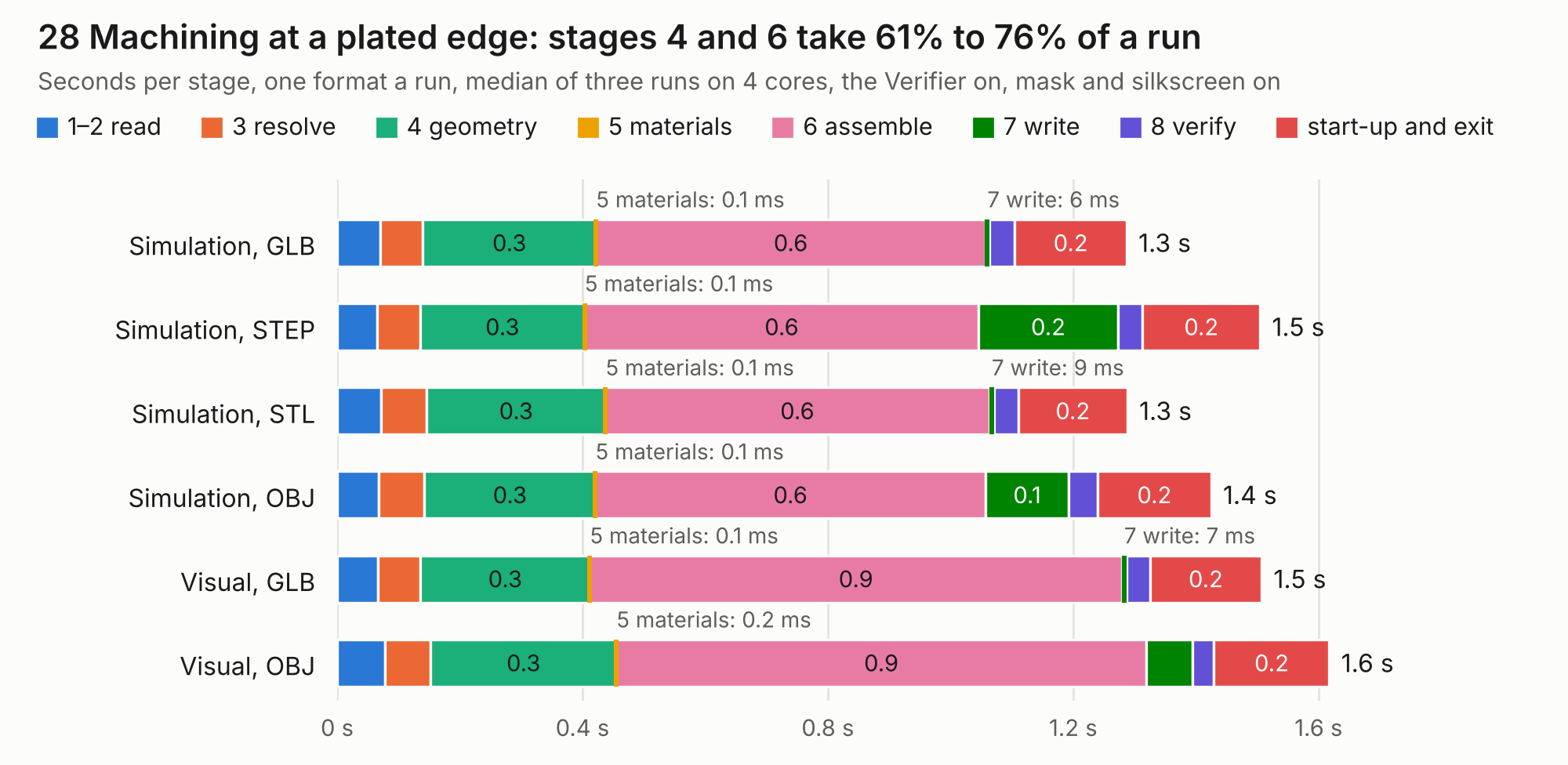
| Mode and format | 1–2 read | 3 resolve | 4 geometry | 5 materials | 6 assemble | 7 write | 8 verify | start-up and exit | Total |
|---|---|---|---|---|---|---|---|---|---|
| Simulation, GLB | 70 ms | 69 ms | 0.3 | 0.1 ms | 0.6 | 6 ms | 42 ms | 0.2 | 1.3 |
| Simulation, STEP | 66 ms | 70 ms | 0.3 | 0.1 ms | 0.6 | 0.2 | 40 ms | 0.2 | 1.5 |
| Simulation, STL | 72 ms | 75 ms | 0.3 | 0.1 ms | 0.6 | 9 ms | 39 ms | 0.2 | 1.3 |
| Simulation, OBJ | 68 ms | 74 ms | 0.3 | 0.1 ms | 0.6 | 0.1 | 47 ms | 0.2 | 1.4 |
| Visual, GLB | 67 ms | 69 ms | 0.3 | 0.1 ms | 0.9 | 7 ms | 38 ms | 0.2 | 1.5 |
| Visual, OBJ | 78 ms | 75 ms | 0.3 | 0.2 ms | 0.9 | 76 ms | 35 ms | 0.2 | 1.6 |
|
|
|||||||||||||||||||||||||||||||||||||||||
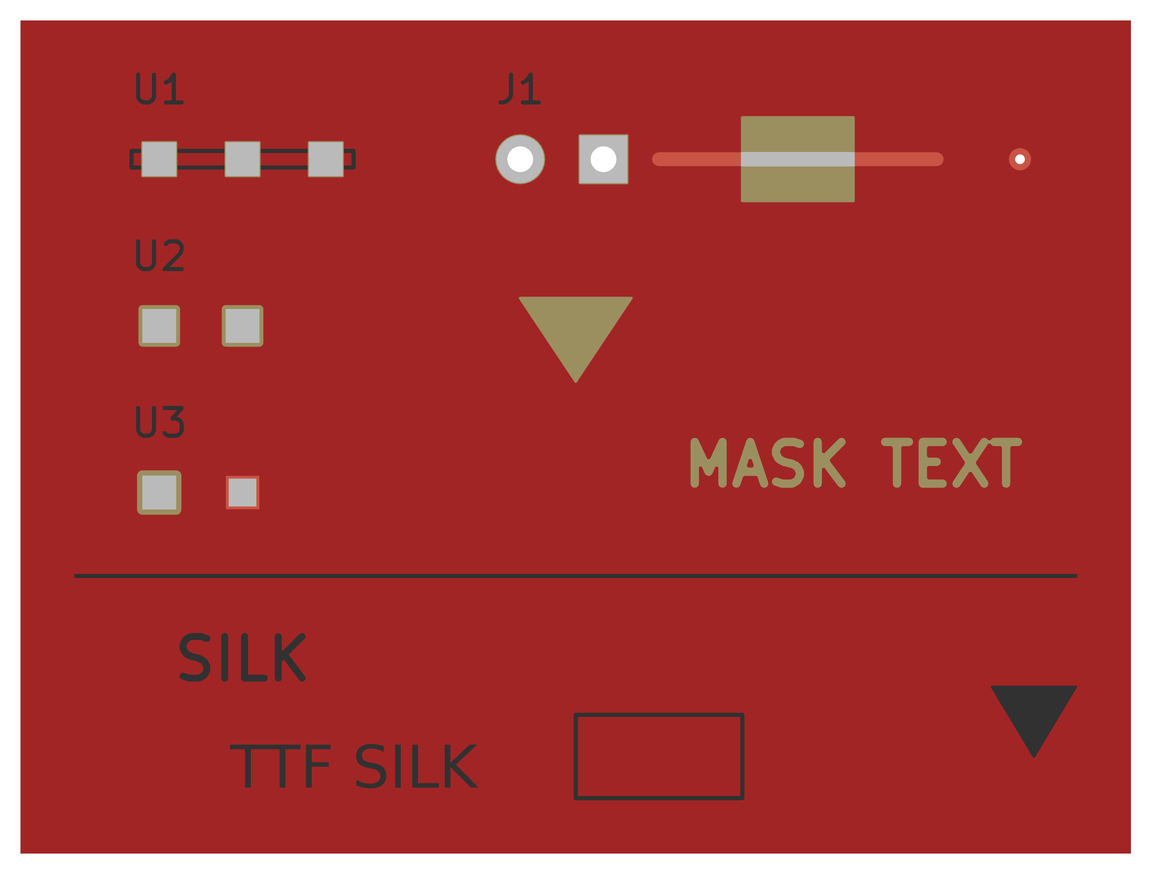
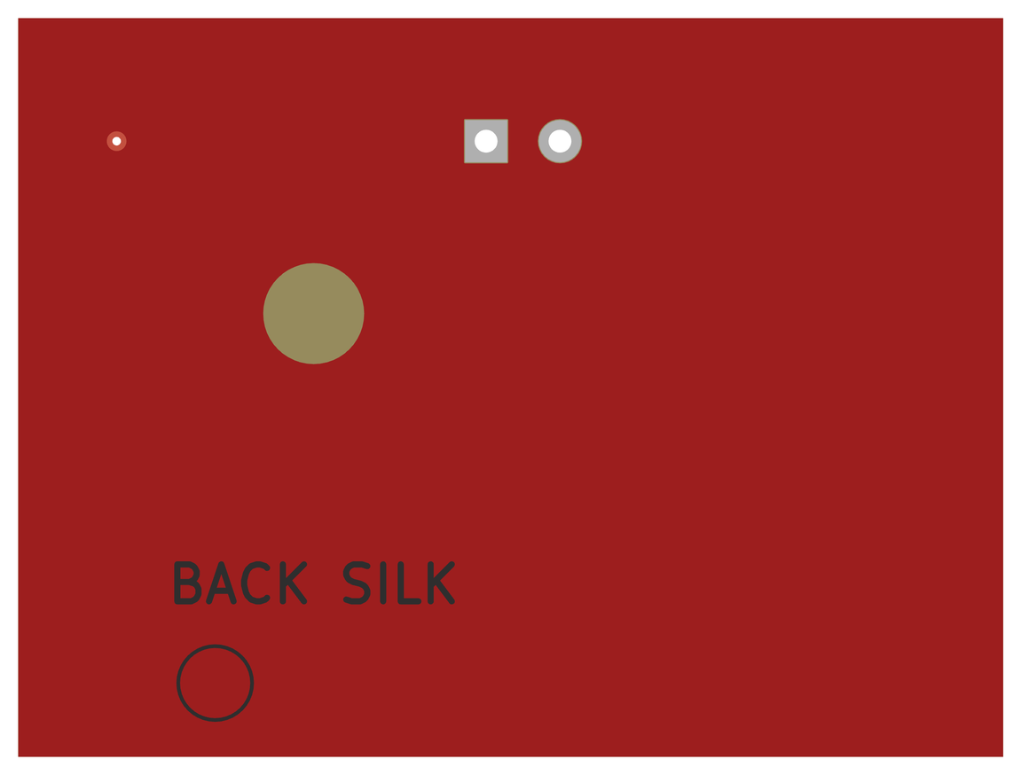
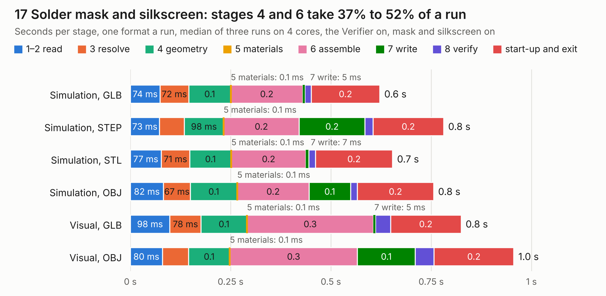
| Mode and format | 1–2 read | 3 resolve | 4 geometry | 5 materials | 6 assemble | 7 write | 8 verify | start-up and exit | Total |
|---|---|---|---|---|---|---|---|---|---|
| Simulation, GLB | 74 ms | 72 ms | 0.1 | 0.1 ms | 0.2 | 5 ms | 16 ms | 0.2 | 0.6 |
| Simulation, STEP | 73 ms | 62 ms | 98 ms | 0.1 ms | 0.2 | 0.2 | 20 ms | 0.2 | 0.8 |
| Simulation, STL | 77 ms | 71 ms | 0.1 | 0.1 ms | 0.2 | 7 ms | 17 ms | 0.2 | 0.7 |
| Simulation, OBJ | 82 ms | 67 ms | 0.1 | 0.1 ms | 0.2 | 0.1 | 17 ms | 0.2 | 0.8 |
| Visual, GLB | 98 ms | 78 ms | 0.1 | 0.1 ms | 0.3 | 5 ms | 38 ms | 0.2 | 0.8 |
| Visual, OBJ | 80 ms | 65 ms | 0.1 | 0.1 ms | 0.3 | 0.1 | 47 ms | 0.2 | 1.0 |
|
|
|||||||||||||||||||||||||||||||||||||||||
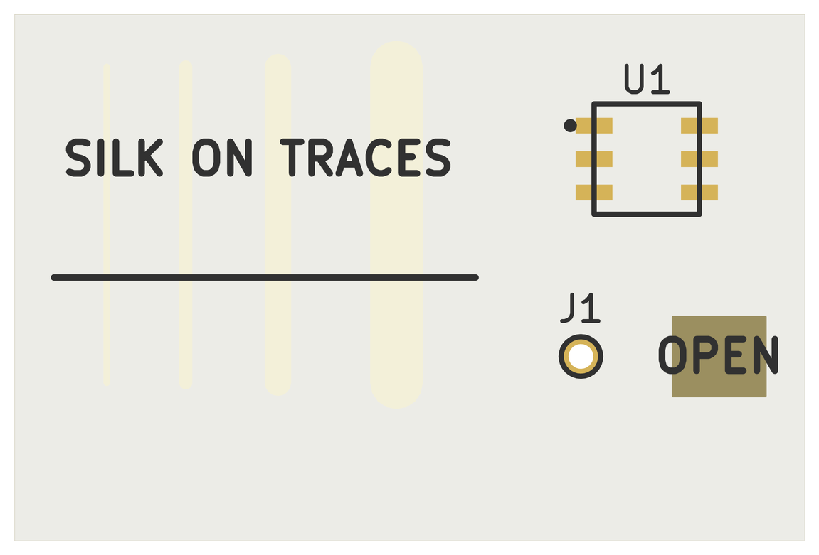
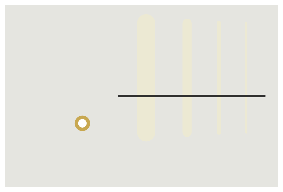
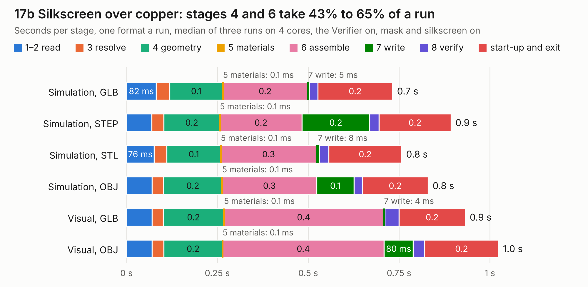
| Mode and format | 1–2 read | 3 resolve | 4 geometry | 5 materials | 6 assemble | 7 write | 8 verify | start-up and exit | Total |
|---|---|---|---|---|---|---|---|---|---|
| Simulation, GLB | 82 ms | 36 ms | 0.1 | 0.1 ms | 0.2 | 5 ms | 24 ms | 0.2 | 0.7 |
| Simulation, STEP | 69 ms | 33 ms | 0.2 | 0.1 ms | 0.2 | 0.2 | 26 ms | 0.2 | 0.9 |
| Simulation, STL | 76 ms | 35 ms | 0.1 | 0.1 ms | 0.3 | 8 ms | 26 ms | 0.2 | 0.8 |
| Simulation, OBJ | 70 ms | 32 ms | 0.2 | 0.1 ms | 0.3 | 0.1 | 23 ms | 0.2 | 0.8 |
| Visual, GLB | 70 ms | 31 ms | 0.2 | 0.1 ms | 0.4 | 4 ms | 39 ms | 0.2 | 0.9 |
| Visual, OBJ | 71 ms | 32 ms | 0.2 | 0.1 ms | 0.4 | 80 ms | 32 ms | 0.2 | 1.0 |
|
|
|||||||||||||||||||||||||||||||||||||||||
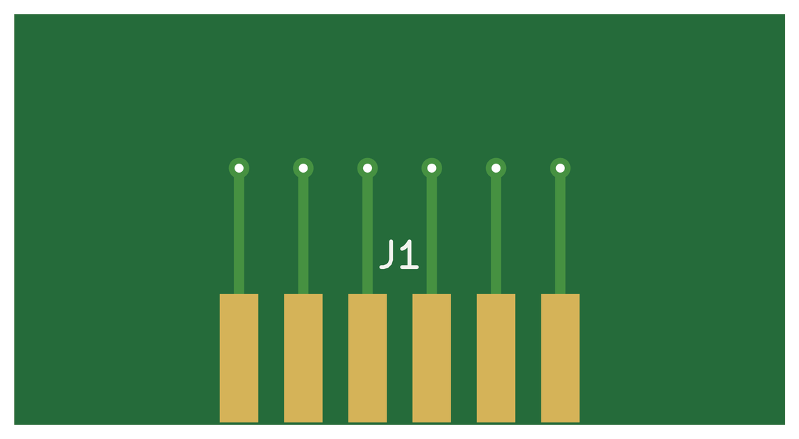
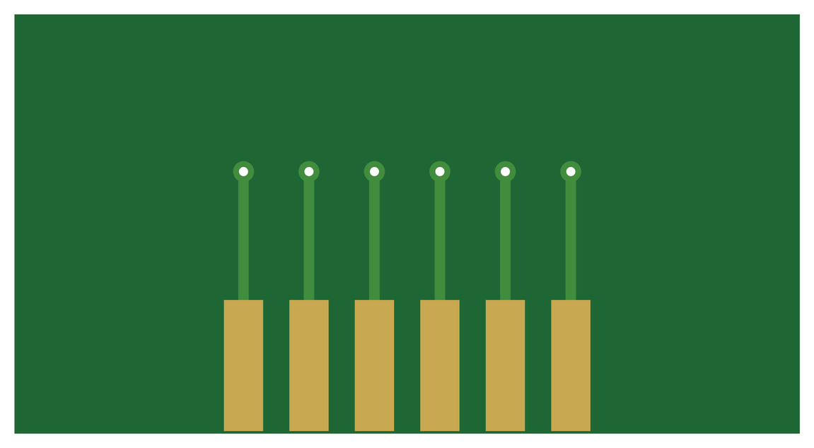
| Mode and format | 1–2 read | 3 resolve | 4 geometry | 5 materials | 6 assemble | 7 write | 8 verify | start-up and exit | Total |
|---|---|---|---|---|---|---|---|---|---|
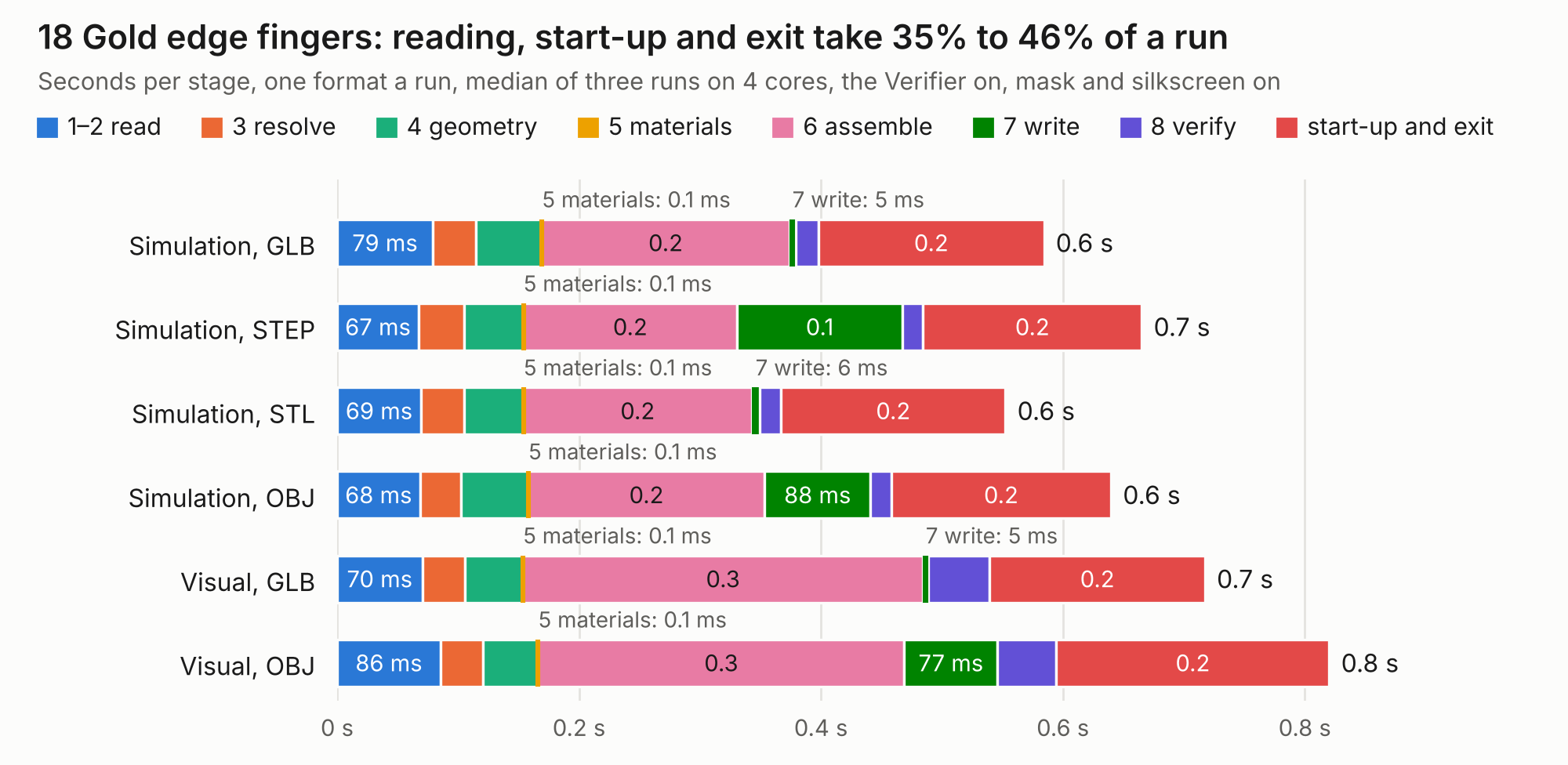
| Simulation, GLB | 79 ms | 35 ms | 55 ms | 0.1 ms | 0.2 | 5 ms | 19 ms | 0.2 | 0.6 |
| Simulation, STEP | 67 ms | 38 ms | 49 ms | 0.1 ms | 0.2 | 0.1 | 17 ms | 0.2 | 0.7 |
| Simulation, STL | 69 ms | 36 ms | 49 ms | 0.1 ms | 0.2 | 6 ms | 18 ms | 0.2 | 0.6 |
| Simulation, OBJ | 68 ms | 34 ms | 55 ms | 0.1 ms | 0.2 | 88 ms | 17 ms | 0.2 | 0.6 |
| Visual, GLB | 70 ms | 35 ms | 48 ms | 0.1 ms | 0.3 | 5 ms | 51 ms | 0.2 | 0.7 |
| Visual, OBJ | 86 ms | 35 ms | 46 ms | 0.1 ms | 0.3 | 77 ms | 49 ms | 0.2 | 0.8 |
|
|
|||||||||||||||||||||||||||||||||||||||||
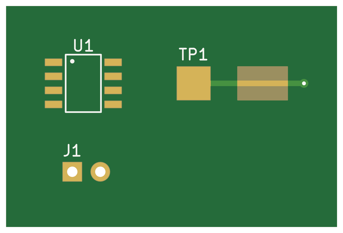
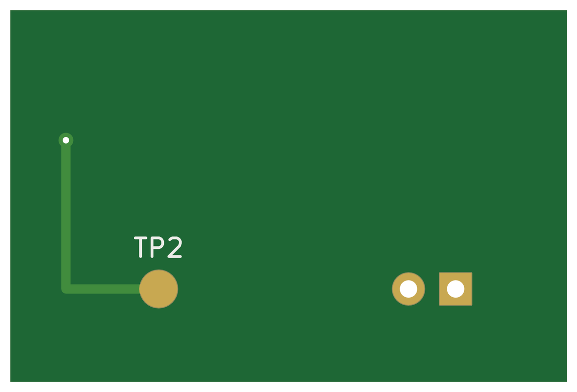
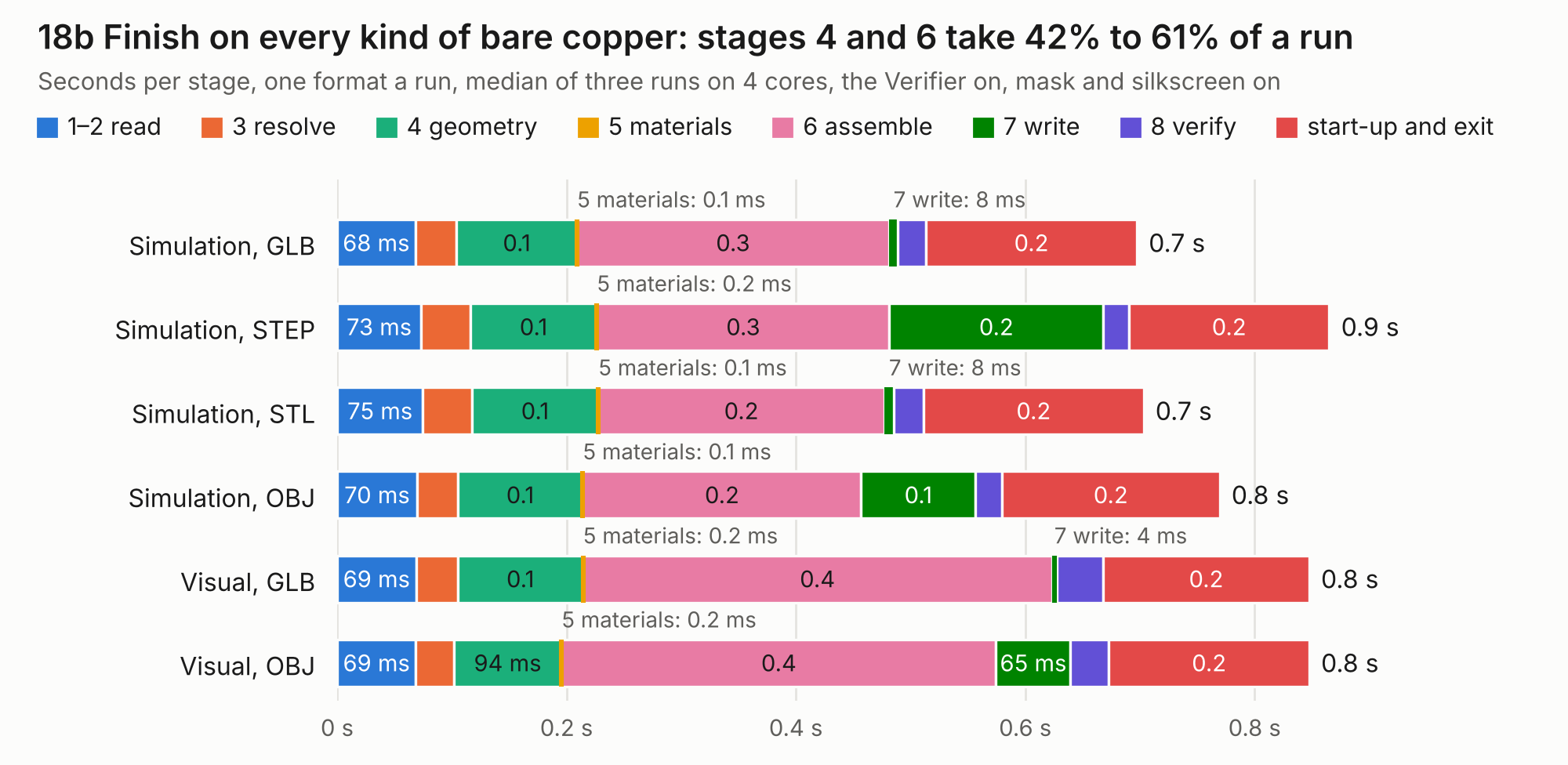
| Mode and format | 1–2 read | 3 resolve | 4 geometry | 5 materials | 6 assemble | 7 write | 8 verify | start-up and exit | Total |
|---|---|---|---|---|---|---|---|---|---|
| Simulation, GLB | 68 ms | 36 ms | 0.1 | 0.1 ms | 0.3 | 8 ms | 24 ms | 0.2 | 0.7 |
| Simulation, STEP | 73 ms | 43 ms | 0.1 | 0.2 ms | 0.3 | 0.2 | 22 ms | 0.2 | 0.9 |
| Simulation, STL | 75 ms | 43 ms | 0.1 | 0.1 ms | 0.2 | 8 ms | 26 ms | 0.2 | 0.7 |
| Simulation, OBJ | 70 ms | 35 ms | 0.1 | 0.1 ms | 0.2 | 0.1 | 23 ms | 0.2 | 0.8 |
| Visual, GLB | 69 ms | 36 ms | 0.1 | 0.2 ms | 0.4 | 4 ms | 40 ms | 0.2 | 0.8 |
| Visual, OBJ | 69 ms | 33 ms | 94 ms | 0.2 ms | 0.4 | 65 ms | 33 ms | 0.2 | 0.8 |
|
|
|||||||||||||||||||||||||||||||||||||||||
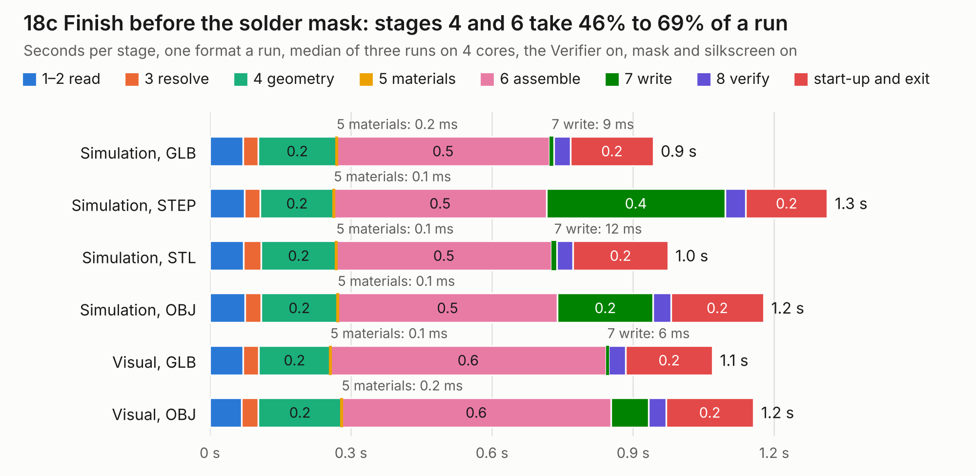
| Mode and format | 1–2 read | 3 resolve | 4 geometry | 5 materials | 6 assemble | 7 write | 8 verify | start-up and exit | Total |
|---|---|---|---|---|---|---|---|---|---|
| Simulation, GLB | 70 ms | 32 ms | 0.2 | 0.2 ms | 0.5 | 9 ms | 36 ms | 0.2 | 0.9 |
| Simulation, STEP | 74 ms | 33 ms | 0.2 | 0.1 ms | 0.5 | 0.4 | 43 ms | 0.2 | 1.3 |
| Simulation, STL | 71 ms | 37 ms | 0.2 | 0.1 ms | 0.5 | 12 ms | 34 ms | 0.2 | 1.0 |
| Simulation, OBJ | 74 ms | 35 ms | 0.2 | 0.1 ms | 0.5 | 0.2 | 38 ms | 0.2 | 1.2 |
| Visual, GLB | 70 ms | 34 ms | 0.2 | 0.1 ms | 0.6 | 6 ms | 36 ms | 0.2 | 1.1 |
| Visual, OBJ | 68 ms | 35 ms | 0.2 | 0.2 ms | 0.6 | 80 ms | 37 ms | 0.2 | 1.2 |
|
|
|||||||||||||||||||||||||||||||||||||||||
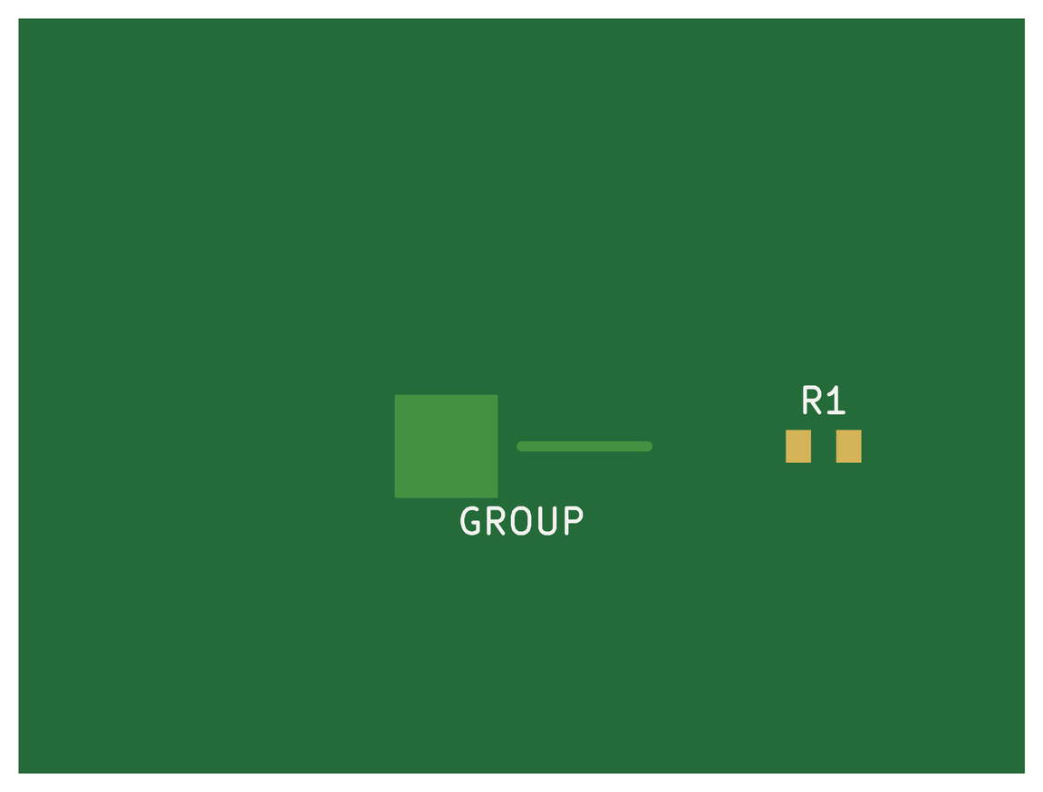

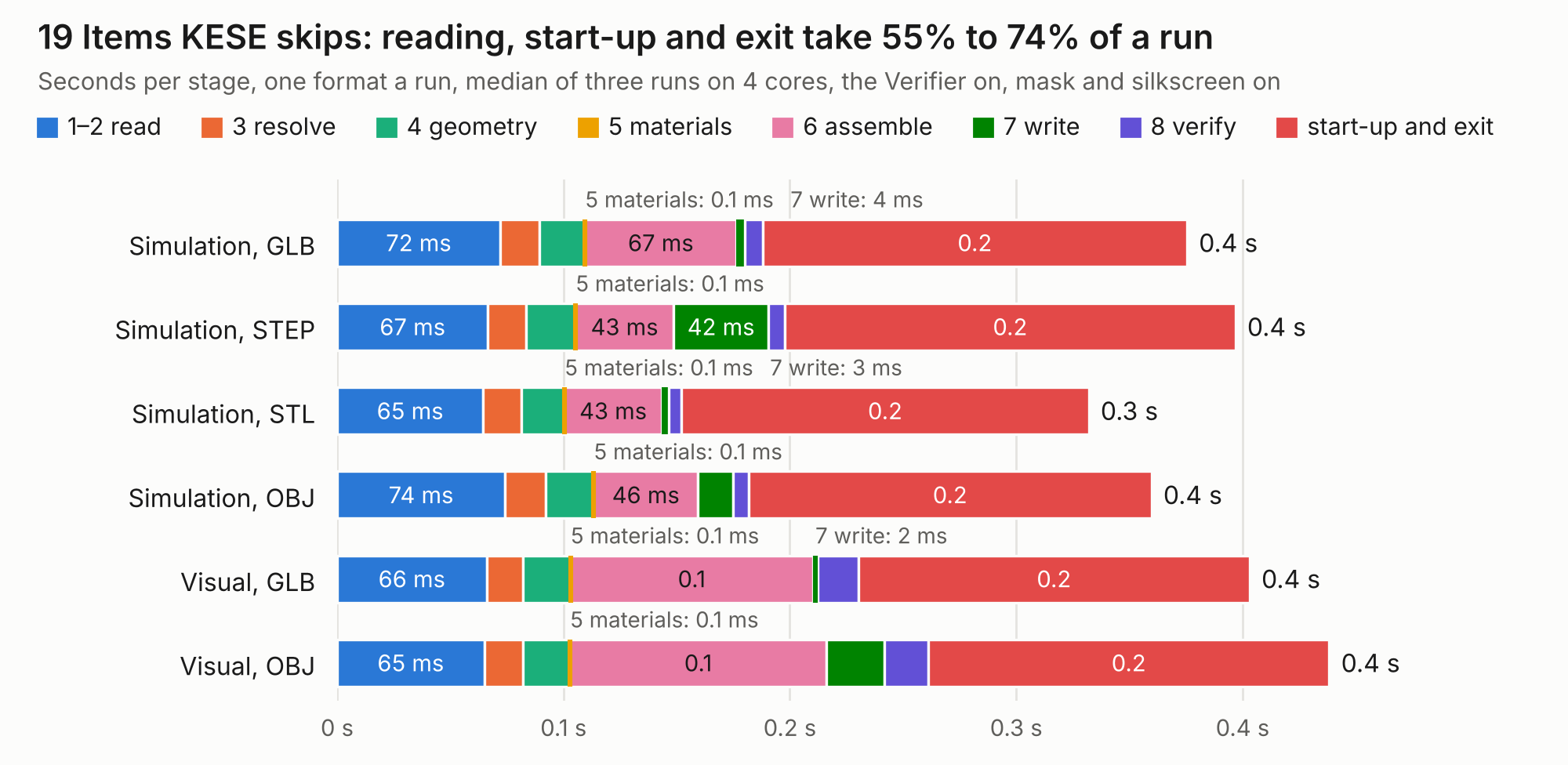
| Mode and format | 1–2 read | 3 resolve | 4 geometry | 5 materials | 6 assemble | 7 write | 8 verify | start-up and exit | Total |
|---|---|---|---|---|---|---|---|---|---|
| Simulation, GLB | 72 ms | 17 ms | 20 ms | 0.1 ms | 67 ms | 4 ms | 8 ms | 0.2 | 0.4 |
| Simulation, STEP | 67 ms | 17 ms | 22 ms | 0.1 ms | 43 ms | 42 ms | 7 ms | 0.2 | 0.4 |
| Simulation, STL | 65 ms | 17 ms | 19 ms | 0.1 ms | 43 ms | 3 ms | 6 ms | 0.2 | 0.3 |
| Simulation, OBJ | 74 ms | 18 ms | 21 ms | 0.1 ms | 46 ms | 16 ms | 7 ms | 0.2 | 0.4 |
| Visual, GLB | 66 ms | 16 ms | 21 ms | 0.1 ms | 0.1 | 2 ms | 18 ms | 0.2 | 0.4 |
| Visual, OBJ | 65 ms | 17 ms | 21 ms | 0.1 ms | 0.1 | 26 ms | 19 ms | 0.2 | 0.4 |
|
|
|||||||||||||||||||||||||||||||||||||||||


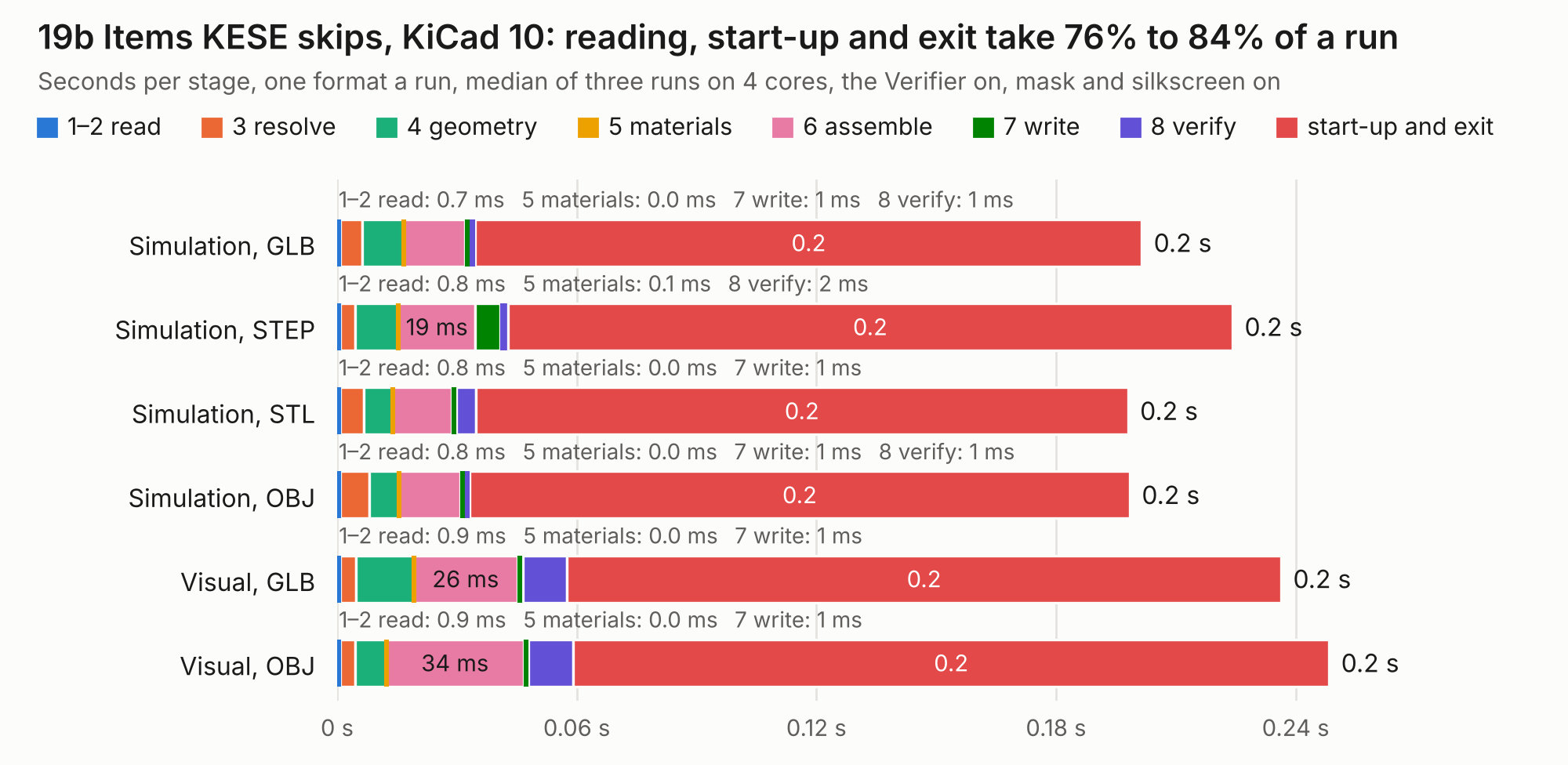
| Mode and format | 1–2 read | 3 resolve | 4 geometry | 5 materials | 6 assemble | 7 write | 8 verify | start-up and exit | Total |
|---|---|---|---|---|---|---|---|---|---|
| Simulation, GLB | 0.7 ms | 6 ms | 10 ms | 0.0 ms | 15 ms | 1 ms | 1 ms | 0.2 | 0.2 |
| Simulation, STEP | 0.8 ms | 4 ms | 11 ms | 0.1 ms | 19 ms | 6 ms | 2 ms | 0.2 | 0.2 |
| Simulation, STL | 0.8 ms | 6 ms | 7 ms | 0.0 ms | 15 ms | 1 ms | 5 ms | 0.2 | 0.2 |
| Simulation, OBJ | 0.8 ms | 7 ms | 8 ms | 0.0 ms | 15 ms | 1 ms | 1 ms | 0.2 | 0.2 |
| Visual, GLB | 0.9 ms | 4 ms | 15 ms | 0.0 ms | 26 ms | 1 ms | 11 ms | 0.2 | 0.2 |
| Visual, OBJ | 0.9 ms | 4 ms | 8 ms | 0.0 ms | 34 ms | 1 ms | 11 ms | 0.2 | 0.2 |
|
|
|||||||||||||||||||||||||||||||||||||||||
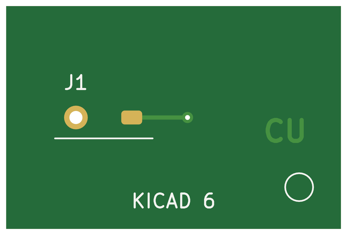
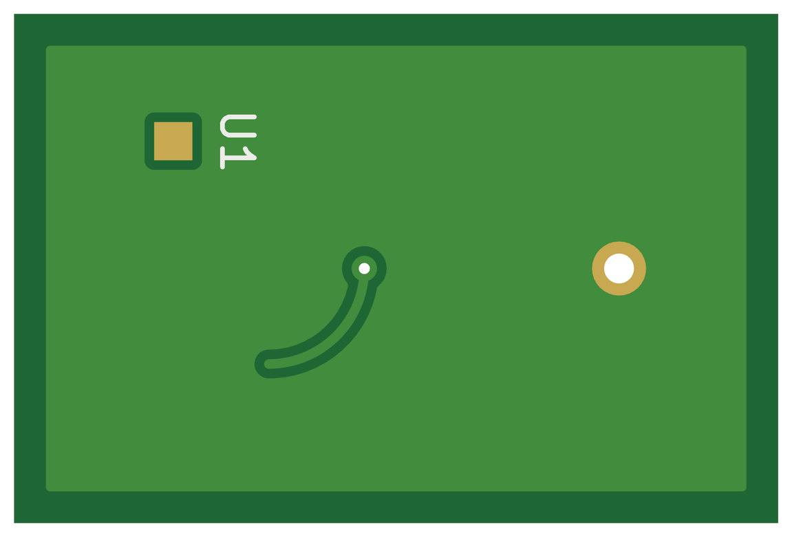
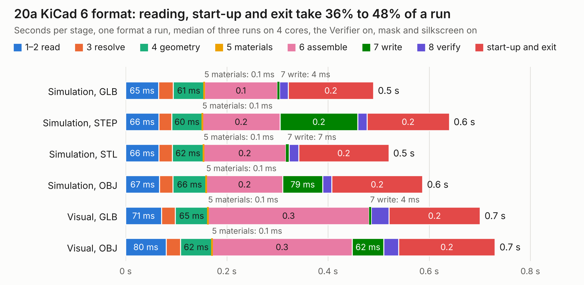
| Mode and format | 1–2 read | 3 resolve | 4 geometry | 5 materials | 6 assemble | 7 write | 8 verify | start-up and exit | Total |
|---|---|---|---|---|---|---|---|---|---|
| Simulation, GLB | 65 ms | 29 ms | 61 ms | 0.1 ms | 0.1 | 4 ms | 17 ms | 0.2 | 0.5 |
| Simulation, STEP | 66 ms | 25 ms | 60 ms | 0.1 ms | 0.2 | 0.2 | 18 ms | 0.2 | 0.6 |
| Simulation, STL | 66 ms | 27 ms | 62 ms | 0.1 ms | 0.2 | 7 ms | 19 ms | 0.2 | 0.5 |
| Simulation, OBJ | 67 ms | 26 ms | 66 ms | 0.1 ms | 0.2 | 79 ms | 18 ms | 0.2 | 0.6 |
| Visual, GLB | 71 ms | 27 ms | 65 ms | 0.1 ms | 0.3 | 4 ms | 35 ms | 0.2 | 0.7 |
| Visual, OBJ | 80 ms | 29 ms | 62 ms | 0.1 ms | 0.3 | 62 ms | 29 ms | 0.2 | 0.7 |
|
|
|||||||||||||||||||||||||||||||||||||||||
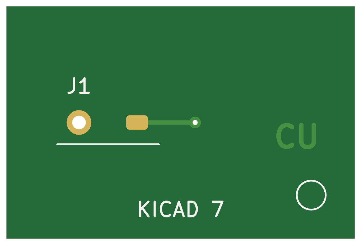
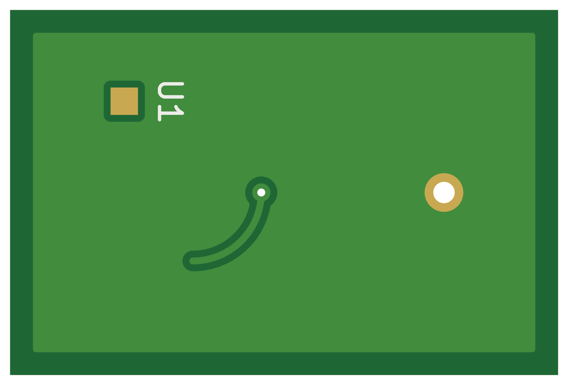
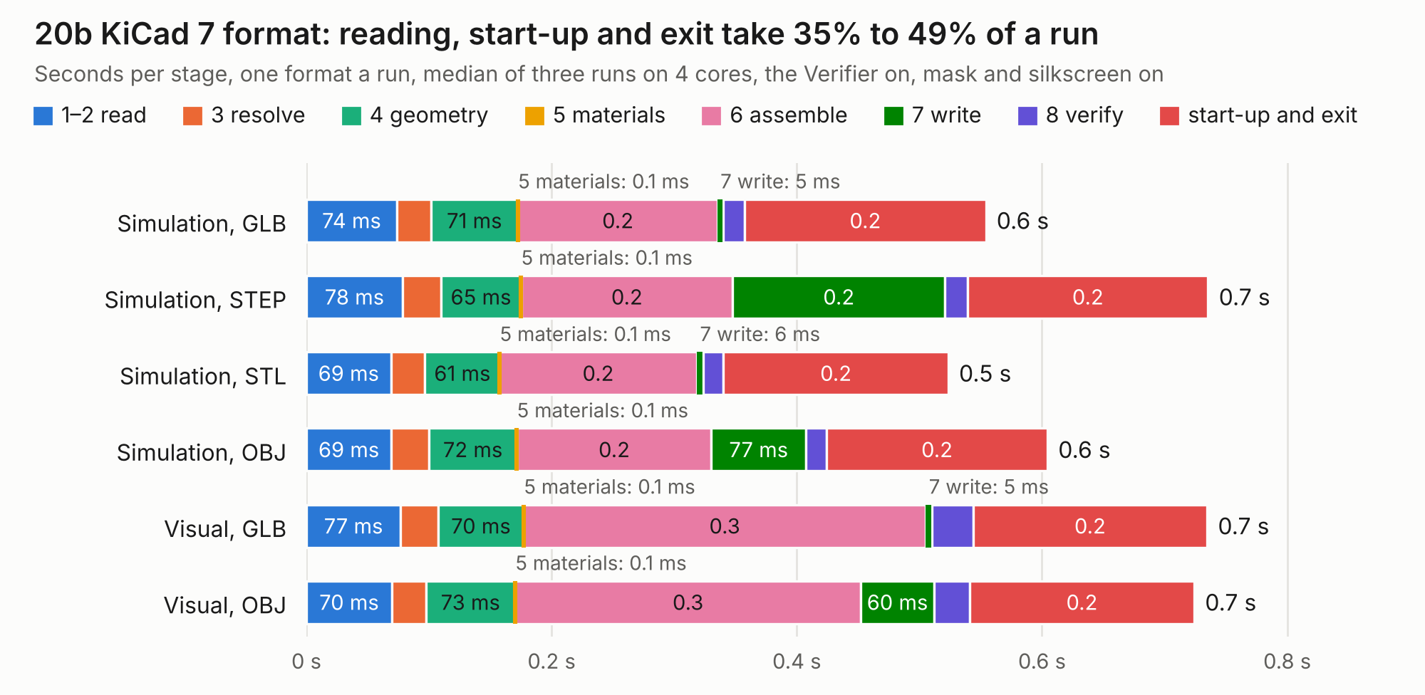
| Mode and format | 1–2 read | 3 resolve | 4 geometry | 5 materials | 6 assemble | 7 write | 8 verify | start-up and exit | Total |
|---|---|---|---|---|---|---|---|---|---|
| Simulation, GLB | 74 ms | 28 ms | 71 ms | 0.1 ms | 0.2 | 5 ms | 18 ms | 0.2 | 0.6 |
| Simulation, STEP | 78 ms | 31 ms | 65 ms | 0.1 ms | 0.2 | 0.2 | 19 ms | 0.2 | 0.7 |
| Simulation, STL | 69 ms | 28 ms | 61 ms | 0.1 ms | 0.2 | 6 ms | 16 ms | 0.2 | 0.5 |
| Simulation, OBJ | 69 ms | 31 ms | 72 ms | 0.1 ms | 0.2 | 77 ms | 17 ms | 0.2 | 0.6 |
| Visual, GLB | 77 ms | 31 ms | 70 ms | 0.1 ms | 0.3 | 5 ms | 33 ms | 0.2 | 0.7 |
| Visual, OBJ | 70 ms | 28 ms | 73 ms | 0.1 ms | 0.3 | 60 ms | 29 ms | 0.2 | 0.7 |
|
|
|||||||||||||||||||||||||||||||||||||||||
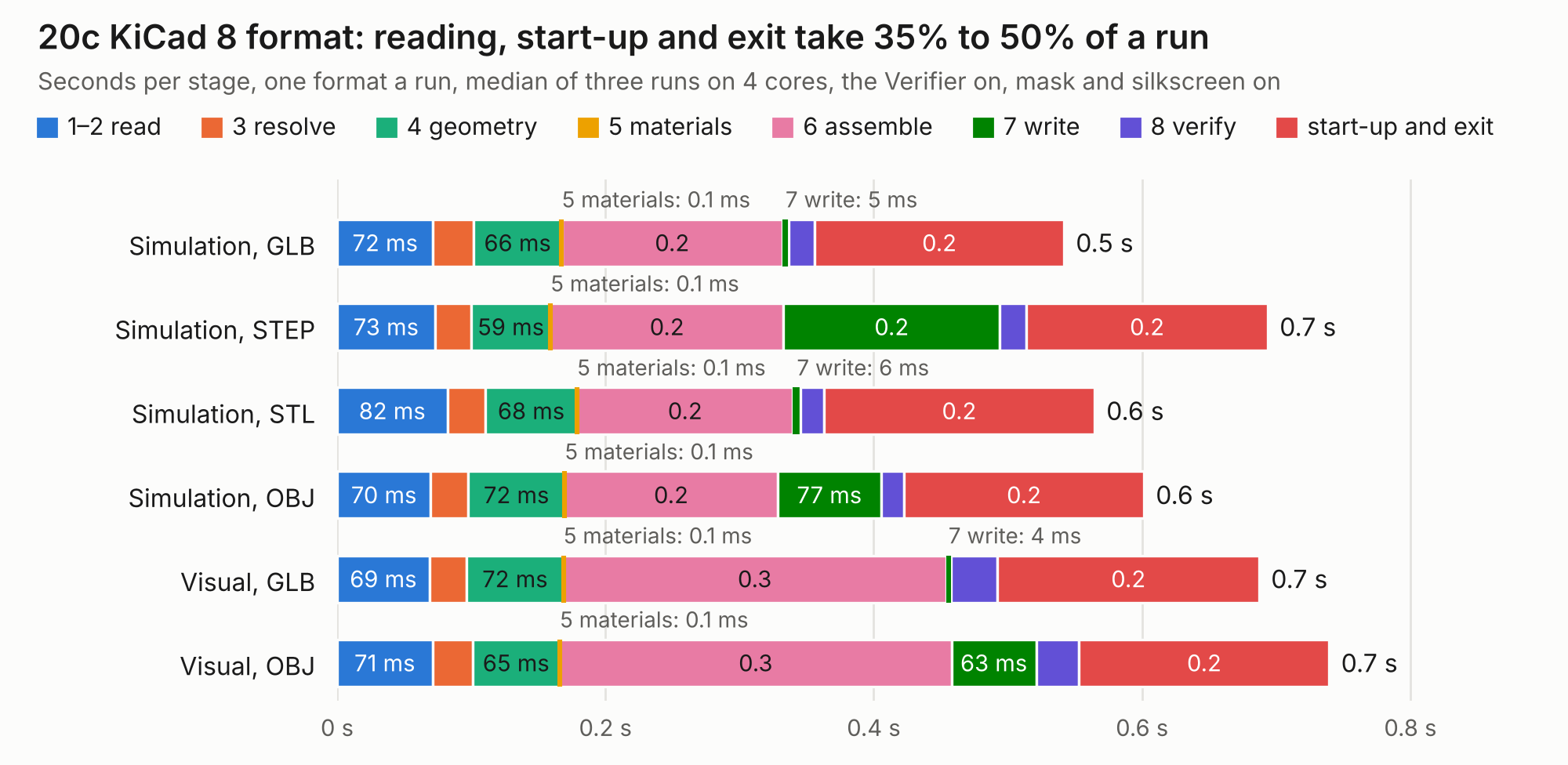
| Mode and format | 1–2 read | 3 resolve | 4 geometry | 5 materials | 6 assemble | 7 write | 8 verify | start-up and exit | Total |
|---|---|---|---|---|---|---|---|---|---|
| Simulation, GLB | 72 ms | 30 ms | 66 ms | 0.1 ms | 0.2 | 5 ms | 19 ms | 0.2 | 0.5 |
| Simulation, STEP | 73 ms | 27 ms | 59 ms | 0.1 ms | 0.2 | 0.2 | 20 ms | 0.2 | 0.7 |
| Simulation, STL | 82 ms | 28 ms | 68 ms | 0.1 ms | 0.2 | 6 ms | 17 ms | 0.2 | 0.6 |
| Simulation, OBJ | 70 ms | 28 ms | 72 ms | 0.1 ms | 0.2 | 77 ms | 17 ms | 0.2 | 0.6 |
| Visual, GLB | 69 ms | 28 ms | 72 ms | 0.1 ms | 0.3 | 4 ms | 35 ms | 0.2 | 0.7 |
| Visual, OBJ | 71 ms | 30 ms | 65 ms | 0.1 ms | 0.3 | 63 ms | 32 ms | 0.2 | 0.7 |
|
|
|||||||||||||||||||||||||||||||||||||||||
| Mode and format | 1–2 read | 3 resolve | 4 geometry | 5 materials | 6 assemble | 7 write | 8 verify | start-up and exit | Total |
|---|---|---|---|---|---|---|---|---|---|
| Simulation, GLB | 75 ms | 29 ms | 68 ms | 0.1 ms | 0.2 | 5 ms | 17 ms | 0.2 | 0.6 |
| Simulation, STEP | 67 ms | 33 ms | 66 ms | 0.1 ms | 0.2 | 0.2 | 17 ms | 0.2 | 0.7 |
| Simulation, STL | 69 ms | 34 ms | 64 ms | 0.1 ms | 0.2 | 7 ms | 16 ms | 0.2 | 0.5 |
| Simulation, OBJ | 70 ms | 29 ms | 67 ms | 0.1 ms | 0.2 | 74 ms | 19 ms | 0.2 | 0.6 |
| Visual, GLB | 68 ms | 28 ms | 71 ms | 0.1 ms | 0.3 | 4 ms | 30 ms | 0.2 | 0.7 |
| Visual, OBJ | 67 ms | 27 ms | 69 ms | 0.1 ms | 0.3 | 59 ms | 31 ms | 0.2 | 0.7 |
|
|
|||||||||||||||||||||||||||||||||||||||||
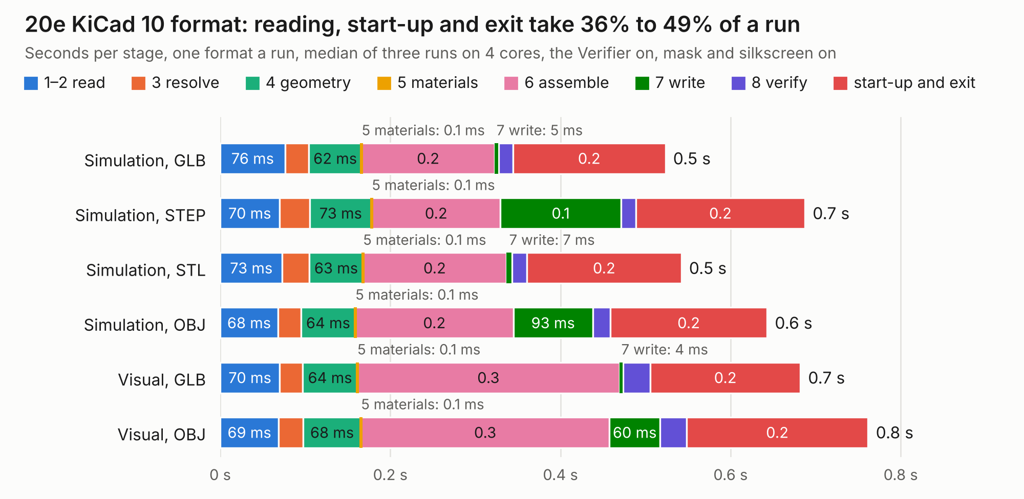
| Mode and format | 1–2 read | 3 resolve | 4 geometry | 5 materials | 6 assemble | 7 write | 8 verify | start-up and exit | Total |
|---|---|---|---|---|---|---|---|---|---|
| Simulation, GLB | 76 ms | 28 ms | 62 ms | 0.1 ms | 0.2 | 5 ms | 17 ms | 0.2 | 0.5 |
| Simulation, STEP | 70 ms | 36 ms | 73 ms | 0.1 ms | 0.2 | 0.1 | 17 ms | 0.2 | 0.7 |
| Simulation, STL | 73 ms | 32 ms | 63 ms | 0.1 ms | 0.2 | 7 ms | 17 ms | 0.2 | 0.5 |
| Simulation, OBJ | 68 ms | 27 ms | 64 ms | 0.1 ms | 0.2 | 93 ms | 21 ms | 0.2 | 0.6 |
| Visual, GLB | 70 ms | 27 ms | 64 ms | 0.1 ms | 0.3 | 4 ms | 32 ms | 0.2 | 0.7 |
| Visual, OBJ | 69 ms | 29 ms | 68 ms | 0.1 ms | 0.3 | 60 ms | 31 ms | 0.2 | 0.8 |
|
|
|||||||||||||||||||||||||||||||||||||||||
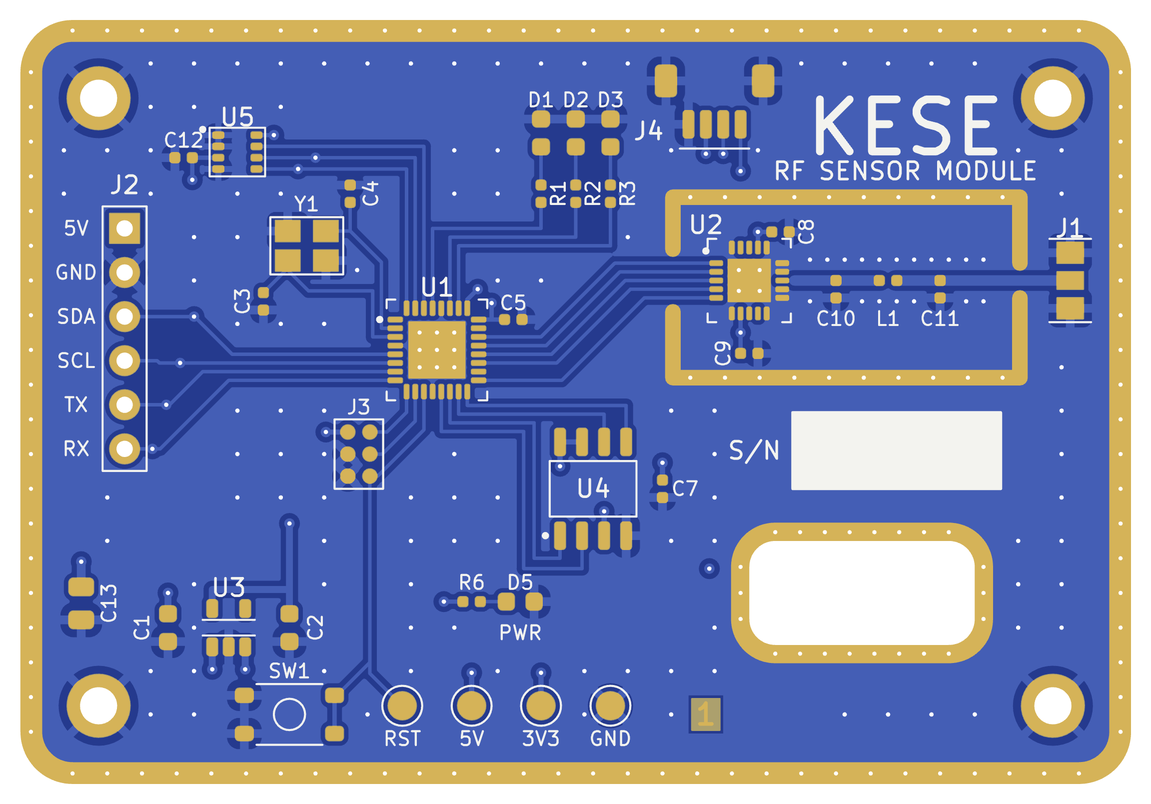
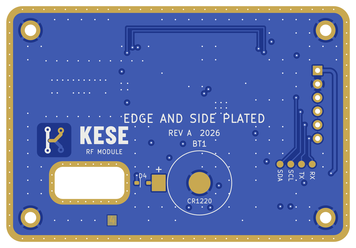
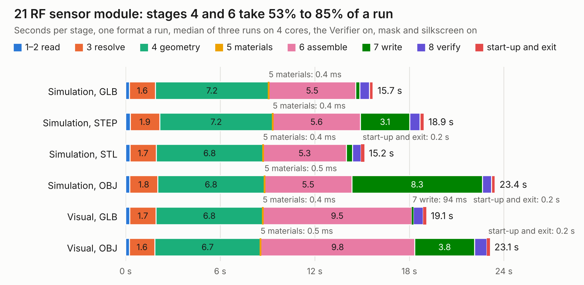
| Mode and format | 1–2 read | 3 resolve | 4 geometry | 5 materials | 6 assemble | 7 write | 8 verify | start-up and exit | Total |
|---|---|---|---|---|---|---|---|---|---|
| Simulation, GLB | 0.2 | 1.6 | 7.2 | 0.4 ms | 5.5 | 0.3 | 0.6 | 0.2 | 15.7 |
| Simulation, STEP | 0.3 | 1.9 | 7.2 | 0.4 ms | 5.6 | 3.1 | 0.6 | 0.3 | 18.9 |
| Simulation, STL | 0.3 | 1.7 | 6.8 | 0.4 ms | 5.3 | 0.4 | 0.5 | 0.2 | 15.2 |
| Simulation, OBJ | 0.3 | 1.8 | 6.8 | 0.5 ms | 5.5 | 8.3 | 0.6 | 0.2 | 23.4 |
| Visual, GLB | 0.3 | 1.7 | 6.8 | 0.4 ms | 9.5 | 94 ms | 0.6 | 0.2 | 19.1 |
| Visual, OBJ | 0.2 | 1.6 | 6.7 | 0.5 ms | 9.8 | 3.8 | 0.8 | 0.2 | 23.1 |
|
|
|||||||||||||||||||||||||||||||||||||||||
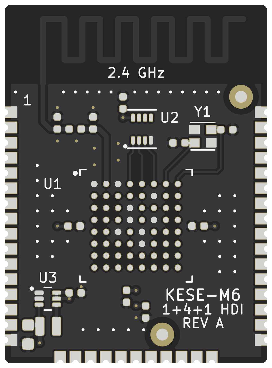
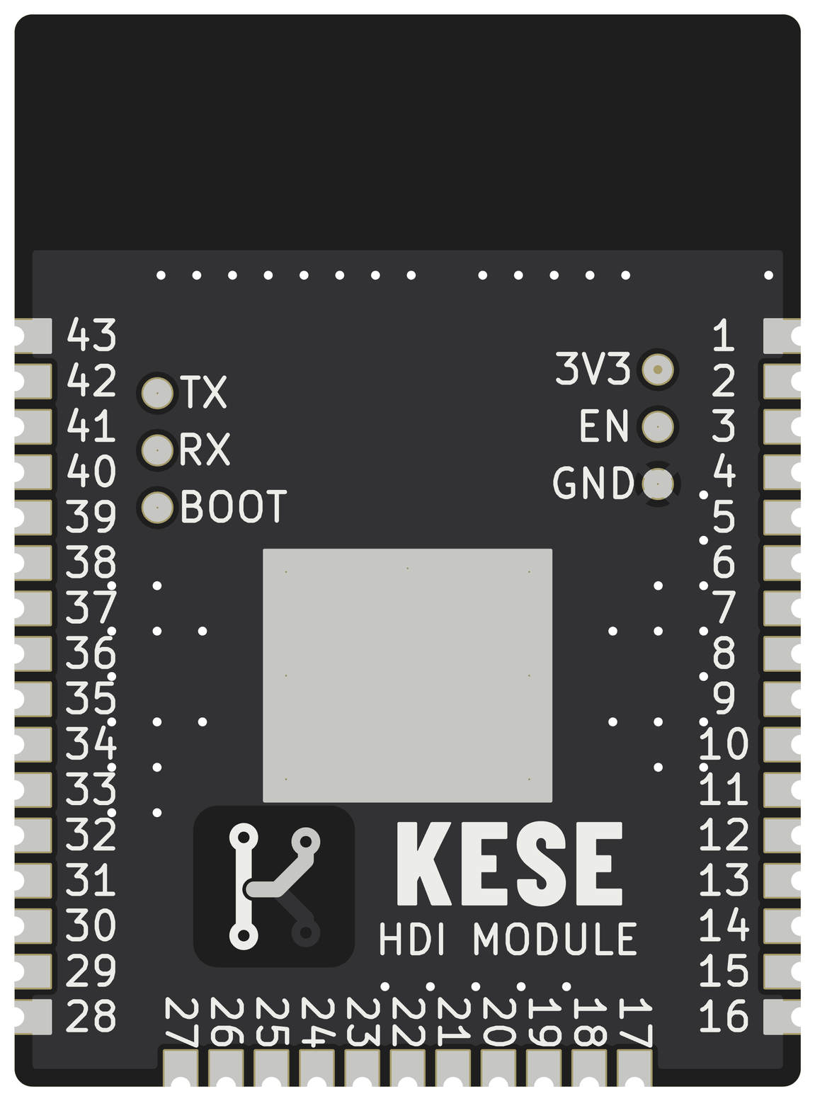
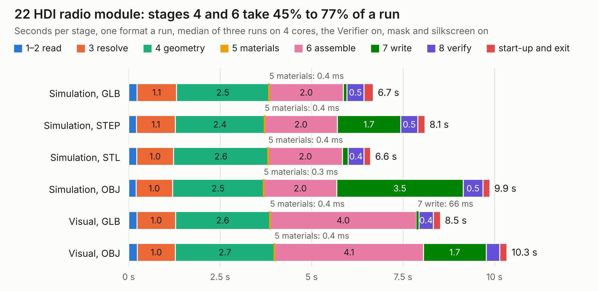
| Mode and format | 1–2 read | 3 resolve | 4 geometry | 5 materials | 6 assemble | 7 write | 8 verify | start-up and exit | Total |
|---|---|---|---|---|---|---|---|---|---|
| Simulation, GLB | 0.2 | 1.1 | 2.5 | 0.4 ms | 2.0 | 0.1 | 0.5 | 0.3 | 6.7 |
| Simulation, STEP | 0.2 | 1.1 | 2.4 | 0.4 ms | 2.0 | 1.7 | 0.5 | 0.2 | 8.1 |
| Simulation, STL | 0.2 | 1.0 | 2.6 | 0.4 ms | 2.0 | 0.2 | 0.4 | 0.2 | 6.6 |
| Simulation, OBJ | 0.2 | 1.0 | 2.5 | 0.3 ms | 2.0 | 3.5 | 0.5 | 0.2 | 9.9 |
| Visual, GLB | 0.2 | 1.0 | 2.6 | 0.4 ms | 4.0 | 66 ms | 0.4 | 0.2 | 8.5 |
| Visual, OBJ | 0.2 | 1.0 | 2.7 | 0.4 ms | 4.1 | 1.7 | 0.4 | 0.2 | 10.3 |
|
|
|||||||||||||||||||||||||||||||||||||||||
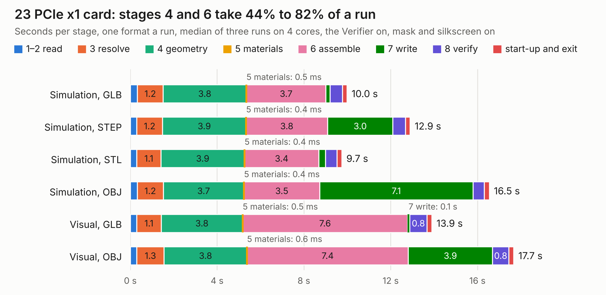
| Mode and format | 1–2 read | 3 resolve | 4 geometry | 5 materials | 6 assemble | 7 write | 8 verify | start-up and exit | Total |
|---|---|---|---|---|---|---|---|---|---|
| Simulation, GLB | 0.3 | 1.2 | 3.8 | 0.5 ms | 3.7 | 0.2 | 0.6 | 0.2 | 10.0 |
| Simulation, STEP | 0.3 | 1.2 | 3.9 | 0.4 ms | 3.8 | 3.0 | 0.6 | 0.2 | 12.9 |
| Simulation, STL | 0.3 | 1.1 | 3.9 | 0.4 ms | 3.4 | 0.3 | 0.5 | 0.2 | 9.7 |
| Simulation, OBJ | 0.3 | 1.2 | 3.7 | 0.4 ms | 3.5 | 7.1 | 0.5 | 0.2 | 16.5 |
| Visual, GLB | 0.3 | 1.1 | 3.8 | 0.5 ms | 7.6 | 0.1 | 0.8 | 0.2 | 13.9 |
| Visual, OBJ | 0.3 | 1.3 | 3.8 | 0.6 ms | 7.4 | 3.9 | 0.8 | 0.2 | 17.7 |
|
|
|||||||||||||||||||||||||||||||||||||||||
Seconds, the median of three runs for each stage, unless marked ms; the total is the sum of the bars.
| Board | Mode and format | 1–2 read | 3 resolve | 4 geometry | 5 materials | 6 assemble | 7 write | 8 verify | start-up and exit | Total |
|---|---|---|---|---|---|---|---|---|---|---|
| 01 Slotted holes | simulation, GLB | 70 ms | 56 ms | 0.2 | 0.2 ms | 0.3 | 8 ms | 41 ms | 0.2 | 0.9 |
| 01 Slotted holes | simulation, STEP | 74 ms | 55 ms | 0.2 | 0.1 ms | 0.4 | 0.4 | 36 ms | 0.2 | 1.3 |
| 01 Slotted holes | simulation, STL | 69 ms | 51 ms | 0.2 | 0.1 ms | 0.4 | 11 ms | 40 ms | 0.2 | 0.9 |
| 01 Slotted holes | simulation, OBJ | 74 ms | 53 ms | 0.2 | 0.1 ms | 0.4 | 0.2 | 41 ms | 0.2 | 1.2 |
| 01 Slotted holes | visual, GLB | 83 ms | 56 ms | 0.2 | 0.1 ms | 0.5 | 7 ms | 40 ms | 0.2 | 1.1 |
| 01 Slotted holes | visual, OBJ | 68 ms | 53 ms | 0.2 | 0.2 ms | 0.5 | 0.1 | 40 ms | 0.2 | 1.2 |
| 02 Round holes | simulation, GLB | 76 ms | 45 ms | 0.2 | 0.1 ms | 0.4 | 8 ms | 34 ms | 0.2 | 0.9 |
| 02 Round holes | simulation, STEP | 73 ms | 46 ms | 0.2 | 0.1 ms | 0.4 | 0.3 | 31 ms | 0.2 | 1.2 |
| 02 Round holes | simulation, STL | 67 ms | 42 ms | 0.2 | 0.1 ms | 0.4 | 12 ms | 31 ms | 0.2 | 0.9 |
| 02 Round holes | simulation, OBJ | 72 ms | 49 ms | 0.2 | 0.1 ms | 0.4 | 0.2 | 31 ms | 0.2 | 1.1 |
| 02 Round holes | visual, GLB | 71 ms | 46 ms | 0.2 | 0.1 ms | 0.4 | 6 ms | 42 ms | 0.2 | 1.0 |
| 02 Round holes | visual, OBJ | 66 ms | 39 ms | 0.2 | 0.1 ms | 0.4 | 0.1 | 43 ms | 0.2 | 1.1 |
| 03 Through vias | simulation, GLB | 67 ms | 51 ms | 0.2 | 0.1 ms | 0.5 | 11 ms | 44 ms | 0.2 | 1.2 |
| 03 Through vias | simulation, STEP | 71 ms | 58 ms | 0.2 | 0.1 ms | 0.6 | 0.3 | 49 ms | 0.2 | 1.6 |
| 03 Through vias | simulation, STL | 67 ms | 51 ms | 0.2 | 0.1 ms | 0.6 | 20 ms | 48 ms | 0.2 | 1.2 |
| 03 Through vias | simulation, OBJ | 66 ms | 55 ms | 0.2 | 0.1 ms | 0.6 | 0.3 | 55 ms | 0.2 | 1.5 |
| 03 Through vias | visual, GLB | 67 ms | 55 ms | 0.2 | 0.1 ms | 0.6 | 6 ms | 67 ms | 0.2 | 1.2 |
| 03 Through vias | visual, OBJ | 82 ms | 60 ms | 0.2 | 0.1 ms | 0.6 | 0.1 | 60 ms | 0.2 | 1.3 |
| 03b KiCad 10 via options | simulation, GLB | 69 ms | 0.1 | 0.3 | 0.1 ms | 0.7 | 16 ms | 0.1 | 0.2 | 1.5 |
| 03b KiCad 10 via options | simulation, STEP | 80 ms | 0.2 | 0.3 | 0.1 ms | 0.6 | 0.7 | 0.1 | 0.2 | 2.2 |
| 03b KiCad 10 via options | simulation, STL | 76 ms | 0.1 | 0.3 | 0.2 ms | 0.6 | 25 ms | 97 ms | 0.2 | 1.4 |
| 03b KiCad 10 via options | simulation, OBJ | 75 ms | 0.1 | 0.3 | 0.2 ms | 0.6 | 0.4 | 94 ms | 0.2 | 1.8 |
| 03b KiCad 10 via options | visual, GLB | 92 ms | 0.2 | 0.3 | 0.1 ms | 2.4 | 14 ms | 90 ms | 0.2 | 3.2 |
| 03b KiCad 10 via options | visual, OBJ | 74 ms | 0.2 | 0.3 | 0.1 ms | 2.4 | 0.3 | 78 ms | 0.2 | 3.5 |
| 04 Blind and buried vias | simulation, GLB | 73 ms | 51 ms | 62 ms | 0.1 ms | 0.2 | 5 ms | 26 ms | 0.2 | 0.7 |
| 04 Blind and buried vias | simulation, STEP | 68 ms | 50 ms | 59 ms | 0.1 ms | 0.2 | 0.2 | 22 ms | 0.2 | 0.8 |
| 04 Blind and buried vias | simulation, STL | 68 ms | 51 ms | 59 ms | 0.1 ms | 0.2 | 8 ms | 21 ms | 0.2 | 0.6 |
| 04 Blind and buried vias | simulation, OBJ | 66 ms | 55 ms | 62 ms | 0.1 ms | 0.2 | 0.1 | 22 ms | 0.2 | 0.7 |
| 04 Blind and buried vias | visual, GLB | 70 ms | 54 ms | 59 ms | 0.1 ms | 0.4 | 5 ms | 37 ms | 0.2 | 0.8 |
| 04 Blind and buried vias | visual, OBJ | 69 ms | 53 ms | 63 ms | 0.1 ms | 0.4 | 47 ms | 32 ms | 0.2 | 0.8 |
| 05 Microvias | simulation, GLB | 3 ms | 54 ms | 61 ms | 0.1 ms | 0.2 | 5 ms | 21 ms | 0.2 | 0.6 |
| 05 Microvias | simulation, STEP | 3 ms | 55 ms | 49 ms | 0.1 ms | 0.2 | 0.1 | 20 ms | 0.2 | 0.6 |
| 05 Microvias | simulation, STL | 3 ms | 50 ms | 57 ms | 0.1 ms | 0.2 | 6 ms | 25 ms | 0.2 | 0.6 |
| 05 Microvias | simulation, OBJ | 3 ms | 58 ms | 49 ms | 0.1 ms | 0.2 | 97 ms | 22 ms | 0.2 | 0.6 |
| 05 Microvias | visual, GLB | 4 ms | 60 ms | 52 ms | 0.1 ms | 0.3 | 3 ms | 49 ms | 0.2 | 0.7 |
| 05 Microvias | visual, OBJ | 3 ms | 59 ms | 55 ms | 0.1 ms | 0.3 | 30 ms | 49 ms | 0.2 | 0.7 |
| 06 Padstacks | simulation, GLB | 68 ms | 48 ms | 92 ms | 0.1 ms | 0.3 | 7 ms | 29 ms | 0.2 | 0.7 |
| 06 Padstacks | simulation, STEP | 69 ms | 47 ms | 99 ms | 0.1 ms | 0.3 | 0.2 | 30 ms | 0.2 | 1.0 |
| 06 Padstacks | simulation, STL | 71 ms | 51 ms | 93 ms | 0.1 ms | 0.3 | 9 ms | 32 ms | 0.2 | 0.8 |
| 06 Padstacks | simulation, OBJ | 80 ms | 46 ms | 89 ms | 0.1 ms | 0.3 | 0.2 | 35 ms | 0.2 | 0.9 |
| 06 Padstacks | visual, GLB | 65 ms | 47 ms | 0.1 | 0.1 ms | 0.5 | 4 ms | 33 ms | 0.2 | 0.9 |
| 06 Padstacks | visual, OBJ | 68 ms | 48 ms | 93 ms | 0.1 ms | 0.4 | 73 ms | 32 ms | 0.2 | 0.9 |
| 07 Pad shapes | simulation, GLB | 74 ms | 40 ms | 0.1 | 0.1 ms | 0.3 | 9 ms | 25 ms | 0.2 | 0.7 |
| 07 Pad shapes | simulation, STEP | 77 ms | 44 ms | 0.1 | 0.1 ms | 0.3 | 0.3 | 25 ms | 0.2 | 1.0 |
| 07 Pad shapes | simulation, STL | 72 ms | 41 ms | 0.1 | 0.1 ms | 0.3 | 12 ms | 23 ms | 0.2 | 0.7 |
| 07 Pad shapes | simulation, OBJ | 90 ms | 37 ms | 0.1 | 0.1 ms | 0.3 | 0.1 | 22 ms | 0.2 | 0.9 |
| 07 Pad shapes | visual, GLB | 73 ms | 43 ms | 0.1 | 0.2 ms | 0.5 | 5 ms | 41 ms | 0.2 | 1.0 |
| 07 Pad shapes | visual, OBJ | 76 ms | 37 ms | 0.1 | 0.1 ms | 0.5 | 0.1 | 50 ms | 0.2 | 1.1 |
| 08 Copper graphics | simulation, GLB | 85 ms | 27 ms | 43 ms | 0.1 ms | 0.2 | 4 ms | 14 ms | 0.2 | 0.6 |
| 08 Copper graphics | simulation, STEP | 71 ms | 23 ms | 38 ms | 0.1 ms | 0.2 | 0.2 | 13 ms | 0.2 | 0.8 |
| 08 Copper graphics | simulation, STL | 73 ms | 24 ms | 38 ms | 0.1 ms | 0.2 | 6 ms | 13 ms | 0.2 | 0.6 |
| 08 Copper graphics | simulation, OBJ | 89 ms | 25 ms | 39 ms | 0.1 ms | 0.3 | 0.1 | 19 ms | 0.2 | 0.8 |
| 08 Copper graphics | visual, GLB | 70 ms | 23 ms | 39 ms | 0.1 ms | 0.3 | 4 ms | 40 ms | 0.2 | 0.7 |
| 08 Copper graphics | visual, OBJ | 69 ms | 25 ms | 41 ms | 0.1 ms | 0.3 | 96 ms | 51 ms | 0.2 | 0.7 |
| 08b Copper graphics on nets | simulation, GLB | 8 ms | 23 ms | 53 ms | 0.1 ms | 0.2 | 6 ms | 18 ms | 0.2 | 0.5 |
| 08b Copper graphics on nets | simulation, STEP | 7 ms | 31 ms | 54 ms | 0.1 ms | 0.2 | 0.2 | 17 ms | 0.2 | 0.7 |
| 08b Copper graphics on nets | simulation, STL | 7 ms | 28 ms | 55 ms | 0.2 ms | 0.3 | 11 ms | 21 ms | 0.2 | 0.6 |
| 08b Copper graphics on nets | simulation, OBJ | 7 ms | 29 ms | 60 ms | 0.1 ms | 0.2 | 94 ms | 19 ms | 0.2 | 0.6 |
| 08b Copper graphics on nets | visual, GLB | 11 ms | 32 ms | 59 ms | 0.1 ms | 0.4 | 4 ms | 42 ms | 0.2 | 0.7 |
| 08b Copper graphics on nets | visual, OBJ | 8 ms | 24 ms | 56 ms | 0.1 ms | 0.3 | 69 ms | 38 ms | 0.2 | 0.7 |
| 09 Copper text | simulation, GLB | 87 ms | 41 ms | 0.1 | 0.1 ms | 1.0 | 17 ms | 50 ms | 0.2 | 1.5 |
| 09 Copper text | simulation, STEP | 85 ms | 38 ms | 0.1 | 0.1 ms | 1.0 | 1.0 | 42 ms | 0.2 | 2.5 |
| 09 Copper text | simulation, STL | 87 ms | 38 ms | 0.1 | 0.1 ms | 1.1 | 34 ms | 47 ms | 0.2 | 1.6 |
| 09 Copper text | simulation, OBJ | 0.1 | 38 ms | 0.1 | 0.1 ms | 1.0 | 0.5 | 61 ms | 0.2 | 2.0 |
| 09 Copper text | visual, GLB | 88 ms | 38 ms | 0.1 | 0.1 ms | 0.9 | 12 ms | 86 ms | 0.2 | 1.4 |
| 09 Copper text | visual, OBJ | 87 ms | 40 ms | 0.1 | 0.1 ms | 0.9 | 0.4 | 98 ms | 0.2 | 1.9 |
| 10 Tracks and arcs | simulation, GLB | 71 ms | 24 ms | 37 ms | 0.1 ms | 0.2 | 7 ms | 19 ms | 0.2 | 0.6 |
| 10 Tracks and arcs | simulation, STEP | 74 ms | 27 ms | 36 ms | 0.1 ms | 0.2 | 0.2 | 16 ms | 0.2 | 0.8 |
| 10 Tracks and arcs | simulation, STL | 69 ms | 23 ms | 38 ms | 0.1 ms | 0.2 | 8 ms | 17 ms | 0.2 | 0.6 |
| 10 Tracks and arcs | simulation, OBJ | 68 ms | 24 ms | 46 ms | 0.1 ms | 0.2 | 83 ms | 16 ms | 0.2 | 0.6 |
| 10 Tracks and arcs | visual, GLB | 86 ms | 27 ms | 37 ms | 0.1 ms | 0.4 | 4 ms | 40 ms | 0.2 | 0.7 |
| 10 Tracks and arcs | visual, OBJ | 71 ms | 25 ms | 38 ms | 0.1 ms | 0.3 | 78 ms | 40 ms | 0.2 | 0.8 |
| 11 Zones | simulation, GLB | 0.1 | 0.1 | 0.4 | 0.1 ms | 0.6 | 19 ms | 80 ms | 0.2 | 1.5 |
| 11 Zones | simulation, STEP | 89 ms | 0.1 | 0.4 | 0.1 ms | 0.6 | 0.8 | 77 ms | 0.2 | 2.3 |
| 11 Zones | simulation, STL | 0.1 | 0.1 | 0.4 | 0.1 ms | 0.6 | 26 ms | 88 ms | 0.2 | 1.5 |
| 11 Zones | simulation, OBJ | 87 ms | 0.1 | 0.4 | 0.1 ms | 0.6 | 0.6 | 80 ms | 0.2 | 2.0 |
| 11 Zones | visual, GLB | 99 ms | 0.1 | 0.3 | 0.1 ms | 1.1 | 13 ms | 72 ms | 0.2 | 1.9 |
| 11 Zones | visual, OBJ | 92 ms | 0.1 | 0.3 | 0.1 ms | 1.1 | 0.3 | 71 ms | 0.2 | 2.2 |
| 12 Board outline shapes | simulation, GLB | 80 ms | 36 ms | 70 ms | 0.1 ms | 0.4 | 9 ms | 33 ms | 0.2 | 0.8 |
| 12 Board outline shapes | simulation, STEP | 79 ms | 39 ms | 77 ms | 0.1 ms | 0.4 | 0.4 | 32 ms | 0.2 | 1.2 |
| 12 Board outline shapes | simulation, STL | 83 ms | 38 ms | 77 ms | 0.1 ms | 0.4 | 13 ms | 26 ms | 0.2 | 0.8 |
| 12 Board outline shapes | simulation, OBJ | 80 ms | 40 ms | 79 ms | 0.1 ms | 0.4 | 0.2 | 26 ms | 0.2 | 1.1 |
| 12 Board outline shapes | visual, GLB | 81 ms | 37 ms | 76 ms | 0.1 ms | 0.5 | 9 ms | 58 ms | 0.2 | 0.9 |
| 12 Board outline shapes | visual, OBJ | 80 ms | 37 ms | 71 ms | 0.1 ms | 0.5 | 0.3 | 54 ms | 0.2 | 1.2 |
| 13a No board outline | simulation, GLB | 67 ms | 27 ms | 53 ms | 0.1 ms | 0.1 | 4 ms | 15 ms | 0.2 | 0.5 |
| 13a No board outline | simulation, STEP | 70 ms | 26 ms | 55 ms | 0.1 ms | 0.1 | 0.1 | 18 ms | 0.2 | 0.6 |
| 13a No board outline | simulation, STL | 67 ms | 25 ms | 55 ms | 0.1 ms | 0.1 | 6 ms | 17 ms | 0.2 | 0.5 |
| 13a No board outline | simulation, OBJ | 65 ms | 23 ms | 53 ms | 0.1 ms | 0.1 | 62 ms | 16 ms | 0.2 | 0.6 |
| 13a No board outline | visual, GLB | 71 ms | 24 ms | 54 ms | 0.1 ms | 0.2 | 4 ms | 64 ms | 0.2 | 0.6 |
| 13a No board outline | visual, OBJ | 65 ms | 24 ms | 51 ms | 0.1 ms | 0.2 | 38 ms | 45 ms | 0.2 | 0.6 |
| 13b Two board outlines | simulation, GLB | 68 ms | 21 ms | 39 ms | 0.1 ms | 0.1 | 5 ms | 15 ms | 0.2 | 0.5 |
| 13b Two board outlines | simulation, STEP | 73 ms | 23 ms | 47 ms | 0.1 ms | 0.1 | 0.1 | 15 ms | 0.2 | 0.6 |
| 13b Two board outlines | simulation, STL | 68 ms | 23 ms | 41 ms | 0.1 ms | 0.1 | 5 ms | 16 ms | 0.2 | 0.5 |
| 13b Two board outlines | simulation, OBJ | 82 ms | 29 ms | 47 ms | 0.1 ms | 0.1 | 39 ms | 18 ms | 0.2 | 0.5 |
| 13b Two board outlines | visual, GLB | 72 ms | 22 ms | 51 ms | 0.1 ms | 0.2 | 3 ms | 22 ms | 0.2 | 0.6 |
| 13b Two board outlines | visual, OBJ | 68 ms | 21 ms | 48 ms | 0.1 ms | 0.2 | 30 ms | 22 ms | 0.2 | 0.6 |
| 14 Full stack-up | simulation, GLB | 68 ms | 35 ms | 72 ms | 0.1 ms | 0.2 | 5 ms | 18 ms | 0.2 | 0.5 |
| 14 Full stack-up | simulation, STEP | 72 ms | 36 ms | 68 ms | 0.1 ms | 0.2 | 0.1 | 18 ms | 0.2 | 0.7 |
| 14 Full stack-up | simulation, STL | 67 ms | 35 ms | 66 ms | 0.1 ms | 0.2 | 6 ms | 20 ms | 0.2 | 0.5 |
| 14 Full stack-up | simulation, OBJ | 74 ms | 38 ms | 60 ms | 0.1 ms | 0.2 | 68 ms | 21 ms | 0.2 | 0.6 |
| 14 Full stack-up | visual, GLB | 69 ms | 36 ms | 72 ms | 0.1 ms | 0.4 | 4 ms | 35 ms | 0.2 | 0.8 |
| 14 Full stack-up | visual, OBJ | 86 ms | 37 ms | 62 ms | 0.1 ms | 0.3 | 46 ms | 31 ms | 0.2 | 0.7 |
| 15 No stack-up | simulation, GLB | 75 ms | 34 ms | 61 ms | 0.1 ms | 0.1 | 4 ms | 18 ms | 0.2 | 0.5 |
| 15 No stack-up | simulation, STEP | 65 ms | 31 ms | 56 ms | 0.1 ms | 0.2 | 0.1 | 18 ms | 0.2 | 0.7 |
| 15 No stack-up | simulation, STL | 73 ms | 31 ms | 62 ms | 0.1 ms | 0.1 | 5 ms | 17 ms | 0.2 | 0.5 |
| 15 No stack-up | simulation, OBJ | 69 ms | 29 ms | 55 ms | 0.1 ms | 0.1 | 59 ms | 20 ms | 0.2 | 0.6 |
| 15 No stack-up | visual, GLB | 64 ms | 30 ms | 52 ms | 0.1 ms | 0.3 | 4 ms | 32 ms | 0.2 | 0.7 |
| 15 No stack-up | visual, OBJ | 64 ms | 27 ms | 53 ms | 0.1 ms | 0.3 | 32 ms | 27 ms | 0.2 | 0.7 |
| 16 Castellated pads and a plated edge | simulation, GLB | 71 ms | 70 ms | 95 ms | 0.1 ms | 0.2 | 4 ms | 20 ms | 0.2 | 0.6 |
| 16 Castellated pads and a plated edge | simulation, STEP | 72 ms | 70 ms | 0.1 | 0.1 ms | 0.2 | 0.1 | 19 ms | 0.2 | 0.8 |
| 16 Castellated pads and a plated edge | simulation, STL | 70 ms | 73 ms | 0.1 | 0.1 ms | 0.2 | 6 ms | 19 ms | 0.2 | 0.7 |
| 16 Castellated pads and a plated edge | simulation, OBJ | 73 ms | 72 ms | 92 ms | 0.1 ms | 0.2 | 81 ms | 20 ms | 0.2 | 0.7 |
| 16 Castellated pads and a plated edge | visual, GLB | 68 ms | 71 ms | 89 ms | 0.1 ms | 0.3 | 4 ms | 34 ms | 0.2 | 0.7 |
| 16 Castellated pads and a plated edge | visual, OBJ | 69 ms | 70 ms | 96 ms | 0.1 ms | 0.3 | 51 ms | 31 ms | 0.2 | 0.8 |
| 16b Plated board edge with a GND border | simulation, GLB | 0.1 | 0.5 | 2.2 | 0.2 ms | 2.2 | 67 ms | 0.3 | 0.2 | 5.6 |
| 16b Plated board edge with a GND border | simulation, STEP | 0.1 | 0.4 | 2.2 | 0.1 ms | 2.2 | 1.3 | 0.2 | 0.2 | 6.6 |
| 16b Plated board edge with a GND border | simulation, STL | 0.1 | 0.5 | 2.2 | 0.2 ms | 2.2 | 0.1 | 0.3 | 0.2 | 5.5 |
| 16b Plated board edge with a GND border | simulation, OBJ | 0.1 | 0.5 | 2.1 | 0.2 ms | 2.3 | 2.6 | 0.3 | 0.2 | 8.1 |
| 16b Plated board edge with a GND border | visual, GLB | 99 ms | 0.5 | 2.2 | 0.2 ms | 4.5 | 23 ms | 0.2 | 0.2 | 7.6 |
| 16b Plated board edge with a GND border | visual, OBJ | 0.1 | 0.5 | 2.3 | 0.2 ms | 4.5 | 0.9 | 0.1 | 0.2 | 8.6 |
| 17 Solder mask and silkscreen | simulation, GLB | 74 ms | 72 ms | 0.1 | 0.1 ms | 0.2 | 5 ms | 16 ms | 0.2 | 0.6 |
| 17 Solder mask and silkscreen | simulation, STEP | 73 ms | 62 ms | 98 ms | 0.1 ms | 0.2 | 0.2 | 20 ms | 0.2 | 0.8 |
| 17 Solder mask and silkscreen | simulation, STL | 77 ms | 71 ms | 0.1 | 0.1 ms | 0.2 | 7 ms | 17 ms | 0.2 | 0.7 |
| 17 Solder mask and silkscreen | simulation, OBJ | 82 ms | 67 ms | 0.1 | 0.1 ms | 0.2 | 0.1 | 17 ms | 0.2 | 0.8 |
| 17 Solder mask and silkscreen | visual, GLB | 98 ms | 78 ms | 0.1 | 0.1 ms | 0.3 | 5 ms | 38 ms | 0.2 | 0.8 |
| 17 Solder mask and silkscreen | visual, OBJ | 80 ms | 65 ms | 0.1 | 0.1 ms | 0.3 | 0.1 | 47 ms | 0.2 | 1.0 |
| 17b Silkscreen over copper | simulation, GLB | 82 ms | 36 ms | 0.1 | 0.1 ms | 0.2 | 5 ms | 24 ms | 0.2 | 0.7 |
| 17b Silkscreen over copper | simulation, STEP | 69 ms | 33 ms | 0.2 | 0.1 ms | 0.2 | 0.2 | 26 ms | 0.2 | 0.9 |
| 17b Silkscreen over copper | simulation, STL | 76 ms | 35 ms | 0.1 | 0.1 ms | 0.3 | 8 ms | 26 ms | 0.2 | 0.8 |
| 17b Silkscreen over copper | simulation, OBJ | 70 ms | 32 ms | 0.2 | 0.1 ms | 0.3 | 0.1 | 23 ms | 0.2 | 0.8 |
| 17b Silkscreen over copper | visual, GLB | 70 ms | 31 ms | 0.2 | 0.1 ms | 0.4 | 4 ms | 39 ms | 0.2 | 0.9 |
| 17b Silkscreen over copper | visual, OBJ | 71 ms | 32 ms | 0.2 | 0.1 ms | 0.4 | 80 ms | 32 ms | 0.2 | 1.0 |
| 18 Gold edge fingers | simulation, GLB | 79 ms | 35 ms | 55 ms | 0.1 ms | 0.2 | 5 ms | 19 ms | 0.2 | 0.6 |
| 18 Gold edge fingers | simulation, STEP | 67 ms | 38 ms | 49 ms | 0.1 ms | 0.2 | 0.1 | 17 ms | 0.2 | 0.7 |
| 18 Gold edge fingers | simulation, STL | 69 ms | 36 ms | 49 ms | 0.1 ms | 0.2 | 6 ms | 18 ms | 0.2 | 0.6 |
| 18 Gold edge fingers | simulation, OBJ | 68 ms | 34 ms | 55 ms | 0.1 ms | 0.2 | 88 ms | 17 ms | 0.2 | 0.6 |
| 18 Gold edge fingers | visual, GLB | 70 ms | 35 ms | 48 ms | 0.1 ms | 0.3 | 5 ms | 51 ms | 0.2 | 0.7 |
| 18 Gold edge fingers | visual, OBJ | 86 ms | 35 ms | 46 ms | 0.1 ms | 0.3 | 77 ms | 49 ms | 0.2 | 0.8 |
| 18b Finish on every kind of bare copper | simulation, GLB | 68 ms | 36 ms | 0.1 | 0.1 ms | 0.3 | 8 ms | 24 ms | 0.2 | 0.7 |
| 18b Finish on every kind of bare copper | simulation, STEP | 73 ms | 43 ms | 0.1 | 0.2 ms | 0.3 | 0.2 | 22 ms | 0.2 | 0.9 |
| 18b Finish on every kind of bare copper | simulation, STL | 75 ms | 43 ms | 0.1 | 0.1 ms | 0.2 | 8 ms | 26 ms | 0.2 | 0.7 |
| 18b Finish on every kind of bare copper | simulation, OBJ | 70 ms | 35 ms | 0.1 | 0.1 ms | 0.2 | 0.1 | 23 ms | 0.2 | 0.8 |
| 18b Finish on every kind of bare copper | visual, GLB | 69 ms | 36 ms | 0.1 | 0.2 ms | 0.4 | 4 ms | 40 ms | 0.2 | 0.8 |
| 18b Finish on every kind of bare copper | visual, OBJ | 69 ms | 33 ms | 94 ms | 0.2 ms | 0.4 | 65 ms | 33 ms | 0.2 | 0.8 |
| 18c Finish before the solder mask | simulation, GLB | 70 ms | 32 ms | 0.2 | 0.2 ms | 0.5 | 9 ms | 36 ms | 0.2 | 0.9 |
| 18c Finish before the solder mask | simulation, STEP | 74 ms | 33 ms | 0.2 | 0.1 ms | 0.5 | 0.4 | 43 ms | 0.2 | 1.3 |
| 18c Finish before the solder mask | simulation, STL | 71 ms | 37 ms | 0.2 | 0.1 ms | 0.5 | 12 ms | 34 ms | 0.2 | 1.0 |
| 18c Finish before the solder mask | simulation, OBJ | 74 ms | 35 ms | 0.2 | 0.1 ms | 0.5 | 0.2 | 38 ms | 0.2 | 1.2 |
| 18c Finish before the solder mask | visual, GLB | 70 ms | 34 ms | 0.2 | 0.1 ms | 0.6 | 6 ms | 36 ms | 0.2 | 1.1 |
| 18c Finish before the solder mask | visual, OBJ | 68 ms | 35 ms | 0.2 | 0.2 ms | 0.6 | 80 ms | 37 ms | 0.2 | 1.2 |
| 19 Items KESE skips | simulation, GLB | 72 ms | 17 ms | 20 ms | 0.1 ms | 67 ms | 4 ms | 8 ms | 0.2 | 0.4 |
| 19 Items KESE skips | simulation, STEP | 67 ms | 17 ms | 22 ms | 0.1 ms | 43 ms | 42 ms | 7 ms | 0.2 | 0.4 |
| 19 Items KESE skips | simulation, STL | 65 ms | 17 ms | 19 ms | 0.1 ms | 43 ms | 3 ms | 6 ms | 0.2 | 0.3 |
| 19 Items KESE skips | simulation, OBJ | 74 ms | 18 ms | 21 ms | 0.1 ms | 46 ms | 16 ms | 7 ms | 0.2 | 0.4 |
| 19 Items KESE skips | visual, GLB | 66 ms | 16 ms | 21 ms | 0.1 ms | 0.1 | 2 ms | 18 ms | 0.2 | 0.4 |
| 19 Items KESE skips | visual, OBJ | 65 ms | 17 ms | 21 ms | 0.1 ms | 0.1 | 26 ms | 19 ms | 0.2 | 0.4 |
| 19b Items KESE skips, KiCad 10 | simulation, GLB | 0.7 ms | 6 ms | 10 ms | 0.0 ms | 15 ms | 1 ms | 1 ms | 0.2 | 0.2 |
| 19b Items KESE skips, KiCad 10 | simulation, STEP | 0.8 ms | 4 ms | 11 ms | 0.1 ms | 19 ms | 6 ms | 2 ms | 0.2 | 0.2 |
| 19b Items KESE skips, KiCad 10 | simulation, STL | 0.8 ms | 6 ms | 7 ms | 0.0 ms | 15 ms | 1 ms | 5 ms | 0.2 | 0.2 |
| 19b Items KESE skips, KiCad 10 | simulation, OBJ | 0.8 ms | 7 ms | 8 ms | 0.0 ms | 15 ms | 1 ms | 1 ms | 0.2 | 0.2 |
| 19b Items KESE skips, KiCad 10 | visual, GLB | 0.9 ms | 4 ms | 15 ms | 0.0 ms | 26 ms | 1 ms | 11 ms | 0.2 | 0.2 |
| 19b Items KESE skips, KiCad 10 | visual, OBJ | 0.9 ms | 4 ms | 8 ms | 0.0 ms | 34 ms | 1 ms | 11 ms | 0.2 | 0.2 |
| 20a KiCad 6 format | simulation, GLB | 65 ms | 29 ms | 61 ms | 0.1 ms | 0.1 | 4 ms | 17 ms | 0.2 | 0.5 |
| 20a KiCad 6 format | simulation, STEP | 66 ms | 25 ms | 60 ms | 0.1 ms | 0.2 | 0.2 | 18 ms | 0.2 | 0.6 |
| 20a KiCad 6 format | simulation, STL | 66 ms | 27 ms | 62 ms | 0.1 ms | 0.2 | 7 ms | 19 ms | 0.2 | 0.5 |
| 20a KiCad 6 format | simulation, OBJ | 67 ms | 26 ms | 66 ms | 0.1 ms | 0.2 | 79 ms | 18 ms | 0.2 | 0.6 |
| 20a KiCad 6 format | visual, GLB | 71 ms | 27 ms | 65 ms | 0.1 ms | 0.3 | 4 ms | 35 ms | 0.2 | 0.7 |
| 20a KiCad 6 format | visual, OBJ | 80 ms | 29 ms | 62 ms | 0.1 ms | 0.3 | 62 ms | 29 ms | 0.2 | 0.7 |
| 20b KiCad 7 format | simulation, GLB | 74 ms | 28 ms | 71 ms | 0.1 ms | 0.2 | 5 ms | 18 ms | 0.2 | 0.6 |
| 20b KiCad 7 format | simulation, STEP | 78 ms | 31 ms | 65 ms | 0.1 ms | 0.2 | 0.2 | 19 ms | 0.2 | 0.7 |
| 20b KiCad 7 format | simulation, STL | 69 ms | 28 ms | 61 ms | 0.1 ms | 0.2 | 6 ms | 16 ms | 0.2 | 0.5 |
| 20b KiCad 7 format | simulation, OBJ | 69 ms | 31 ms | 72 ms | 0.1 ms | 0.2 | 77 ms | 17 ms | 0.2 | 0.6 |
| 20b KiCad 7 format | visual, GLB | 77 ms | 31 ms | 70 ms | 0.1 ms | 0.3 | 5 ms | 33 ms | 0.2 | 0.7 |
| 20b KiCad 7 format | visual, OBJ | 70 ms | 28 ms | 73 ms | 0.1 ms | 0.3 | 60 ms | 29 ms | 0.2 | 0.7 |
| 20c KiCad 8 format | simulation, GLB | 72 ms | 30 ms | 66 ms | 0.1 ms | 0.2 | 5 ms | 19 ms | 0.2 | 0.5 |
| 20c KiCad 8 format | simulation, STEP | 73 ms | 27 ms | 59 ms | 0.1 ms | 0.2 | 0.2 | 20 ms | 0.2 | 0.7 |
| 20c KiCad 8 format | simulation, STL | 82 ms | 28 ms | 68 ms | 0.1 ms | 0.2 | 6 ms | 17 ms | 0.2 | 0.6 |
| 20c KiCad 8 format | simulation, OBJ | 70 ms | 28 ms | 72 ms | 0.1 ms | 0.2 | 77 ms | 17 ms | 0.2 | 0.6 |
| 20c KiCad 8 format | visual, GLB | 69 ms | 28 ms | 72 ms | 0.1 ms | 0.3 | 4 ms | 35 ms | 0.2 | 0.7 |
| 20c KiCad 8 format | visual, OBJ | 71 ms | 30 ms | 65 ms | 0.1 ms | 0.3 | 63 ms | 32 ms | 0.2 | 0.7 |
| 20d KiCad 9 format | simulation, GLB | 75 ms | 29 ms | 68 ms | 0.1 ms | 0.2 | 5 ms | 17 ms | 0.2 | 0.6 |
| 20d KiCad 9 format | simulation, STEP | 67 ms | 33 ms | 66 ms | 0.1 ms | 0.2 | 0.2 | 17 ms | 0.2 | 0.7 |
| 20d KiCad 9 format | simulation, STL | 69 ms | 34 ms | 64 ms | 0.1 ms | 0.2 | 7 ms | 16 ms | 0.2 | 0.5 |
| 20d KiCad 9 format | simulation, OBJ | 70 ms | 29 ms | 67 ms | 0.1 ms | 0.2 | 74 ms | 19 ms | 0.2 | 0.6 |
| 20d KiCad 9 format | visual, GLB | 68 ms | 28 ms | 71 ms | 0.1 ms | 0.3 | 4 ms | 30 ms | 0.2 | 0.7 |
| 20d KiCad 9 format | visual, OBJ | 67 ms | 27 ms | 69 ms | 0.1 ms | 0.3 | 59 ms | 31 ms | 0.2 | 0.7 |
| 20e KiCad 10 format | simulation, GLB | 76 ms | 28 ms | 62 ms | 0.1 ms | 0.2 | 5 ms | 17 ms | 0.2 | 0.5 |
| 20e KiCad 10 format | simulation, STEP | 70 ms | 36 ms | 73 ms | 0.1 ms | 0.2 | 0.1 | 17 ms | 0.2 | 0.7 |
| 20e KiCad 10 format | simulation, STL | 73 ms | 32 ms | 63 ms | 0.1 ms | 0.2 | 7 ms | 17 ms | 0.2 | 0.5 |
| 20e KiCad 10 format | simulation, OBJ | 68 ms | 27 ms | 64 ms | 0.1 ms | 0.2 | 93 ms | 21 ms | 0.2 | 0.6 |
| 20e KiCad 10 format | visual, GLB | 70 ms | 27 ms | 64 ms | 0.1 ms | 0.3 | 4 ms | 32 ms | 0.2 | 0.7 |
| 20e KiCad 10 format | visual, OBJ | 69 ms | 29 ms | 68 ms | 0.1 ms | 0.3 | 60 ms | 31 ms | 0.2 | 0.8 |
| 21 RF sensor module | simulation, GLB | 0.2 | 1.6 | 7.2 | 0.4 ms | 5.5 | 0.3 | 0.6 | 0.2 | 15.7 |
| 21 RF sensor module | simulation, STEP | 0.3 | 1.9 | 7.2 | 0.4 ms | 5.6 | 3.1 | 0.6 | 0.3 | 18.9 |
| 21 RF sensor module | simulation, STL | 0.3 | 1.7 | 6.8 | 0.4 ms | 5.3 | 0.4 | 0.5 | 0.2 | 15.2 |
| 21 RF sensor module | simulation, OBJ | 0.3 | 1.8 | 6.8 | 0.5 ms | 5.5 | 8.3 | 0.6 | 0.2 | 23.4 |
| 21 RF sensor module | visual, GLB | 0.3 | 1.7 | 6.8 | 0.4 ms | 9.5 | 94 ms | 0.6 | 0.2 | 19.1 |
| 21 RF sensor module | visual, OBJ | 0.2 | 1.6 | 6.7 | 0.5 ms | 9.8 | 3.8 | 0.8 | 0.2 | 23.1 |
| 22 HDI radio module | simulation, GLB | 0.2 | 1.1 | 2.5 | 0.4 ms | 2.0 | 0.1 | 0.5 | 0.3 | 6.7 |
| 22 HDI radio module | simulation, STEP | 0.2 | 1.1 | 2.4 | 0.4 ms | 2.0 | 1.7 | 0.5 | 0.2 | 8.1 |
| 22 HDI radio module | simulation, STL | 0.2 | 1.0 | 2.6 | 0.4 ms | 2.0 | 0.2 | 0.4 | 0.2 | 6.6 |
| 22 HDI radio module | simulation, OBJ | 0.2 | 1.0 | 2.5 | 0.3 ms | 2.0 | 3.5 | 0.5 | 0.2 | 9.9 |
| 22 HDI radio module | visual, GLB | 0.2 | 1.0 | 2.6 | 0.4 ms | 4.0 | 66 ms | 0.4 | 0.2 | 8.5 |
| 22 HDI radio module | visual, OBJ | 0.2 | 1.0 | 2.7 | 0.4 ms | 4.1 | 1.7 | 0.4 | 0.2 | 10.3 |
| 23 PCIe x1 card | simulation, GLB | 0.3 | 1.2 | 3.8 | 0.5 ms | 3.7 | 0.2 | 0.6 | 0.2 | 10.0 |
| 23 PCIe x1 card | simulation, STEP | 0.3 | 1.2 | 3.9 | 0.4 ms | 3.8 | 3.0 | 0.6 | 0.2 | 12.9 |
| 23 PCIe x1 card | simulation, STL | 0.3 | 1.1 | 3.9 | 0.4 ms | 3.4 | 0.3 | 0.5 | 0.2 | 9.7 |
| 23 PCIe x1 card | simulation, OBJ | 0.3 | 1.2 | 3.7 | 0.4 ms | 3.5 | 7.1 | 0.5 | 0.2 | 16.5 |
| 23 PCIe x1 card | visual, GLB | 0.3 | 1.1 | 3.8 | 0.5 ms | 7.6 | 0.1 | 0.8 | 0.2 | 13.9 |
| 23 PCIe x1 card | visual, OBJ | 0.3 | 1.3 | 3.8 | 0.6 ms | 7.4 | 3.9 | 0.8 | 0.2 | 17.7 |
| 24 Backdrills | simulation, GLB | 82 ms | 0.2 | 0.3 | 0.1 ms | 0.6 | 22 ms | 90 ms | 0.2 | 1.5 |
| 24 Backdrills | simulation, STEP | 73 ms | 0.2 | 0.3 | 0.2 ms | 0.6 | 0.8 | 90 ms | 0.2 | 2.2 |
| 24 Backdrills | simulation, STL | 72 ms | 0.2 | 0.2 | 0.2 ms | 0.6 | 28 ms | 86 ms | 0.2 | 1.3 |
| 24 Backdrills | simulation, OBJ | 70 ms | 0.2 | 0.2 | 0.2 ms | 0.6 | 0.5 | 90 ms | 0.2 | 1.9 |
| 24 Backdrills | visual, GLB | 70 ms | 0.2 | 0.3 | 0.2 ms | 1.3 | 12 ms | 75 ms | 0.2 | 2.0 |
| 24 Backdrills | visual, OBJ | 72 ms | 0.2 | 0.3 | 0.1 ms | 1.3 | 0.3 | 68 ms | 0.2 | 2.3 |
| 25 Counterbores and countersinks | simulation, GLB | 76 ms | 0.1 | 0.8 | 0.1 ms | 1.5 | 15 ms | 0.1 | 0.2 | 2.9 |
| 25 Counterbores and countersinks | simulation, STEP | 75 ms | 0.1 | 0.8 | 0.1 ms | 1.6 | 0.9 | 0.1 | 0.2 | 3.8 |
| 25 Counterbores and countersinks | simulation, STL | 74 ms | 0.2 | 0.9 | 0.1 ms | 1.5 | 21 ms | 0.1 | 0.2 | 3.0 |
| 25 Counterbores and countersinks | simulation, OBJ | 74 ms | 0.1 | 0.9 | 0.1 ms | 1.6 | 0.4 | 0.2 | 0.2 | 3.5 |
| 25 Counterbores and countersinks | visual, GLB | 75 ms | 0.1 | 0.9 | 0.1 ms | 3.5 | 14 ms | 88 ms | 0.2 | 4.9 |
| 25 Counterbores and countersinks | visual, OBJ | 81 ms | 0.1 | 0.9 | 0.1 ms | 3.6 | 0.4 | 77 ms | 0.2 | 5.4 |
| 26 Via protection | simulation, GLB | 6 ms | 0.1 | 0.2 | 0.1 ms | 0.5 | 16 ms | 59 ms | 0.2 | 1.1 |
| 26 Via protection | simulation, STEP | 5 ms | 0.1 | 0.1 | 0.1 ms | 0.5 | 0.7 | 62 ms | 0.2 | 1.7 |
| 26 Via protection | simulation, STL | 5 ms | 0.1 | 0.2 | 0.1 ms | 0.5 | 20 ms | 59 ms | 0.2 | 1.1 |
| 26 Via protection | simulation, OBJ | 5 ms | 0.1 | 0.2 | 0.2 ms | 0.5 | 0.4 | 62 ms | 0.2 | 1.5 |
| 26 Via protection | visual, GLB | 5 ms | 0.1 | 0.2 | 0.2 ms | 1.0 | 8 ms | 0.1 | 0.2 | 1.6 |
| 26 Via protection | visual, OBJ | 5 ms | 0.1 | 0.2 | 0.2 ms | 1.1 | 0.2 | 73 ms | 0.2 | 1.9 |
| 27 Hatched fills | simulation, GLB | 0.1 | 86 ms | 0.2 | 0.1 ms | 1.0 | 11 ms | 54 ms | 0.2 | 1.7 |
| 27 Hatched fills | simulation, STEP | 0.1 | 78 ms | 0.2 | 0.1 ms | 1.0 | 0.8 | 56 ms | 0.2 | 2.4 |
| 27 Hatched fills | simulation, STL | 0.1 | 92 ms | 0.2 | 0.1 ms | 1.0 | 19 ms | 51 ms | 0.2 | 1.7 |
| 27 Hatched fills | simulation, OBJ | 0.1 | 85 ms | 0.2 | 0.1 ms | 1.0 | 0.3 | 61 ms | 0.2 | 1.9 |
| 27 Hatched fills | visual, GLB | 0.1 | 84 ms | 0.2 | 0.1 ms | 0.9 | 10 ms | 67 ms | 0.2 | 1.5 |
| 27 Hatched fills | visual, OBJ | 0.1 | 92 ms | 0.2 | 0.1 ms | 0.9 | 0.3 | 66 ms | 0.2 | 1.8 |
| 28 Machining at a plated edge | simulation, GLB | 70 ms | 69 ms | 0.3 | 0.1 ms | 0.6 | 6 ms | 42 ms | 0.2 | 1.3 |
| 28 Machining at a plated edge | simulation, STEP | 66 ms | 70 ms | 0.3 | 0.1 ms | 0.6 | 0.2 | 40 ms | 0.2 | 1.5 |
| 28 Machining at a plated edge | simulation, STL | 72 ms | 75 ms | 0.3 | 0.1 ms | 0.6 | 9 ms | 39 ms | 0.2 | 1.3 |
| 28 Machining at a plated edge | simulation, OBJ | 68 ms | 74 ms | 0.3 | 0.1 ms | 0.6 | 0.1 | 47 ms | 0.2 | 1.4 |
| 28 Machining at a plated edge | visual, GLB | 67 ms | 69 ms | 0.3 | 0.1 ms | 0.9 | 7 ms | 38 ms | 0.2 | 1.5 |
| 28 Machining at a plated edge | visual, OBJ | 78 ms | 75 ms | 0.3 | 0.2 ms | 0.9 | 76 ms | 35 ms | 0.2 | 1.6 |
| Previous | Next |
|---|---|
| Solder Masks | Parameter Reference |