Repository navigation
Time Distribution
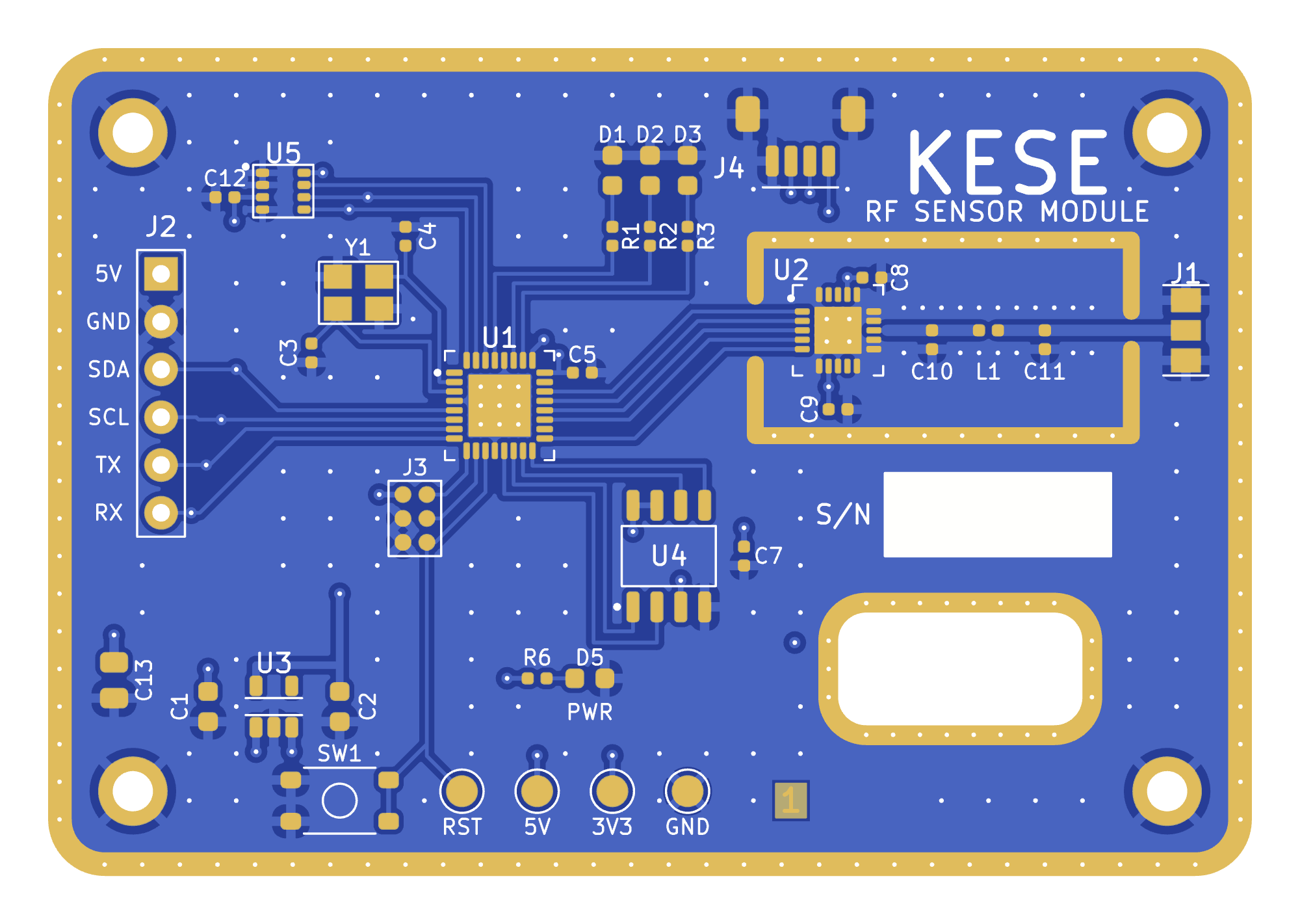
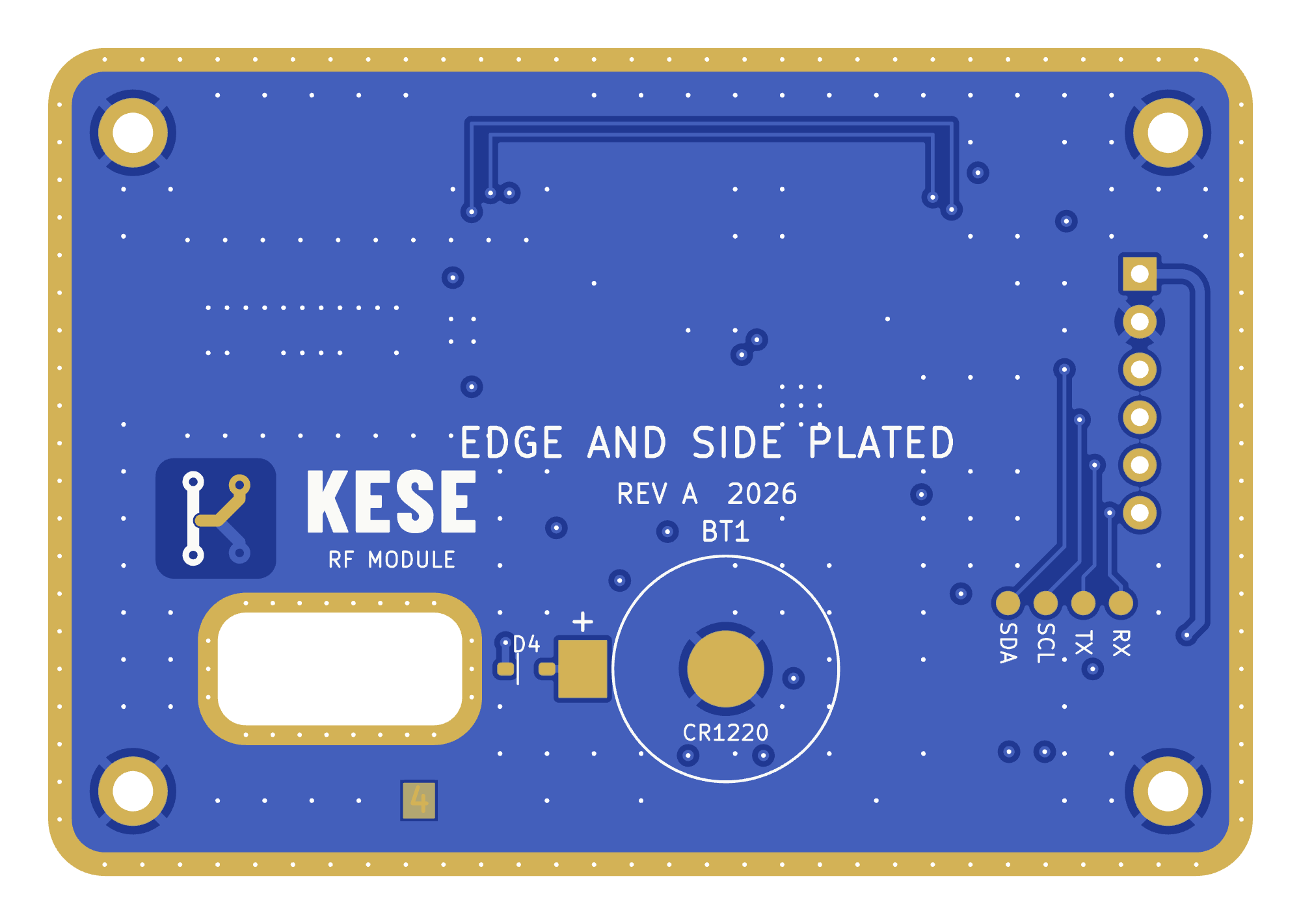
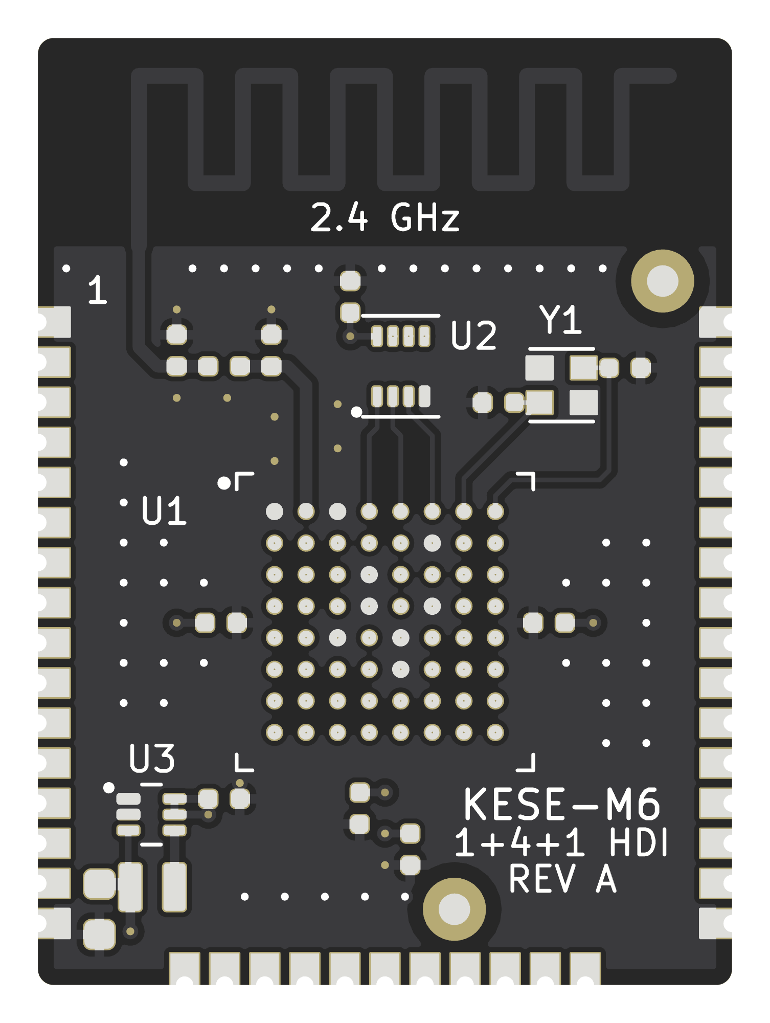
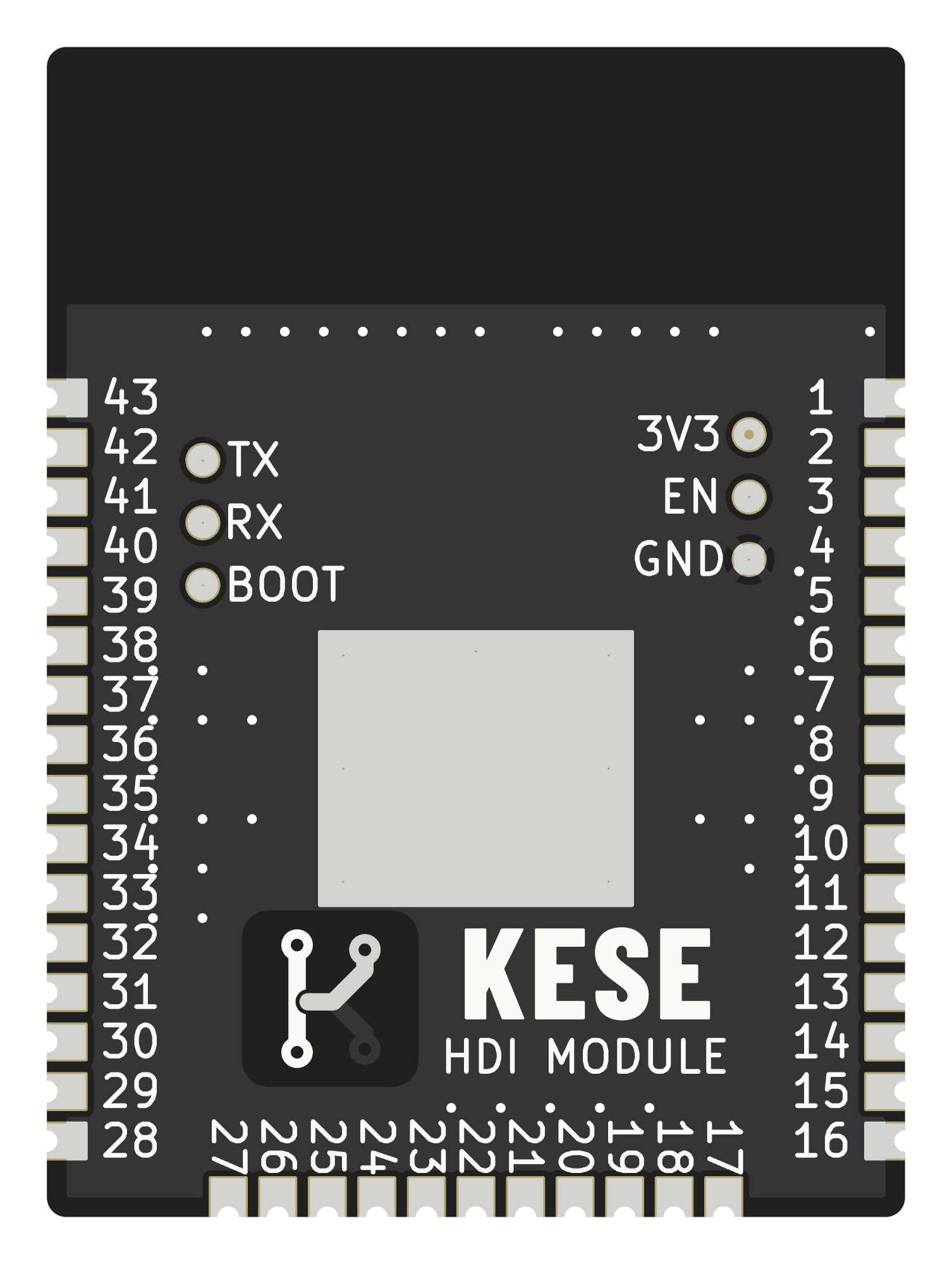
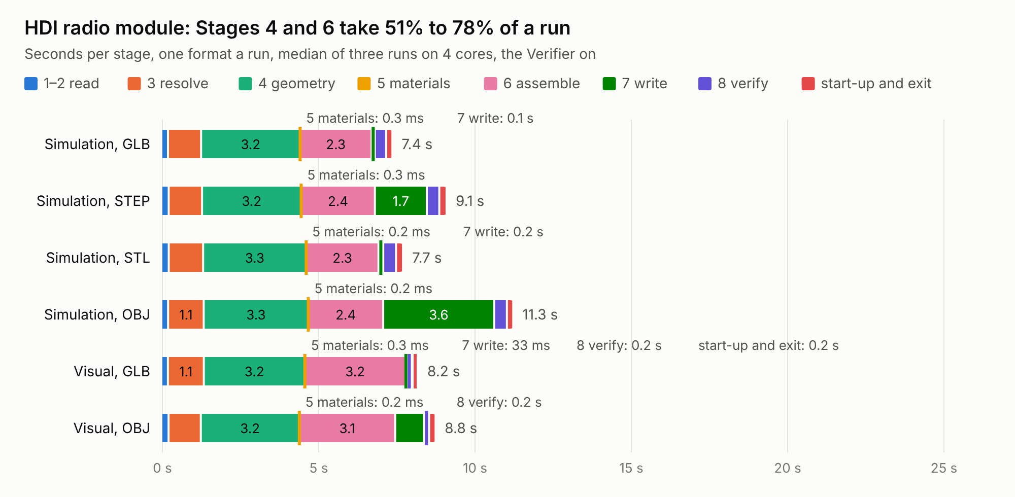
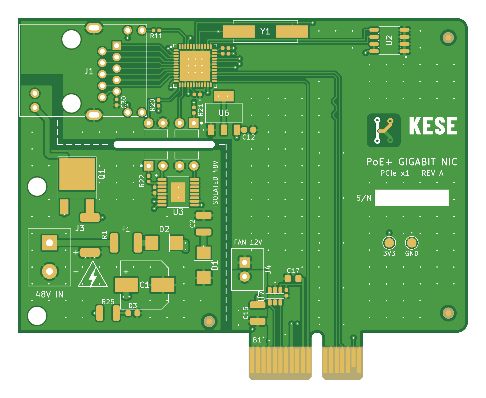
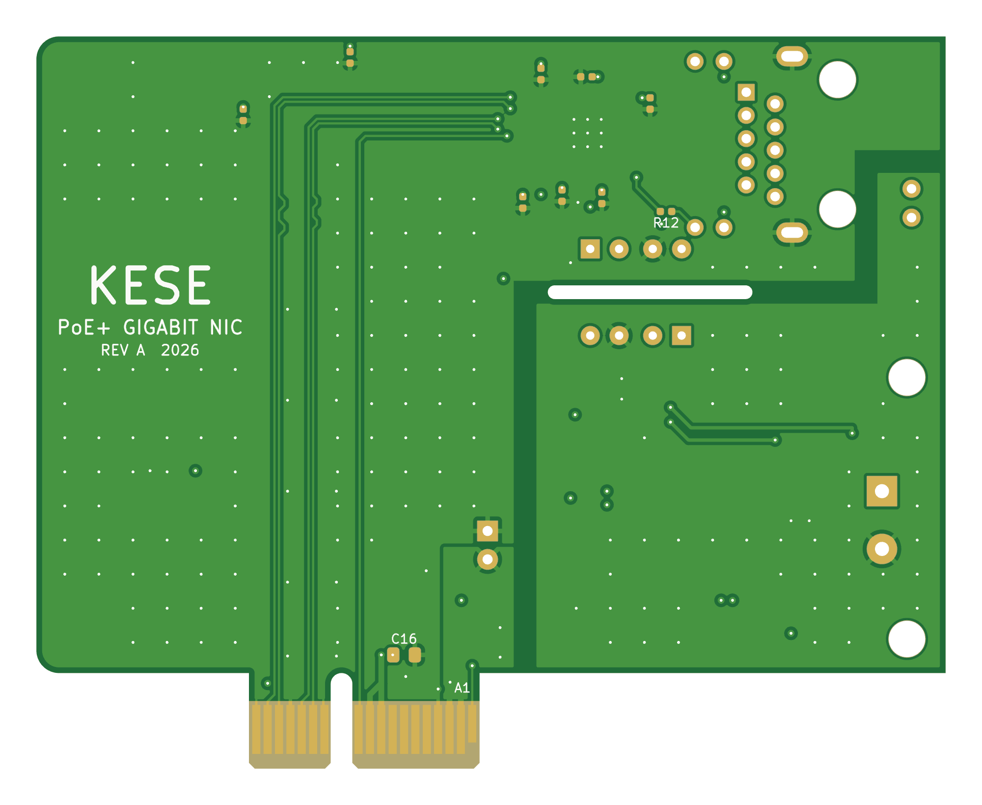
Where the time of a run goes, stage by stage, for the three example boards of Generator/Input/
(Examples). Each board was exported in every format KESE writes, one format a run:
GLB, STEP, STL and OBJ in simulation mode, and GLB and OBJ in visual mode. Each of those six runs
was made three times, with the Verifier on, and each bar is the median of the three runs for that
stage, read from the timing block of
report.txt:
python run_KESE.py Input/rf_module.kicad_pcb --mode simulation --format glb --verify
python run_KESE.py Input/rf_module.kicad_pcb --mode simulation --format step --verify
python run_KESE.py Input/rf_module.kicad_pcb --mode simulation --format stl --verify
python run_KESE.py Input/rf_module.kicad_pcb --mode simulation --format obj --verify
python run_KESE.py Input/rf_module.kicad_pcb --mode visual --format glb --verify
python run_KESE.py Input/rf_module.kicad_pcb --mode visual --format obj --verify
All 54 runs passed the Verifier. Beside each board's facts, a second table gives, for each of the
six runs, the size of the model file it writes and the most memory it used at once: the
proportional set size (PSS) of KESE's process and its workers, summed and sampled every 10 ms, the
median of three more runs. The STL size is that of the stl/ folder, one file a part, and the OBJ
size includes its .mtl. MB is a million bytes.
The runs used the default parameters on one Linux machine with 4 cores (an Intel Xeon at 2.1 GHz)
and 16 GB of RAM, so Parallel.WORKERS = 0 gave four workers
(Work Done In Parallel). On another machine the
seconds differ.
| Bar | Stages | What runs in it |
|---|---|---|
| 1–2 read | 1 read, 2 collect | The file parsed; every track, pad, zone, graphic and text as a flat shape; the stroke font unpacked and split into lines (about 0.06 s), and the glyphs the text uses parsed |
| 3 resolve | 3 | The copper joined per layer and net, clipped and drilled; barrels, edge plating, mask openings and silkscreen |
| 4 geometry | 4 | Every part as prisms, between the heights of the stack-up |
| 5 materials | 5 | A material for every part, from parameters/color.py and the stack-up's colours: 0.2 to 0.3 ms |
| 6 assemble | 6 | Closed solids in simulation mode, the visible skin in visual mode; with --verify, each solid is also checked here by the worker that built it |
| 7 write | 7 | The files, the one stage the format changes much. On the three boards GLB takes 0.11 to 0.19 s in simulation mode and 33 to 53 ms in visual mode, STL 0.15 to 0.32 s, STEP 1.7 to 2.5 s, and OBJ 3.6 to 6.9 s in simulation mode and 0.9 to 1.7 s in visual mode |
| 8 verify | 8 | The Verifier's checks of the written files (Checks, Errors And Warnings) |
| start-up and exit | none | The wall-clock time less the stages, about 0.2 s: Python starting (13 ms), KESE and the libraries it uses imported (0.12 s), the run set up and closed around the stages (14 ms), stage 9 writing report.txt and parameters.txt (1 to 3 ms), and Python freeing the run's memory as it ends (0.04 s) |
Under each chart a table gives the same numbers, in seconds unless marked ms. A stage too thin to see at this scale is marked with a line and a label.
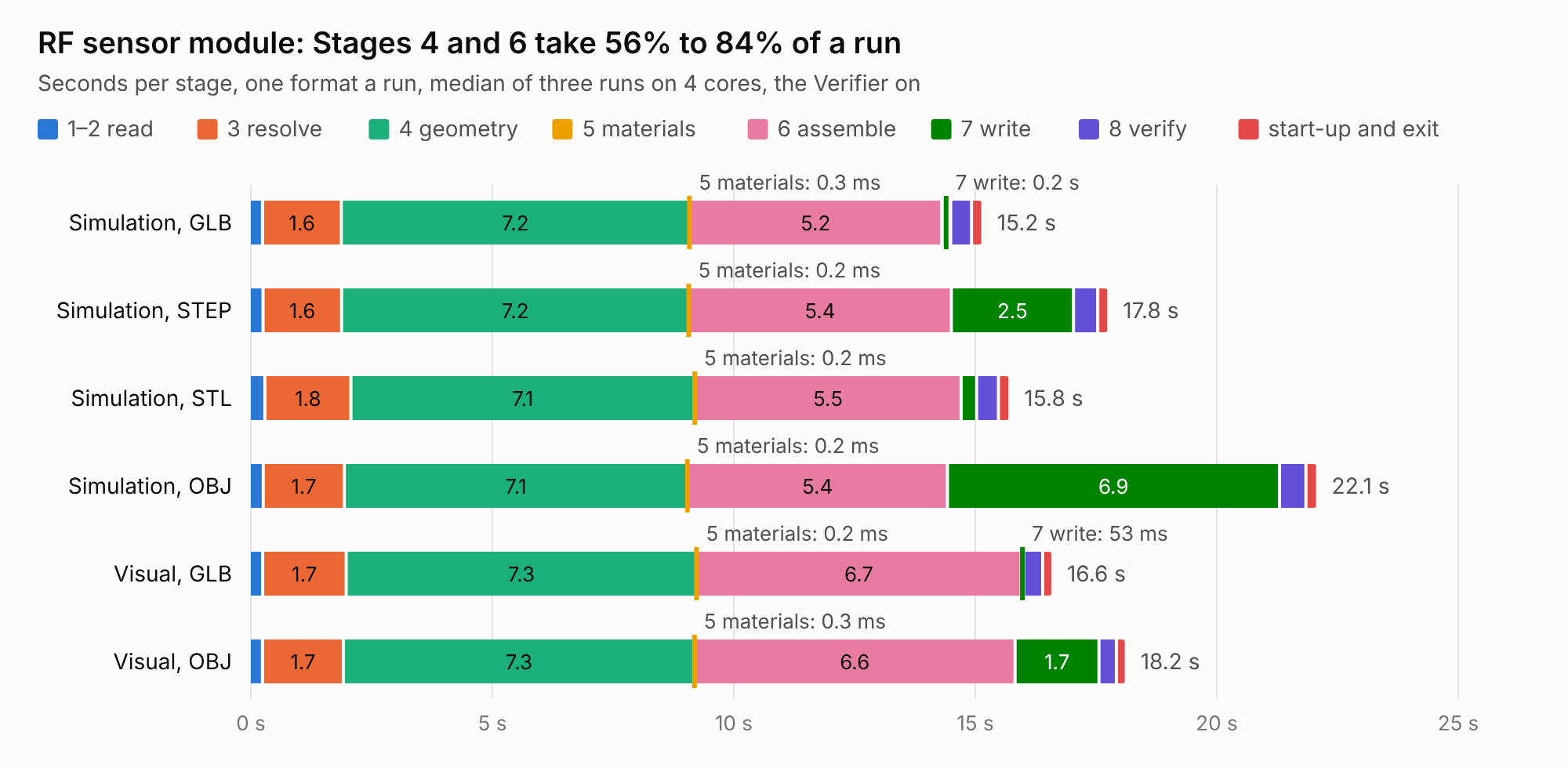
| Mode and format | 1–2 read | 3 resolve | 4 geometry | 5 materials | 6 assemble | 7 write | 8 verify | start-up and exit | Total |
|---|---|---|---|---|---|---|---|---|---|
| Simulation, GLB | 0.3 | 1.6 | 7.2 | 0.3 ms | 5.2 | 0.2 | 0.4 | 0.2 | 15.2 |
| Simulation, STEP | 0.3 | 1.6 | 7.2 | 0.2 ms | 5.4 | 2.5 | 0.5 | 0.2 | 17.8 |
| Simulation, STL | 0.3 | 1.8 | 7.1 | 0.2 ms | 5.5 | 0.3 | 0.5 | 0.2 | 15.8 |
| Simulation, OBJ | 0.3 | 1.7 | 7.1 | 0.2 ms | 5.4 | 6.9 | 0.5 | 0.2 | 22.1 |
| Visual, GLB | 0.3 | 1.7 | 7.3 | 0.2 ms | 6.7 | 53 ms | 0.4 | 0.2 | 16.6 |
| Visual, OBJ | 0.3 | 1.7 | 7.3 | 0.3 ms | 6.6 | 1.7 | 0.4 | 0.2 | 18.2 |
|
|
|||||||||||||||||||||||||||||||||||||||||
| Mode and format | 1–2 read | 3 resolve | 4 geometry | 5 materials | 6 assemble | 7 write | 8 verify | start-up and exit | Total |
|---|---|---|---|---|---|---|---|---|---|
| Simulation, GLB | 0.2 | 1.1 | 3.2 | 0.3 ms | 2.3 | 0.1 | 0.4 | 0.2 | 7.4 |
| Simulation, STEP | 0.2 | 1.1 | 3.2 | 0.3 ms | 2.4 | 1.7 | 0.4 | 0.2 | 9.1 |
| Simulation, STL | 0.2 | 1.1 | 3.3 | 0.2 ms | 2.3 | 0.2 | 0.4 | 0.2 | 7.7 |
| Simulation, OBJ | 0.2 | 1.1 | 3.3 | 0.2 ms | 2.4 | 3.6 | 0.4 | 0.2 | 11.3 |
| Visual, GLB | 0.2 | 1.1 | 3.2 | 0.3 ms | 3.2 | 33 ms | 0.2 | 0.2 | 8.2 |
| Visual, OBJ | 0.2 | 1.0 | 3.2 | 0.2 ms | 3.1 | 0.9 | 0.2 | 0.2 | 8.8 |
|
|
|||||||||||||||||||||||||||||||||||||||||
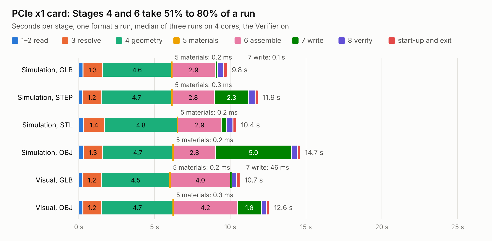
| Mode and format | 1–2 read | 3 resolve | 4 geometry | 5 materials | 6 assemble | 7 write | 8 verify | start-up and exit | Total |
|---|---|---|---|---|---|---|---|---|---|
| Simulation, GLB | 0.3 | 1.3 | 4.6 | 0.2 ms | 2.9 | 0.1 | 0.4 | 0.3 | 9.8 |
| Simulation, STEP | 0.3 | 1.2 | 4.7 | 0.3 ms | 2.8 | 2.3 | 0.4 | 0.2 | 11.9 |
| Simulation, STL | 0.4 | 1.4 | 4.8 | 0.2 ms | 2.9 | 0.3 | 0.4 | 0.2 | 10.4 |
| Simulation, OBJ | 0.3 | 1.3 | 4.7 | 0.2 ms | 2.8 | 5.0 | 0.4 | 0.2 | 14.7 |
| Visual, GLB | 0.3 | 1.2 | 4.5 | 0.2 ms | 4.0 | 46 ms | 0.4 | 0.2 | 10.7 |
| Visual, OBJ | 0.3 | 1.2 | 4.7 | 0.3 ms | 4.2 | 1.6 | 0.3 | 0.2 | 12.6 |
|
|
|||||||||||||||||||||||||||||||||||||||||
Every run writes the same block in its report.txt, after the parts and before the Verifier's
lines, so the time of any board can be read the same way. The HDI module's third simulation run
with STEP:
timing
  read              0.0631 s
  collect           0.1707 s
  resolve           1.0373 s
  geometry          3.0882 s
  materials         0.0002 s
  assemble          2.2221 s
  write             1.6603 s
  verify            0.3499 s
verify is there only when the Verifier ran. Each value is in seconds, to 0.1 ms.
| Previous | Next |
|---|---|
| Examples | Working Principle |