Contributed Flash by Muhammad Shahbaz
netfpga-10g/contrib-projects/flash
- NetFPGA-10G Specific cores
- Xilinx AXI Peripheral
- Microblaze Subsystem
This project provides a basic framework for automatic configuration of the NetFPGA-10G card's FPGA. The FPGA's two platform flash ICs are used to store configuration bitstreams. The first IC, Flash A, stores a "bootstrap" bitstream. The second IC, Flash B, can be used to store an arbitrary "user" bitstream. The configuration process is managed by the on-board CPLD. At power-up, the CPLD automatically "bootstraps" the FPGA using the bitstream in Flash A. The FPGA can then be configured quickly and easily from Flash B by the user. The figure below illustrates how the components of the project work together.

The project has three main components:
- FPGA bootstrap hardware design
- CPLD hardware design
- Software Tool (nf10_configure) for user control
The FPGA bootstrap design presents a PCIe interface to the host. It allows new bitstreams to be written into the platform flash ICs over the PCIe interface and allows the FPGA to be re-programmed with the bitstream stored in Flash B. The CPLD design contains access and configuration logic for the platform flash ICs. On power-up, the CPLD automatically reads from Flash A to configure the FPGA. Finally, the nf10_configure software tool allows the user to write bitstreams into the flash ICs and to re-configure the FPGA from Flash B.
The configuration project provides a basic framework which may be useful for incorporation into your NetFPGA-10G development projects. The configuration project currently has several important limitations that you should bear in mind:
- The FPGA always boots from Flash A on power-up;
- Booting partial bitstreams is not currently supported, although support may be added in a future release;
- Unless the user image contains the appropriate configuration logic (GPIO, axi_emc), further reconfiguration via PCIe is no longer possible after the FPGA is programmed from Flash B; the card must either be power-cycled or re-configured using a JTAG programming cable.
Follow the instructions below to setup and use the configuration project.
Prepare the NetFPGA-10G Board
Follow the instructions in the Server Mode section of the Production Test Manual to install the board in the host PC. Before you install the board in the host PC, set the DIP switch **SW3 **(mode pins) as follows: This enables slave selectmap configuration interface.
**SW3**: M0, M1, M2 is set to off, on, on
(Note that this setting differs from that described in the Production Test Manual. **SW3 **determines the source for FPGA configuration data.)
Build CPLD Bitstream
-
If you haven't already, follow the instructions in Getting Started Guide to install the Xilinx ISE Design Suite and check out a copy of the NetFPGA-10G repository from github.
-
In your local NetFPGA-10G tree, navigate to the CPLD subdirectory of the configuration project and launch Xilinx ISE:
cd netfpga-10g/contrib-projects/flash/cpld/
ise cpld.xise &
- In the design window, double-click "Implement Design" option as shown below:

The ISE flow produces a JEDEC bitstream called "cpld.jed".
- Navigate to the configuration project directory
cd netfpga-10g/contrib-projects/flash/
- Build the FPGA bootstrap design bitstream:
make
The build process can take up to an hour. The result is the FPGA bitstream stored at "bitfiles/download.bit".
-
Connect a JTAG programming cable to the NetFPGA-10G board. (The instructions in the Production Test Manual may be helpful if you're new to programming Xilinx FPGAs.)
-
Program the CPLD with cpld.jed
-
Program the FPGA with download.bit.
Programming with the JTAG cable is required only once to allow the bootstrap bitstream to be written into Flash A. The FPGA can be programmed over PCIe thereafter.
Build and install the Configuration utility
-
Ensure that the NetFPGA-10G NIC Driver is installed.
-
Ensure that 'include' folder is located under the 'contrib-projects/flash/sw/host' directory. If not, run the project makefile:
cd netfpga-10g/contrib-projects/flash
make
- Navigate to the directory in which the nf10_configure tool is stored:
cd netfpga-10g/contrib-projects/flash/sw/host/nf10_configure
- Build the software tool:
make
At the end of the build process you should find the nf10_confgure executable in the ./ directory.
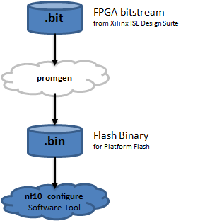
You will need to create a binary image file from each bitstream you wish to store in the platform flash ICs. FPGA bitstreams are converted into Xilinx Platform Flash-compatible binaries by the ISE PromGen tool, as shown in the flow below:
We will first create a flash binary from the FPGA bootstrap design. This must be written to Flash A by the nf10_configure tool. We will use the Production Test bitstream as a second, "user" design for Flash B. Any other user design could of course be used.
- Use the Xilinx promgen tool to convert the FPGA bootstrap design into a Flash-compatible binary image. Navigate to the configuration project root:
cd netfpga-10g/contrib-projects/flash/
- Convert the FPGA bootstrap design bitstream into a Platform Flash-compatible binary using Xilinx PromGen:
promgen -c -u 0 bitfiles/download.bit -p bin -w -data_width 8 -s 8192
The output from promgen looks like this:
Release 13.2 - Promgen O.61xd (lin64)
Copyright (c) 1995-2011 Xilinx, Inc.  All rights reserved.
0x7d6b40 (8219456) bytes loaded up from 0x0
Using user-specified prom size of 8192K
Writing file "download.bin".
Writing file "download.prm".
Writing file "download.cfi".
This creates a binary named download.bin.
- Next we'll create a second binary for Flash B using the Production Test design:
promgen -c -u 0 ../production_test/bitfiles/prod_test_no_rldram.bit -p bin -w -data_width 8 -s 8192
Write Flash Images to Flash ICs
-
Unplug the JTAG programming cable from the NetFPGA-10G and restart your PC. This causes the PCIe bus to be re-scanned.
-
Enumerate the devices on the PCIe bus:
lspci | grep Xilinx
You should see something like:
03:00.0 RAM memory: Xilinx Corporation Device 4243 (rev 02)
If you don't, the FPGA was not configured correctly with the bootstrap design. Go back to "Configure the FPGA and CPLD" and re-try those steps before proceeding.
- Load the NetFPGA-10G NIC driver (if it is not already loaded). If you're unsure whether the driver is currently loaded, do:
lsmod | grep nf10
You should see a line beginning with nf10_eth_driver. If not, follow the instructions on the Driver and User Apps page.
- Navigate to the nf10_configure directory and write the FPGA bootstrap design into Flash A:
cd netfpga-10g/contrib-projects/flash/sw/host/nf10_configure
./nf10_configure -b ../../../../bitfiles/download.bin -f a
The output from nf10_configure should look like this:
Flash image: download.bin
Manufacturer ID: **49**
Programming flash '**a**'.
[..........................................................................................
.................................................................................................
.................................................................................................
...................................]
Ensure that nf10_configure reports a flash Manufacturer ID of "49". Ensure that the CPLD and FPGA have been programmed with the correct bitstreams. Ensure also that you are writing to Flash A. The "-f" parameter allows the target Flash IC to be identified on the command line.
- Write the second, "user" design into Flash B:
./nf10_configure -b ../../../../../production_test/bitfiles/prod_test_no_rldram.bin -f b
or
./nf10_configure -b <USER_FLASH_IMAGE>.bin -f b
(Here, <USER_FLASH_IMAGE>.bin should be replaced by the path to your own design.)
-
Power-cycle your PC. When power is reapplied to the system, the NetFPGA-10G card CPLD reads the bootstrap image from Flash A and configures the FPGA with it.
-
List the devices on the PCIe bus using lspci. As before, you should see the NetFPGA card listed. If you can observe the NetFPGA-10G card's DONE and INIT LEDs (near the JTAG connector), both should be illuminated. The FPGA has successfully been configured from Flash A.
-
Load the NetFPGA-10G NIC driver, see step # 3 above.
-
In a shell, navigate to where the nf10_configure binary is stored and request the CPLD to reconfigure the FPGA from Flash B:
cd netfpga-10g/contrib-projects/flash/sw/host/nf10_configure
./nf10_configure -i
You should see:
FPGA re-initialized with flash 'b' image.
Note: issuing "nf10_configure -i" has the same effect as pressing the NetFPGA-10G board's PROG pushbutton. Regardless of which way you initiate FPGA configuration from Flash B, you should observe the DONE and INIT LEDs go out for about 1 second and then re-illuminate after the new image is written to the device.
-
Reboot your PC.
-
The FPGA should now be configured with the Production Test design. (You can verify this by following the steps outlined in the Production Test Manual if desired.)
Note: because the Production Test design used here does not include Flash configuration logic, you won't be able to reconfigure the device from Flash a second time. You will need to power-cycle the board or re-program the FPGA manually using a JTAG programming cable. Ideally, user designs for NetFPGA-10G should incorporate the Flash configuration logic provided in the configuration reference design to overcome this limitation.