Repository navigation
Chapter 2 Electrical Fundamentals
Reference for the electrical concepts underlying hardware hacking - covering voltage/current/power, digital logic levels, bus protocols (UART, SPI, I2C, JTAG), oscilloscope/logic-analyzer measurement, and signal integrity issues that affect hardware security work.
Covers: V/I/R/P relationships, digital logic levels (CMOS vs TTL, 1.8/3.3/5V), Ohm's law for shunt measurement, UART framing, SPI modes, I2C addressing, JTAG TAP state machine, oscilloscope setup, logic analyzer configuration, and practical probe tips for hardware analysis.
Provide the minimum electrical knowledge needed to safely connect to, measure, and communicate with an embedded target without damaging it or the test equipment.
- Before connecting any hardware tool (Bus Pirate, logic analyzer, oscilloscope) to an unknown target
- Reference during fault injection or power analysis setup (shunt calculation, probe loading)
- When interpreting logic analyzer captures and troubleshooting protocol issues
Part of the Hardware Hacking Guide - ULTIMATE CYBERSECURITY MASTER GUIDE
Understanding the relationships between electrical quantities is foundational for measurement, probing, and side-channel work.
| Quantity | Symbol | Unit | Relevance to Hardware Hacking |
|---|---|---|---|
| Voltage | V | Volt (V) | Supply manipulation; signal levels; logic thresholds |
| Current | I | Ampere (A) | Power analysis; shunt resistor measurement |
| Power | P | Watt (W) | P = V × I; target of power analysis attacks |
| Resistance | R | Ohm (Ω) | V = I × R (Ohm's Law); shunt selection |
| Capacitance | C | Farad (F) | Decoupling caps; affects glitch shape propagation |
| Impedance | Z | Ohm (Ω) | AC equivalent of resistance; critical for RF/probing |
Ohm's Law and Power:
V = I × R        (voltage = current × resistance)
P = V × I        (power = voltage × current)
P = I² × R       (power through a resistor)
P = V²/R         (power across a resistor)
Why it matters: In power analysis, a shunt is selected for the target's expected current, allowed supply drop, resistor dissipation, and measurement circuit. Current can be estimated from the measured drop using I = ΔV_shunt / R_shunt; signal coupling and probe loading affect what the instrument displays. There is no universal shunt value. See NewAE's measurement note and the target/instrument documentation.
A logic-level mismatch can produce invalid captures; a voltage beyond an input's absolute-maximum rating can damage hardware. Check the target and instrument specifications before connecting or driving a signal.
| Example I/O standard | Supply | VIH (minimum) | VIL (maximum) | Notes |
|---|---|---|---|---|
| 5V TTL | 5V | 2.0V | 0.8V | Check the receiving device's own specification |
| 3.3V LVTTL | 3.3V | 2.0V | 0.8V | Example standard; not every 3.3V pin uses LVTTL thresholds |
| 1.8V CMOS | 1.8V | 1.17V | 0.63V | Representative thresholds from the TI logic guide |
| 1.2V CMOS | 1.2V | 0.78V | 0.42V | Representative thresholds from the TI logic guide |
These are examples of named I/O standards, not universal voltage rules. Use the target and instrument datasheets for guaranteed VIH/VIL levels and absolute-maximum ratings. See TI's Logic Guide.
Level compatibility: A 1.8V output may not meet a receiver's required high-level threshold, while an output above the probe's absolute-maximum rating may damage the probe. Check both sides before connecting; use a level translator when required.
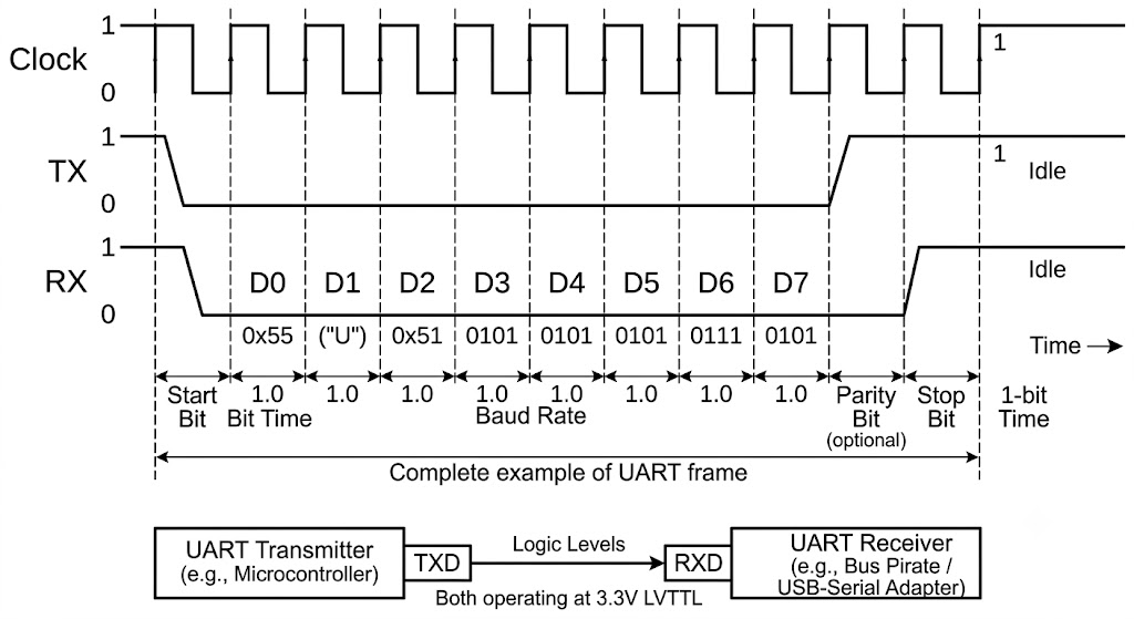
A serial interface found on some embedded boards for logs or maintenance. Whether a usable console is exposed depends on the device design and security configuration.
Signal lines: TX, RX, and a shared ground reference; a header may also expose VCC
Voltage: Common logic levels include 1.8V, 3.3V, and 5V; confirm the exact target before connecting
Framing: Start bit | 8 data bits | [Parity] | Stop bit(s)
Common baud rates: 9600, 38400, 57600, 115200, 230400, 921600
Identification:
- Look for 3–4 pin headers (VCC, GND, TX, RX) - often unpopulated in production
- Measure with oscilloscope or logic analyzer for periodic activity at boot
- Estimate candidate baud rates from captured bit timing, then verify them against a valid frame
- TX on the device = RX on your adapter (cross the connections)
- Do not connect a header's VCC unless the documented setup requires it; avoid powering the target from two sources
Possible exposure: Boot logs or a console may be available. Privilege, bootloader commands, and firmware access are device-specific; the presence of UART pins alone does not imply a shell.
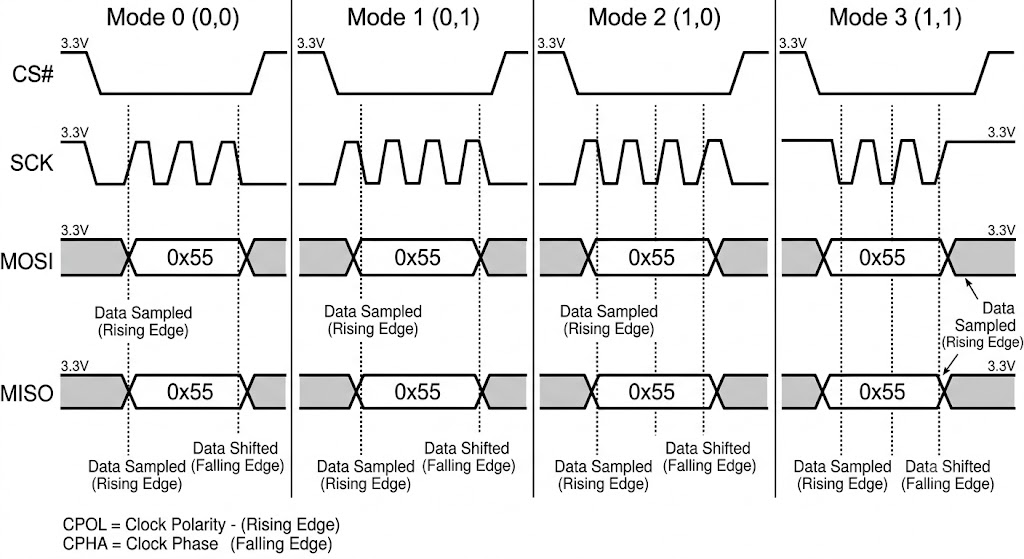
Synchronous full-duplex bus. Dominant interface for external flash memory (firmware storage), EEPROMs, DACs, ADCs.
Signal lines: SCLK, MOSI (Master Out Slave In), MISO (Master In Slave Out), CS (Chip Select, active low)
Modes: CPOL/CPHA (0,0), (0,1), (1,0), (1,1) - set clock polarity and phase
Speed: Up to tens of MHz; typically 1–25 MHz for flash
Flash chip targeting: Use only a supported flash part and adapter at the documented voltage. In-circuit reads may fail or disturb a powered board; isolate power and follow the board/programmer documentation.
# Read SPI flash with flashrom (in-circuit or removed)
flashrom -p ch341a_spi -r firmware_dump.bin

# Read with Bus Pirate
# Set SPI mode, correct speed and CPOL/CPHA for target chip
# Use flashrom or manual JEDEC commands (0x9F = Read ID, 0x03 = Read Data)

# Identify chip on board: check silkscreen, use JEDEC ID
# Common chips: W25Q series (Winbond), MX25L series (Macronix), GD25Q (GigaDevice)
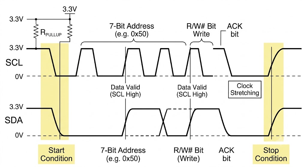
Two-wire synchronous bus. Common for configuration EEPROMs, sensors, real-time clocks, PMICs.
Signal lines: SDA (data), SCL (clock) - both open-drain with pull-up resistors
Addressing: 7-bit or 10-bit device address; a 7-bit field has 128 encodings, including reserved values
Speed: Standard (100 kHz), Fast (400 kHz), Fast-Plus (1 MHz), High-Speed (3.4 MHz)
Discovery and access: Start with the board documentation and nonintrusive voltage or logic observation. Bus scans and register reads can have device-specific side effects; writes can alter configuration or disrupt operation. Use bus tools only on an owned or explicitly authorized isolated target, with the exact controller and device documentation.
Some I²C EEPROM families use addresses in the 0x50–0x57 range, but address maps and stored data are board-specific; do not infer contents from the address alone. PMICs may expose writable power controls on some designs, but changing them can disrupt or damage a device and requires target-specific documentation and authorization.
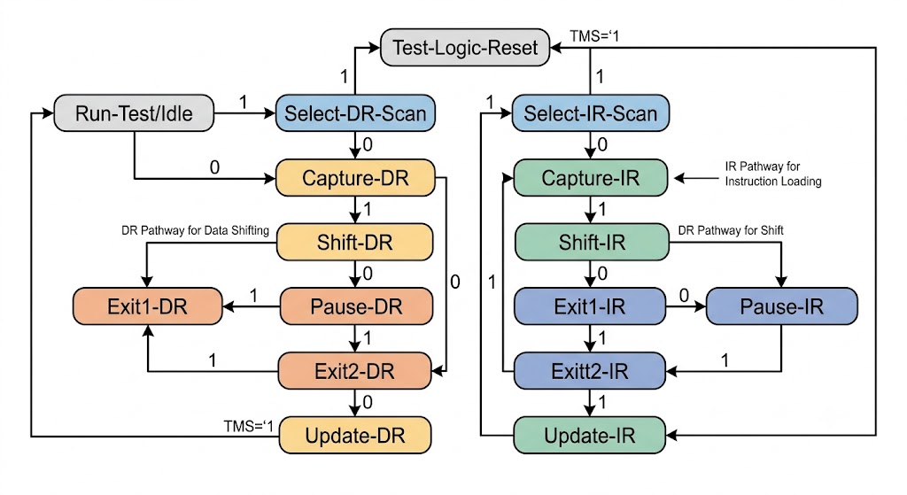
IEEE 1149.1 test interface that may also connect to a processor's debug architecture. Available operations depend on the target, debug configuration, authentication, and device lifecycle state; interface presence does not guarantee memory access or breakpoints.
Signal lines: TCK (clock), TMS (mode select), TDI (data in), TDO (data out), TRST (reset, optional)
Protocol: State machine driven by TMS; TAP (Test Access Port) controller
Identification techniques:
-
JTAGulatorhardware tool - brute-forces JTAG pinout across candidate pins - Some boards route multiple debug signals to a shared or adjacent header; verify the pinout from target documentation before connecting
-
OpenOCDwith a supported probe and matching interface, TAP, and target configuration; see the OpenOCD configuration guide
# TEMPLATE ONLY: use only with an owned/authorized target and its verified adapter/target configuration.
# Debug commands can change target state or expose protected data.
openocd -f interface/jlink.cfg -f target/stm32f4x.cfg
# In the OpenOCD session, only if permitted and supported by this exact target:
halt
dump_image authorized_lab_dump.bin 0x08000000 0x100000   # Example address/length; verify the target memory map

# Boundary scan only where supported and enabled by the exact device; verify its instruction set and pin behavior
Debug-lock enforcement and recovery behavior are device-specific. Do not assume a debug lock can be bypassed; use vendor documentation and authorized research scoped to the exact target.
ARM's two-wire debug protocol (SWDCLK and SWDIO, plus a ground reference). It is distinct from JTAG; available CoreSight features and access depend on the exact Cortex-M device, board, and debug-security configuration. See Arm's SWD documentation.
# TEMPLATE ONLY: use an owned/authorized target and its verified adapter/target configuration.
openocd -f interface/cmsis-dap.cfg -f target/nrf52.cfg
# Halt or read memory only where permitted and supported by the exact target.Choose a scope for the signal and measurement question, including the probe or differential front end. Clock rate by itself does not determine the required bandwidth or sample rate.
| Selection factor | What to check |
|---|---|
| Analog bandwidth and rise time | Compare the scope and probe response with the signal's fastest edge and frequency content of interest. |
| Sample rate | Ensure enough samples for the feature being measured. Nyquist is a theoretical lower bound for band-limited signals, not a general practical setting for edge or transient measurements. |
| Record length | Approximate capture duration is record length divided by sample rate; channel count and acquisition mode may affect available memory. |
| Vertical performance | Check input range, noise floor, effective resolution, and dynamic range. Nominal ADC bits alone do not determine whether small changes are measurable. |
| Channels and triggering | Select enough channels and trigger features for the signals and event window you need to capture. |
| Probe and input loading | Check probe bandwidth, capacitance, attenuation, differential/common-mode limits, and safe connection method. |
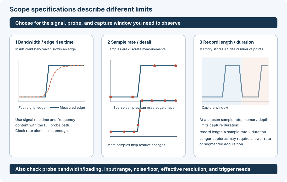
Conceptual guide: these specifications describe different limits. See Tektronix's scope performance primer and the current datasheets for the exact scope and probe. Product models and prices change; avoid assuming an unofficial bandwidth modification or option is available.
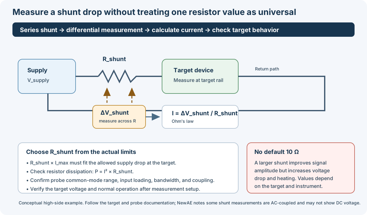
The figure shows the measurement relationship, not a fixed resistor value or tested circuit. Use the target and instrument documentation to select a safe topology and operating limits.
Place the shunt in series with the target supply and measure the voltage across it with an instrument/probe configuration suitable for the common-mode voltage and bandwidth. Estimate current using Ohm's law:
I = ΔV_shunt / R_shunt
The resistor value must be chosen for the target and measurement setup. A larger value increases signal amplitude but also increases the target's supply drop and resistor heating. Check both V_drop = I_max × R_shunt and P = I_max² × R_shunt, including the resistor's rating and the device's supply margin.
| Example R_shunt | Voltage drop at 50 mA | Interpretation |
|---|---|---|
| 1 Ω | 50 mV | Smaller drop and signal |
| 10 Ω | 500 mV | Larger drop; may disturb target operation |
| 100 Ω | 5 V | Exceeds a 3.3 V supply |
These are arithmetic examples, not recommendations for a particular target. As an illustration, if a 3.3 V target draws at most 100 mA and a 10% supply-drop budget is selected, the drop rule gives R_shunt ≤ 3.3 Ω before accounting for other rail losses. Measure the voltage at the target under its expected load.
Some instruments AC-couple shunt measurements: NewAE documents that its ChipWhisperer measure port shows voltage drop across a board shunt and does not measure DC voltage. Check the instrument's coupling, input loading, and range before interpreting a trace (ChipWhisperer power measurement notes).
| Tool | Typical role | What to verify |
|---|---|---|
| Saleae Logic 8 / Logic Pro models | Protocol decoding; some models also capture analog signals | Check the exact model datasheet. Maximum sample rate can depend on active channel count; digital sample rate, digital bandwidth, analog sample rate, and analog bandwidth are different specifications. |
| DSLogic family | Digital capture with sigrok-compatible workflows on supported models | Confirm model-specific channel count, voltage limits, sample rate, and software support. |
| Glasgow Interface Explorer | Configurable FPGA-based digital interface work | Confirm the selected applet, pin electrical limits, and achievable timing for the task. |
| Bus Pirate 5 | Protocol bridge and basic capture | Not a substitute for a dedicated logic analyzer when capture depth, timing resolution, or channel count matters. |
Use the current manufacturer documentation for the exact model and channel configuration. For example, Saleae publishes model datasheets and notes that sample rates can vary with the number of active channels (datasheets, sample-rate behavior). Avoid comparing a sample-rate number from one device with a bandwidth number from another.
Signal integrity problems can cause misleading captures, missed transitions, and unreliable measurements. The correct setup depends on the scope, probe, target, and measurement point.
- Ground reference and safety: First check whether the oscilloscope input and probe ground are earth-referenced and whether the target shares that reference. On a conventional grounded bench scope, the probe ground clip is connected to earth; attaching it to a non-ground node can short the circuit. For a floating or high-side measurement, use a correctly rated differential probe or an instrument specifically designed for that measurement. Never defeat the scope's protective earth or assume its channel grounds are isolated. For ordinary ground-referenced measurements, connect to the target's reference using the probe maker's instructions.
- Ground-lead length: Keep the probe signal and ground connections short to reduce inductance, ringing, and pickup. A long ground lead can distort fast edges; it is not a safe substitute for a proper differential measurement. See Tektronix's probing guidance.
- Probe loading: A probe changes the circuit being measured. Check the complete probe-and-scope input resistance, capacitance, bandwidth, attenuation, and voltage limits against the target and signal. A passive 10× probe may have a high DC input resistance, but its capacitance can still affect fast or high-impedance nodes; specifications vary by model. See Tektronix's probe primer.
- Decoupling and power analysis: Keep the target's decoupling capacitors in place unless the exact measurement design and target documentation call for a change. In a shunt-based power measurement, capacitors on the measured side of the shunt can divert fast current transients around the measurement resistor. Some purpose-built side-channel targets therefore specify which capacitors to omit or remove; this is a topology-specific modification, not a general rule. For example, NewAE's CW305 documentation identifies optional capacitors on a particular shunt measurement path.
- 50 Ω termination: Do not use a fixed frequency threshold. Termination depends on the interconnect, edge rise time, impedance, and source/probe/scope arrangement. A scope's 50 Ω input is a substantial load: select it only when the source, cable, probe, and test point are designed for that termination. Otherwise, use a suitable high-impedance probe/input and follow the instrument documentation. See Tektronix's probe primer.
- Onity Locks (2012) — Service Interface Case Study - Service-port trust boundaries and fleet remediation
- BusPirate.md - Implements the UART/SPI/I2C protocols described in this chapter
- HiLetgo.md - Logic analyzer for capturing the digital signals described in this chapter
- LA1010.md - Higher-speed logic analyzer for protocols requiring >24MHz capture rate
- Chapter3.md - Fault injection: applies the power/voltage concepts from this chapter to attack scenarios
- Chapter4.md - Power analysis: extends the shunt measurement and oscilloscope techniques introduced here
Next: Chapter 3 - Fault Injection Attacks →
← Chapter 1: Threat Modeling · Back to Hardware Hacking README
📄 Source: HardwareHacking/Chapter2.md | ✏️ Suggest an edit | ⬅️ Back to Hardware Hacking