Repository navigation
JTAGulator
Last reviewed: 2026-11-18
JTAGulator is an open-source tool that assists in identifying candidate on-chip debug interfaces on a target board. Current official materials describe scans for JTAG/IEEE 1149.1, ARM SWD, and UART. It automates pin-permutation checks; it does not guarantee a valid pinout, enable a locked interface, or extract firmware by itself.
The tool connects selected target test points, vias, pads, or header pins to its channels and uses target-appropriate signal levels to test supported interface patterns. A scan result is a candidate that needs independent validation. Unknown pins may have other functions, and scan activity can alter target behavior or produce false positives.
JTAGulator's VADJ configures I/O level translation. It is not a target power output: power the target through its normal, verified supply. Share ground and set VADJ to the target's documented/measured logic voltage. Hardware revisions differ; check the current documentation for supported range, pinout, and channel limits.
Help an authorized assessor narrow down candidate debug-interface pins and record evidence carefully before using a separate, compatible debugger or serial tool.
- Investigating documented or owner-approved test points and debug headers.
- Finding candidate JTAG, SWD, or UART pin assignments before confirming them with compatible equipment.
- Learning interface discovery on a known, dedicated lab board.
Designed by Joe Grand, JTAGulator is now manufactured and maintained by EXPLIoT. Current official product information lists 24 channels and an adjustable I/O range of 1.4–3.3 V; confirm the exact hardware revision and its documentation before use. Input protection does not make unknown connections risk-free. The project documentation notes that channel circuitry can affect signal levels, and a candidate scan match can be a false positive.
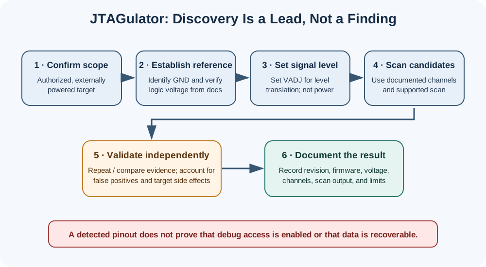
Conceptual workflow. VADJ sets signal translation levels; the target is powered separately. A scan hit is a lead to verify, not proof that debug access is enabled.
- JTAGulator project information and documentation links — design and original project information
- EXPLIoT JTAGulator product and support page — current manufacturer, revision, feature, and documentation information
- Official quick start guide — serial settings, VADJ, ground, channel connection, and cautions
- Official command reference
- Official firmware repository
Use only on a target you own or have written authorization to assess. This example discovers candidate pins; it does not attempt to bypass protections or read target contents.
- Identify the target model and revision. Review its board documentation and component datasheets for ground, test-point functions, and logic voltage.
- Power the target from its normal supply. JTAGulator does not power the target.
- Measure or verify target I/O voltage before connecting signals. Use JTAGulator's
Vcommand to set VADJ to the appropriate documented value for level translation; VADJ should not be connected to the target board. - Connect a shared ground. Confirm the target is stable and that the selected test points are appropriate. Do not probe power rails or pins whose functions and voltage are unknown.
- Connect the selected candidate signal points to sequential JTAGulator channels, starting at CH0, following the current model's connector documentation.
- Connect JTAGulator to the host and open a serial terminal at 115200 baud, 8 data bits, no parity, 1 stop bit (8N1), as specified by the official quick start.
- Follow the prompt to the JTAG functions. An IDCODE scan tests candidate signal combinations; the exact menu and command flow can vary with firmware. Use
Hfor the unit's command menu, then follow the current official guide. For firmware that uses the documented JTAG submenu,Iruns an IDCODE scan;Jcombines scan functions. - Restrict the scan to the channels actually connected. Stop if the target behaves unexpectedly, heats, resets repeatedly, or shows other signs of electrical stress.
- Treat every detected mapping as provisional. Repeat the scan and compare with board or chip documentation. False positives and nonstandard or disabled debug implementations are possible.
- Before attaching a debugger, verify the candidate pinout, voltage compatibility, reset requirements, and tool configuration. Debug access can remain locked or restricted even when pins are identified.
- Record the hardware revision, firmware version, target state, measured voltage, channels used, command, and scan output. Report only what the evidence supports.
- README.md - HardwareHacking section index and chapter guide
- BusPirate.md - USB serial protocol tool; not a JTAG debugger
- BitPirate.md - UART adapter guidance for a separately confirmed serial console
- HiLetgo.md - Logic analyzer reference for observing digital signals
- Chapter1.md - Threat modeling for physical and debug-interface access
- Chapter2.md - Electrical fundamentals, logic levels, and interface basics
📄 Source: HardwareHacking/JTAGulator.md | ✏️ Suggest an edit | ⬅️ Back to Hardware Hacking